EP0926627A1 - Méthode de commande d'un dispositif de sortie - Google Patents
Méthode de commande d'un dispositif de sortie Download PDFInfo
- Publication number
- EP0926627A1 EP0926627A1 EP98310293A EP98310293A EP0926627A1 EP 0926627 A1 EP0926627 A1 EP 0926627A1 EP 98310293 A EP98310293 A EP 98310293A EP 98310293 A EP98310293 A EP 98310293A EP 0926627 A1 EP0926627 A1 EP 0926627A1
- Authority
- EP
- European Patent Office
- Prior art keywords
- register
- value
- increment
- deviation
- indication
- Prior art date
- Legal status (The legal status is an assumption and is not a legal conclusion. Google has not performed a legal analysis and makes no representation as to the accuracy of the status listed.)
- Granted
Links
Images


Classifications
-
- G—PHYSICS
- G06—COMPUTING OR CALCULATING; COUNTING
- G06T—IMAGE DATA PROCESSING OR GENERATION, IN GENERAL
- G06T11/00—Two-dimensional [2D] image generation
- G06T11/20—Drawing from basic elements
- G06T11/23—Drawing from basic elements using straight lines or curves
Definitions
- This invention relates to methods and apparatus for controlling output devices.
- VDUs video display units
- Figure 1 illustrates a grid of pixels 1,2,etc. and a pair of lines 3,4 which are to be displayed by illuminating certain ones of the pixels.
- the shaded pixels are illuminated to display the lines.
- Line 3 presents no problems because it lies neatly along a line of pixels, passing through the centre of each one.
- line 4 lies across the lines of pixels, and when this line is displayed there is a need to digitise the continuous nature of the line by choosing the pixels that best represent the line's absolute position.
- Some pixels e.g. pixel 5 are easily chosen because the line 4 passes entirely through them.
- the line passes partially through a pair of adjacent pixels (e.g. pixels 6 and 7) there is a need to decide which of those pixels should be illuminated.
- a commonly used algorithm for digitising line segments in this context is Bresenham's algorithm (see Jack Bresenham, 1965, "Algorithm for Computer Control of a Digital Plotter", IBM Systems Journal 4(1), 25-30; reprinted in Interactive Computer Graphics, ed. H Freeman, IEEE Computer Society, 1980).
- This algorithm involves stepping pixel-by-pixel along the major axis of the line (for line 4 in figure 1 this is in the direction marked by arrow 8) and keeping track of the fractional error between the current pixel (i.e. a digitised position) and the continuous position of the line.
- the fractional error is stored as a variable known as the discriminator, which is updated at each step of the algorithm along the major axis.
- the fractional error is kept within ⁇ 0.5 pixels by testing the discriminator at each step; if the error is too large then a jump of one pixel is also made along the minor axis of the line (arrow 9 in figure 2) and the fractional error reset accordingly.
- There are equivalent algorithms for similar applications such as plotting curved lines and texture mapping and shape filling (where the stepping is generally used to find the ends of lines used to fill a shape).
- Modem graphics applications place a high demand on processing power and there is therefore a need to streamline the processing of graphics algorithms as much as possible.
- the same considerations apply to other fields where digitised data has to be output.
- a method for generating a series of digitised control values for an output device to represent a continuous series of source data comprising the steps of: storing in a single register a first digitised control value and an indication of deviation between that value and the source data; and repeatedly adding an increment to the register to generate a further digitised control value and simultaneously update the indication of deviation.
- Each further digitised control value, generated at a respective repetition, suitably represents a respective further source data point.
- the indication of deviation updated for a control value preferably represents the deviation between that control value and a respective source data point.
- the register preferably comprises a first set of adjacent bits holding the control value and a second set of adjacent bits holding the indication of deviation. Most preferably the bits of the second set of bits are the most significant bits of the register and/or act to indicate the sign of the register.
- the indication of deviation suitably represents the cumulative deviation of the control values from the source data.
- the indication of deviation may represent a discriminator.
- the increment preferably comprises a first portion for incrementing the control value and a second portion for incrementing the indication of deviation.
- the word “incrementing” should not be read to be restricted to positive incrementing, but also to include incrementing with a negative value, and the word “increment” should be read accordingly).
- the increment may suitably be selected from at least two values or may suitably be generated by a process capable of generating at least two values. In each case, there are preferably just two values. Most preferably one of these increment values is only used when the indication of deviation indicates an excessive deviation, otherwise preferably the other ("normal") increment value is used.
- the step of adding an increment may preferably be divided, at least notionally, into three stages: determining whether the previously-updated indication of deviation is excessive, selecting/generating an increment value accordingly, and adding that increment value to the register (suitably so as to accumulate the total deviation for the process so far).
- the predetermined value suitably represents a deviation of greater than half of the digitisation resolution of the output device.
- the numeric value of the indication of deviation is offset from the true deviation, suitably so as to facilitate determining whether it is excessive.
- the numeric value may be offset by half (or approximately half) of the digitisation resolution, suitably so that the numeric value of the predetermined value may be zero. This is especially preferable when the indication of deviation represents the sign of the register - then the sign of the register itself can be tested to determine whether the indication of deviation represents an excessive deviation.
- the increment value may be chosen from predetermined increment values. Alternatively it may be generated.
- One method for generating the increment value is by a masking operation.
- a mask may be generated as a function of the indication of deviation. This may, for example, be a bit shift function.
- the mask can preferably take one of two values, one having a string of zeros (or unset bits) and the other having a string of ones (or set bits).
- the increment may be generated by masking a predetermined increment value with the mask.
- a hardware implementation of means adapted to carry out the above method comprising: processing means; a data memory comprising storage registers; a program memory for storing a set of instructions for the processor to generate a series of digitised control values for an output device to represent a continuous series of source data by storing in a single register a first digitised control value and an indication of deviation between that value and the source data, and repeatedly adding an increment to the register to generate a further digitised control value and simultaneously update the indication of deviation; and output means for supplying the digitised control values to the output device.
- the output device may be a video display device/unit or a printer or a plotter.
- Each of these suitably provides a plurality of pixels or other discrete locations at which data can be displayed.
- the locations preferably lie on a grid, suitably an orthogonal grid.
- the grid is suitably in two or three dimensions.
- the control values preferably provide for controlling activation of pixels/locations of the output means.
- the source data preferably represents graphical information. In this case, where there are two available increment values, preferably one represents an increment in one direction and the other represents an increment in another direction, which is preferably normal to the said one direction.
- the source data preferably represents one or more lines (straight or curved) to be displayed by the output device.
- the method preferably implements (or provides part of an implementation of) Bresenham's algorithm.
- the step of repeatedly adding an increment to the register is preferably stored as a set of instructions for a data processing apparatus and that set of instructions preferably includes no branch instructions (e.g. jump-type instructions), most preferably no conditional branch instructions.
- the register may be of a type that can be subject to packed and non-packed instructions, i.e. instructions that treat the register as being composed of sub-units (e.g. objects) and instructions that treat the register as a whole.
- the operation of adding an increment to the register is suitably performed by a packed adding operation.
- one of the steps of determining whether the previously-updated indication of deviation is excessive and adding the increment value to the register is provided by a non-packed instruction and the other by a packed instruction.
- One or more of the instructions are preferably capable of being executed by dedicated apparatus (software or hardware) in the computer.
- the length of the register is preferably 32, 64 or 128 bits.
- FIG. 2 shows a processor in accordance with one embodiment of the present invention.
- the processor has three execution units including a conventional arithmetic unit 2 and a memory access unit 4. In addition there is a packed arithmetic unit 6.
- the processor also includes an instruction fetcher 8, an instruction register 10, a register file 12 and an instruction pointer 14, all of which operate under the control of a control unit 16 of the processor.
- the register file comprises a set of registers each having a predetermined bit capacity and each being addressable with a single address. It is not possible to address individual locations within a register. When a register is accessed, the entire contents of the register are concerned.
- the processor further includes a constant unit 18 and a select unit 20. The constant unit 18 and select unit 20 are also operated under the control of the control unit 16.
- the processor operates in conjunction with a memory 22 which holds instructions and data values for effecting operations of the processor.
- Data values and instructions are supplied to and from the memory 22 via a data bus 24.
- the data bus 24 supplies data values to and from the memory 22 via a memory data input 26.
- the data bus 24 also supplies data to the instruction fetcher 8 via a fetcher data input 28 and to the memory access unit 4 via a memory access read input 30.
- the memory is addressed via the select unit 20 on address input 32.
- the select unit 20 is controlled via a fetch signal 34 from the control unit 16 to select an address 36 from the fetcher 8 or an address 38 from the memory access unit 4.
- Read and write control lines 40,42 from the control unit 16 control read and write operations to and from the memory 22.
- the instruction fetcher 8 fetches instructions from the memory 22 under the control of the control unit 16 as follows. An address 36 from which instructions are to be read is provided to the memory 22 via the select unit 20. These instructions are provided via the data bus 24 to the fetcher data input 28. When the instruction fetcher has fetched its next instruction, or in any event has a next instruction ready, it issues a Ready signal on line 44 to the control unit 16. The instruction that is to be executed is supplied to the instruction register 10 along instruction line Inst 46 and held there during its execution. The instruction pointer 14 holds the address of the instruction being executed supplied to it from the fetcher 8 via instruction pointer line 48.
- a Get signal 47 responsive to a New Inst signal 53 from the control unit 16 causes the instruction register 10 to store the next instruction on Inst line 46 and causes the fetcher 8 to prepare the next instruction.
- the New Inst signal 53 also causes the instruction pointer 14 to store the address of the next instruction.
- a branch line 50 from the control unit 16 allows the instruction fetcher 8 to execute branches.
- the instruction register 10 provides Source 1 and Source 2 register addresses to the register file 12 as Reg1 and Reg2.
- a result register address is provided as Dest.
- Opcode is provided to the control unit 16 along line 51.
- some instructions will provide a constant operand instead of encoding one or both source registers.
- the constant is provided by the constant unit 18.
- the instruction's source values are provided on Source 1 and Source 2 buses 52,54 by the appropriate settings of the S1 Reg and S2 Reg signals at inputs E1,E2.
- the correct execution unit is enabled by providing the appropriate values for Pack Ops, Mem Ops and ALU Ops signals from the control unit 16 in accordance with the Opcode on line 51.
- the enabled unit will normally provide a result Res on a result bus 56. This is normally stored in the selected result register Dest in the register file 12. There are some exceptions to this.
- Some instructions provide a Double length result. These store the first part of the result in the normal way. In a subsequent additional stage, the second part of the result is stored in the next register in the register file 12 by asserting a Double signal 58.
- Branches 50 need to read and adjust the instruction pointer 14. These cause the S1 Reg signal not to be asserted, and so the instruction pointer 14 provides the Source 1 value on line 60.
- the Source 2 value is provided in the normal way (either from a register in the register file 12, or the constant unit 18).
- the arithmetic unit 2 executes the branch calculations and its result is stored into the fetcher 8 on the New IP input 64, rather than the register file 12, signalled by the Branch line 50 from the control unit 16. This starts the fetcher from a new address.
- Conditional branches must execute in two stages depending on the state of condition line 62.
- the first stage uses the Dest Register as another source, by asserting a Read Dest signal 45. If the condition is satisfied, then the normal branch source operands are read and a branch is executed.
- Source operands are always the natural word length. There can be one, two or three source operands.
- the execution units 2,4,6 do not hold any state between instruction execution. Thus subsequent instructions are independent.
- the arithmetic unit 2 and memory access unit 4, along with the control unit 16 can execute the following instructions of a conventional instruction set.
- a register is used to denote the contents of a register as well as a register itself as a storage location, in a manner familiar to a person skilled in the art.
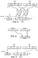
- Figure 3 shows in a block diagram the packed arithmetic unit 6. This is shown as a collection of separate units each responsible for some subset of packed arithmetic instructions. Another implementation could combine the functions in different ways.
- the units include a zip unit 74 and an obvious packed arithmetic unit 80. These are operated responsive to a route opcode unit 82 which selectively controls the arithmetic units 70 to 80. Operands for the arithmetic units 74 and 80 are supplied along the Source 1 and Source 2 buses 52,54. Results from the arithmetic units are supplied to the result bus 56.
- the op input to the route opcode unit 82 receives the Pack Ops instruction from the control unit 16 (figure 2). It will be appreciated that the operands supplied on the Source 1 and Source 2 buses are loaded into respective input buffers of the arithmetic units and the results supplied from one or two output buffers to one or two destination registers in the register file 12.
- the obvious packed arithmetic unit 80 performs operations taking the two source operands as containing several packed objects each and operating on respective pairs of objects in the two operands to produce a result also containing the same number of packed objects as each source.
- the operations supported can be addition, subtraction, comparison, multiplication, left shift, right shift etc. As explained above, by addressing a register using a single address an operand will be accessed.
- the operand comprises a plurality of objects which cannot be individually addressed.
- Figure 4 shows the symbols used in the diagrams illustrating the arithmetic units of the packed arithmetic unit 6.
- Figure 5 shows an obvious packed arithmetic unit which can perform addition, subtraction, comparison and multiplication of packed 16-bit numbers.
- the source and result bus widths are 32-bit, there are two packed objects, each 16 bits long, on each bus.
- the packing of the 16-bit numbers achieves the storage of two objects in a single register, stored as successive strings of bits in that register.
- the obvious packed arithmetic unit 80 comprises two arithmetic logical units ALU0-ALU1, each of which are controlled by opcode on line 100 which is derived form the route opcode unit 82 in figure 3.
- the 32-bit word supplied from source register 1 SRC1 contains two packed objects S1[0]-S1[1].
- the 32-bit word supplied from source register 2 SRC2 contains two packed objects S2[0]-S2[1]. These are stored in first and second input buffers 90,92.
- the first arithmetic logic unit ALU0 operates on the first packed object in each operand, S1[0] and S2[0] to generate a result R[0].
- the second arithmetic logic unit ALU1 similarly takes the second pair of objects and provides a respective result R[1]. These are stored in a result buffer 102.
- the result word thus contains two packed objects.
- An enable unit 101 determines if any of the units should be active and controls whether the output buffer asserts its output.
- the suffix "4" indicates an instruction for 32-bit objects. It is assumed that the same set of operations is provided for packed 8-bit and packed 16-bit objects, with similar names but replacing the "4" with a "1" or a "2".
- the suffix "s" in an instruction indicates that a signed operation is to be performed.
- the suffix "us” indicates that an operation is unsigned.
- Any one of these operations can alternatively be constructed from suitable combinations of the other two operations.
- the source string consists of a number of vectors, each containing the same number of equally sized objects. To name these transformations requires three numbers.
- the instruction names consist of a transform type (zip, unzip, flip), followed by the number of vectors suffixed by an "n", The size of each vector suffixed by a "v” and the object size expressed as a number of 8-bit bytes suffixed by a "p”.
- zip4n2v1pl zip denotes the instruction type
- 4n2v1pl specifies the operand format.
- a zip operation is to be executed on 4 vectors each of two one-byte objects. To do this particular operation, as each zip requires two vectors, two separate zips are done.
- Bresenham's algorithm is used in drawing line segments on, for example, a VDU.
- Figure 8 is a flow diagram illustrating the implementation.
- the implementation of figure 8 plots a line segment on a VDU having pixels arranged along orthogonal x and y axes.
- the VDU is controlled in the normal way from video memory, which in the implementation of figure 8 starts at a memory address that is held in the variable screen .
- the screen is mapped by rows and then columns into its memory space. Therefore, stepping by one memory address moves by one pixel along a row and stepping by width memory addresses moves by one pixel along a column.
- the line segment extends from position ( x1 , y1 ) to position ( x2 , y2 ).
- the major axis of the line is along the y axis, i.e. that the absolute value of x2-x1 does not exceed the absolute value of y2-y1.
- a simple substitution could be used to apply the process to line segments having the x axis as their major axis).
- the variables xDelta and yDelta are assigned to the differences between the x and y co-ordinates respectively of the end points of the line.
- the variables xStep and yStep are assigned to -1 or 1 depending on the sign of the corresponding xDelta or yDelta variable.
- the variables xAbs and yAbs are assigned to the absolute values of the corresponding xDelta or yDelta variable by multiplying that variable by the corresponding xStep or yStep variable.
- variable yStep is adjusted to equal the difference in memory addresses in the y direction between the upper and lower ends of the line. This is done by multiplying the previous value of yStep by width .
- the variable xStep already equals the difference in memory addresses in the x direction between the right and left ends of the line because the screen is mapped by rows and then columns into its memory space.
- step 504 the memory address corresponding to the first end of the line, ( x1 , y1 ), is calculated and stored in position .
- a starting value of the discriminator is calculated and stored in discriminator .
- the discriminator is held as an integer rather than a fraction. This simplifies the process, as will be shown below.
- a single variable, DAS is assigned to hold the present screen position (as a memory address) and the present value of the discriminator.
- the variable DAS is a 32-bit variable, but other sizes could be used provided they could hold the necessary information.
- the screen position is stored in a consecutive group of the least significant bits of DAS and the discriminator is stored in a consecutive group of the most significant bits of DAS .
- the computer described above is adapted to hold conveniently variables that include more than one item of data. However, in general the same effect can easily be achieved by other means - for example, if position and discriminator are 16-bit variables then DAS could be set to equal position + discriminator *2 16 .
- figure 8 adopts a convention of indicating this form of assignment by separating with a comma the two items that are being assigned.
- variables xIncrement and yIncrement are assigned to hold the values needed to increment both the present screen position and the discriminator for a step of Bresenham's algorithm in the x and y directions respectively. Since the y axis is the major axis of the line the discriminator is to be incremented by the value of xAbs for a step in the y direction, whereas the discriminator is to be incremented by negative yAbs (i.e. it is to be decremented by the value of yAbs ) for a step in the x direction.
- Step 509 sets up a loop to step along each row of the display along the major axis of the line by using counter variable pixels . This allows steps 510 to 513 to be repeated accordingly.
- Step 510 causes a pixel of the line to be drawn by making an assignment to the memory address at the address indicated by the present screen position as stored in the least significant 16 bits of DAS .
- the least significant 16 bits of DAS can be extracted by, for example, ANDing DAS with a mask - in this case with the value 2 16 -1.
- Steps 511 to 513 effect the simultaneous incrementing of both the present screen position and the discriminator.
- a check is made at 511 to find whether the discriminator is negative. Since the discriminator is stored in the most significant bits of DAS , and the most significant bit of DAS indicates its sign, this can be achieved simply by testing the sign of the entire variable DAS . If the discriminator is negative then a step along the x axis is made at 512, by adding together DAS and xIncrement . At 513 a step along the y axis is made, by adding together DAS and yIncrement . Because DAS , xIncrement and yIncrement all contain portions relevant to the screen position and the discriminator there is no need to update the screen position and the discriminator separately.
- the loop steps are repeated until the major axis of the line has been traversed.
- the instruction “zip2v4pl” is used to combine the two component parts when assigning the variables DAS , xIncrement and yIncrement .
- 4-byte packed adds (indicated by the suffix "4p” in the instructions) are used to add the variables together to increment both parts at once.
- the instruction “add4us” is used to extract the current screen position's memory address from DAS so that it can be used in the following instruction, where a value color , representing a chosen colour, is stored in the screen memory at that address.
- the instruction “jumpgez” (jump if greater than or equal to zero) is used to test the sign of DAS .
- the right shift instruction shr8s is used to produce a mask variable, mask , which replicates the sign bit of the variable DAS (i.e. the sign of the discriminator part of that variable) to make the contents of mask all ones or all zeros. This is ANDed with xIncrement to produce a variable cross . If the discriminator portion of DAS is negative then mask is all ones and cross equals xIncrement ; otherwise cross equals zero. The variable cross is then added to DAS , as is yIncrement .
- the loop has one extra step.
- the process flow is more predictable and the loop is likely to run faster on a processor that has branch prediction.
- a further speed increase might also be provided by moving the step "add4p DAS, DAS, yIncrement" back one place (or, if the same variable is used for cross and mask , back two places) so that it separates from each other the instructions that use that variable.
- the variables that hold two types of information i.e. DAS , xIncrement and yIncrement
- DAS the variables that hold two types of information
- xIncrement and yIncrement can each be held in a respective register.
- the two component items of information can then be treated as a pair of objects in each register, with the objects of each pair holding dissimilar types of information.
- one of the objects is used to control (by means of the test at step 511) the actions performed on the other (e.g. at step 512).
- the error is positive when the plotting position is inside the true location of the circle and negative when outside.
- the following code shows how the plotting of a circle can be implemented using the computer described above.
- the code plots the uppermost two octants and the lowermost two octants of the circle.
- the remaining four octants may be plotted by swapping the x and y variables in the algorithm.
- r holds the radius of the circle
- x and y hold the co-ordinates of the centre of the circle
- screen holds the lowest address of video memory
- width holds the width of the screen in memory addresses.
- the first 10 lines of the code carry out preliminary assignments to define the variables used in the body of the algorithm, setting plusx and minusx to zero, error to the value of r , y2 to (2 * r - 1), x2 to 1, screen to ( screen + x + y * width ) and y to ( r * width ).
- the variables plusx and minusx are used as offsets in the x-direction, to differentiate between the octants to the right and left of the centre-line of the circle, and the variables top and bottom as offsets in the y-direction, to differentiate between the upper and lower pairs of octants.
- a single register, errory is used to hold both the current y position and the discriminator.
- the instruction “add4ps errory, errory, x2space” increments the bits of errory that hold the discriminator, so as to update the value of the discriminator.
- the instruction “add4ps errory, errory, y2width” increments the bits of errory that hold the current y position so as to make a step in the y direction, and updates the discriminator accordingly by also incrementing the bits of errory that hold the discriminator. Since the discriminator was initially offset by r and since the sign of the discriminator determines the sign of errory , the branch instruction “jumpgez skip, errory” is very simple.
- branch instruction "jumpgez skip, errory" could be eliminated by replacing the last six lines of the code with the following:
- the present invention may include any feature or combination of features disclosed herein either implicitly or explicitly or any generalisation thereof irrespective of whether it relates to the presently claimed invention.
Landscapes
- Physics & Mathematics (AREA)
- General Physics & Mathematics (AREA)
- Engineering & Computer Science (AREA)
- Theoretical Computer Science (AREA)
- Image Generation (AREA)
- Executing Machine-Instructions (AREA)
Applications Claiming Priority (2)
| Application Number | Priority Date | Filing Date | Title |
|---|---|---|---|
| GBGB9727240.5A GB9727240D0 (en) | 1997-12-23 | 1997-12-23 | Controlling an output device |
| GB9727240 | 1997-12-23 |
Publications (2)
| Publication Number | Publication Date |
|---|---|
| EP0926627A1 true EP0926627A1 (fr) | 1999-06-30 |
| EP0926627B1 EP0926627B1 (fr) | 2003-06-11 |
Family
ID=10824164
Family Applications (1)
| Application Number | Title | Priority Date | Filing Date |
|---|---|---|---|
| EP98310293A Expired - Lifetime EP0926627B1 (fr) | 1997-12-23 | 1998-12-15 | Commande d'un dispositif de sortie |
Country Status (4)
| Country | Link |
|---|---|
| US (1) | US6903750B2 (fr) |
| EP (1) | EP0926627B1 (fr) |
| DE (1) | DE69815483D1 (fr) |
| GB (1) | GB9727240D0 (fr) |
Families Citing this family (4)
| Publication number | Priority date | Publication date | Assignee | Title |
|---|---|---|---|---|
| US6884061B2 (en) * | 2002-09-18 | 2005-04-26 | Mold-Masters Limited | Metering device for a nozzle of an injection molding apparatus |
| CN100411850C (zh) * | 2003-02-13 | 2008-08-20 | 标准模具有限公司 | 具有独立流量控制的阀浇口式注射成型系统 |
| EP1452293A1 (fr) * | 2003-02-25 | 2004-09-01 | Mold-Masters Limited | Presse à injecter avec un dispositif de régulation d'écoulement et procédé de moulage par injection |
| EP1515271A1 (fr) * | 2003-09-09 | 2005-03-16 | STMicroelectronics S.r.l. | Procédé et dispositif d'extraction d'un sous-ensemble de données à partir d'un ensemble de données |
Citations (3)
| Publication number | Priority date | Publication date | Assignee | Title |
|---|---|---|---|---|
| EP0314289A2 (fr) * | 1987-10-30 | 1989-05-03 | International Business Machines Corporation | Générateur de pixels multiples |
| EP0348631A2 (fr) * | 1988-06-27 | 1990-01-03 | Hewlett-Packard Company | Procédé de conversion de vecteur en trame |
| US5375196A (en) * | 1990-12-27 | 1994-12-20 | Calcomp Inc. | Rapid line drawing in computer graphics employing floating-point arithmetic |
Family Cites Families (3)
| Publication number | Priority date | Publication date | Assignee | Title |
|---|---|---|---|---|
| US5371839A (en) * | 1987-02-27 | 1994-12-06 | Hitachi, Ltd. | Rendering processor |
| JPH0682391B2 (ja) * | 1989-03-15 | 1994-10-19 | インターナショナル・ビジネス・マシーンズ・コーポレーション | N画素をm画素に変換する装置 |
| US5568401A (en) * | 1993-09-20 | 1996-10-22 | International Business Machines Corporation | System and method for transforming program code for efficient pixel processing |
-
1997
- 1997-12-23 GB GBGB9727240.5A patent/GB9727240D0/en not_active Ceased
-
1998
- 1998-12-15 DE DE69815483T patent/DE69815483D1/de not_active Expired - Lifetime
- 1998-12-15 EP EP98310293A patent/EP0926627B1/fr not_active Expired - Lifetime
-
2002
- 2002-04-05 US US10/117,308 patent/US6903750B2/en not_active Expired - Lifetime
Patent Citations (3)
| Publication number | Priority date | Publication date | Assignee | Title |
|---|---|---|---|---|
| EP0314289A2 (fr) * | 1987-10-30 | 1989-05-03 | International Business Machines Corporation | Générateur de pixels multiples |
| EP0348631A2 (fr) * | 1988-06-27 | 1990-01-03 | Hewlett-Packard Company | Procédé de conversion de vecteur en trame |
| US5375196A (en) * | 1990-12-27 | 1994-12-20 | Calcomp Inc. | Rapid line drawing in computer graphics employing floating-point arithmetic |
Non-Patent Citations (1)
| Title |
|---|
| ALIA G ET AL: "FAST HARDWARE GRAPHIC GENERATORS OF CURVE FAMILIES", COMPUTERS AND GRAPHICS, vol. 10, no. 1, 1986, pages 27 - 36, XP000652972 * |
Also Published As
| Publication number | Publication date |
|---|---|
| US20030071817A1 (en) | 2003-04-17 |
| DE69815483D1 (de) | 2003-07-17 |
| EP0926627B1 (fr) | 2003-06-11 |
| GB9727240D0 (en) | 1998-02-25 |
| US6903750B2 (en) | 2005-06-07 |
Similar Documents
| Publication | Publication Date | Title |
|---|---|---|
| US5859790A (en) | Replication of data | |
| US5822619A (en) | System and method for restructuring data strings | |
| US6100905A (en) | Expansion of data | |
| JP3771968B2 (ja) | コンピュータ及びコンピュータ動作方法 | |
| US5859789A (en) | Arithmetic unit | |
| US5996057A (en) | Data processing system and method of permutation with replication within a vector register file | |
| JPH02289097A (ja) | 画像表示データ処理装置 | |
| EP0743594A1 (fr) | Transposition de matrice | |
| GB1576000A (en) | Multibus processor for increasing execution speed using a pipeline effect | |
| US5604852A (en) | Method and apparatus for displaying a parametric curve on a video display | |
| US4823258A (en) | Index limited continuous operation vector processor | |
| EP0301253B1 (fr) | Génération de lignes dans un système d'affichage | |
| EP0926627B1 (fr) | Commande d'un dispositif de sortie | |
| US5020002A (en) | Method and apparatus for decomposing a quadrilateral figure for display and manipulation by a computer system | |
| US5283863A (en) | Process for effecting an array move instruction, a graphics computer system, a display system, a graphics processor and graphics display system | |
| US5717845A (en) | Method and apparatus for transferring a brush pattern to a destination bitmap | |
| US5850227A (en) | Bit map stretching using operand routing and operation selective multimedia extension unit | |
| US5265204A (en) | Method and apparatus for bit operational process | |
| US6215504B1 (en) | Line drawing using operand routing and operation selective multimedia extension unit | |
| US6538756B1 (en) | Information processing apparatus and recording medium with pattern generation programs recorded thereon | |
| US5611029A (en) | Run slice line draw engine with non-linear shading capabilities | |
| JP3547277B2 (ja) | グラフィックス処理装置 | |
| GB2226478A (en) | Converting rectilinear (x,y) information into pixel position for a raster scan display of plural horizontal resolutions | |
| GB2228597A (en) | Data processor with conditional instructions | |
| US6414692B1 (en) | Graphics processing apparatus and system |
Legal Events
| Date | Code | Title | Description |
|---|---|---|---|
| PUAI | Public reference made under article 153(3) epc to a published international application that has entered the european phase |
Free format text: ORIGINAL CODE: 0009012 |
|
| AK | Designated contracting states |
Kind code of ref document: A1 Designated state(s): DE FR GB IT |
|
| AX | Request for extension of the european patent |
Free format text: AL;LT;LV;MK;RO;SI |
|
| 17P | Request for examination filed |
Effective date: 19991202 |
|
| AKX | Designation fees paid |
Free format text: DE FR GB IT |
|
| GRAH | Despatch of communication of intention to grant a patent |
Free format text: ORIGINAL CODE: EPIDOS IGRA |
|
| RIN1 | Information on inventor provided before grant (corrected) |
Inventor name: SIDWELL, NATHAN MACKENZIE Inventor name: WATSON, VICTOR ROBERT |
|
| GRAH | Despatch of communication of intention to grant a patent |
Free format text: ORIGINAL CODE: EPIDOS IGRA |
|
| GRAA | (expected) grant |
Free format text: ORIGINAL CODE: 0009210 |
|
| AK | Designated contracting states |
Designated state(s): DE FR GB IT |
|
| PG25 | Lapsed in a contracting state [announced via postgrant information from national office to epo] |
Ref country code: IT Free format text: LAPSE BECAUSE OF FAILURE TO SUBMIT A TRANSLATION OF THE DESCRIPTION OR TO PAY THE FEE WITHIN THE PRESCRIBED TIME-LIMIT;WARNING: LAPSES OF ITALIAN PATENTS WITH EFFECTIVE DATE BEFORE 2007 MAY HAVE OCCURRED AT ANY TIME BEFORE 2007. THE CORRECT EFFECTIVE DATE MAY BE DIFFERENT FROM THE ONE RECORDED. Effective date: 20030611 |
|
| REG | Reference to a national code |
Ref country code: GB Ref legal event code: FG4D |
|
| REF | Corresponds to: |
Ref document number: 69815483 Country of ref document: DE Date of ref document: 20030717 Kind code of ref document: P |
|
| PG25 | Lapsed in a contracting state [announced via postgrant information from national office to epo] |
Ref country code: DE Free format text: LAPSE BECAUSE OF FAILURE TO SUBMIT A TRANSLATION OF THE DESCRIPTION OR TO PAY THE FEE WITHIN THE PRESCRIBED TIME-LIMIT Effective date: 20030912 |
|
| PLBE | No opposition filed within time limit |
Free format text: ORIGINAL CODE: 0009261 |
|
| STAA | Information on the status of an ep patent application or granted ep patent |
Free format text: STATUS: NO OPPOSITION FILED WITHIN TIME LIMIT |
|
| ET | Fr: translation filed | ||
| 26N | No opposition filed |
Effective date: 20040312 |
|
| PGFP | Annual fee paid to national office [announced via postgrant information from national office to epo] |
Ref country code: FR Payment date: 20051208 Year of fee payment: 8 |
|
| PGFP | Annual fee paid to national office [announced via postgrant information from national office to epo] |
Ref country code: GB Payment date: 20051214 Year of fee payment: 8 |
|
| GBPC | Gb: european patent ceased through non-payment of renewal fee |
Effective date: 20061215 |
|
| REG | Reference to a national code |
Ref country code: FR Ref legal event code: ST Effective date: 20070831 |
|
| PG25 | Lapsed in a contracting state [announced via postgrant information from national office to epo] |
Ref country code: GB Free format text: LAPSE BECAUSE OF NON-PAYMENT OF DUE FEES Effective date: 20061215 |
|
| PG25 | Lapsed in a contracting state [announced via postgrant information from national office to epo] |
Ref country code: FR Free format text: LAPSE BECAUSE OF NON-PAYMENT OF DUE FEES Effective date: 20070102 |