EP0932206A2 - High electron mobility transistor - Google Patents
High electron mobility transistor Download PDFInfo
- Publication number
- EP0932206A2 EP0932206A2 EP98124765A EP98124765A EP0932206A2 EP 0932206 A2 EP0932206 A2 EP 0932206A2 EP 98124765 A EP98124765 A EP 98124765A EP 98124765 A EP98124765 A EP 98124765A EP 0932206 A2 EP0932206 A2 EP 0932206A2
- Authority
- EP
- European Patent Office
- Prior art keywords
- layer
- thickness
- gaas
- protective layer
- cap layer
- Prior art date
- Legal status (The legal status is an assumption and is not a legal conclusion. Google has not performed a legal analysis and makes no representation as to the accuracy of the status listed.)
- Withdrawn
Links
Images


Classifications
-
- H—ELECTRICITY
- H10—SEMICONDUCTOR DEVICES; ELECTRIC SOLID-STATE DEVICES NOT OTHERWISE PROVIDED FOR
- H10D—INORGANIC ELECTRIC SEMICONDUCTOR DEVICES
- H10D30/00—Field-effect transistors [FET]
- H10D30/40—FETs having zero-dimensional [0D], one-dimensional [1D] or two-dimensional [2D] charge carrier gas channels
- H10D30/47—FETs having zero-dimensional [0D], one-dimensional [1D] or two-dimensional [2D] charge carrier gas channels having two-dimensional [2D] charge carrier gas channels, e.g. nanoribbon FETs or high electron mobility transistors [HEMT]
- H10D30/471—High electron mobility transistors [HEMT] or high hole mobility transistors [HHMT]
- H10D30/473—High electron mobility transistors [HEMT] or high hole mobility transistors [HHMT] having confinement of carriers by multiple heterojunctions, e.g. quantum well HEMT
- H10D30/4732—High electron mobility transistors [HEMT] or high hole mobility transistors [HHMT] having confinement of carriers by multiple heterojunctions, e.g. quantum well HEMT using Group III-V semiconductor material
- H10D30/4735—High electron mobility transistors [HEMT] or high hole mobility transistors [HHMT] having confinement of carriers by multiple heterojunctions, e.g. quantum well HEMT using Group III-V semiconductor material having delta-doped or planar-doped donor layers
Definitions
- the present invention generally relates to a semiconductor device, and more particularly relates to a high electron mobility transistor (HEMT) used in a millimeter wave band.
- HEMT high electron mobility transistor
- a millimeter wave band having a very wide frequency range of 30 to 300 GHz
- an active device attaining a sufficiently high gain and exhibiting excellent low-noise characteristics in the frequency range in question.
- a semiconductor layer where electrons reach a higher saturation velocity, should be used as the electron transportation layer (i.e., a channel layer). Accordingly, it was reported that if an InAlAs/InGaAs HEMT, having a channel layer made of InGaAs with a high saturation velocity, is used, then a maximum oscillation frequency fmax of more than 600 GHz, which belongs to the highest frequency band for active devices, is attained.
- this InAlAs/InGaAs HEMT also has a problem that the contact resistance of an ohmic contact layer deteriorates with the passage of time (or with the application of heat).
- a refractory metal such as tungsten (see, e.g., Jpn. J. Appl. Phys. Vol. 33 (1994), pp. 3373-3376) or molybdenum (see, e.g., Technical Report of Institute of Electronics, Information and Communication Engineers in Japan, ED93-133, CPM93-104 (1993-11), pp. 77-82) is used as a material for an ohmic electrode to prevent this deterioration with time.
- refractory metals are thermally stable and do not cause counter diffusion with indium (In).
- these refractory metals are ordinarily provided by sputtering during a fabrication process.
- Mo molybdenum
- a GaAs layer is formed between a cap layer containing In and an ohmic electrode to protect the cap layer (see, e.g., Japanese Laid-Open Publication No. 6-84958).
- a typical three-layer stack of Ti/Pt/Au may be used as a material for the electrode. Accordingly, this method easily fit in with conventional fabrication processes for GaAs MESFETs and pseudomorphic HEMTs.
- a GaAs protective layer is formed between a cap layer and an ohmic electrode. Accordingly, although the contact resistance of the electrode is low immediately after the fabrication thereof, the resistance possibly increases with time depending on the thickness of the protective layer.
- the objects of the present invention are reducing the contact resistance of an ohmic electrode and preventing the increase of the resistance with the passage of time.
- the thickness of a protective layer made of GaAs and provided between a cap layer made of a semiconductor containing In and an ohmic electrode is optimized according to the present invention.
- the semiconductor device of the present invention includes: a cap layer formed on a substrate and made of a semiconductor including In; an ohmic electrode formed over the cap layer; and a protective layer formed between the cap layer and the ohmic electrode and made of n-type GaAs.
- the protective layer prevents In atoms, contained in the cap layer, from diffusing toward the ohmic electrode and also prevents metal atoms, contained in the ohmic electrode, from diffusing toward the cap layer.
- the thickness of the protective layer is larger than 5 nm and smaller than 15 nm.
- the thickness of the n-type GaAs protective layer, formed between the cap layer made of a semiconductor including In and the ohmic electrode is larger than 5 nm and smaller than 15 nm. Accordingly, neither defects nor dislocations, which are ordinarily found in a protective layer in remarkable numbers, are caused in this protective layer. Thus, the contact resistance can be kept sufficiently low between the cap layer and the ohmic electrode and does not increase with the passage of time. As a result, a semiconductor device, exhibiting stabilized electrical characteristics for a longer period of time, can be obtained.
- the protective layer preferably includes an n-type delta doped layer.
- a well is formed in the conduction band of the n-type delta doped layer. Accordingly, the effective thickness of the energy barrier layer decreases, and therefore tunneling current is even more likely to flow than the case of providing the n-type GaAs protective layer alone. As a result, the contact resistance between the cap layer and the ohmic electrode can be further reduced.
- the substrate is preferably a semi-insulating substrate made of InP.
- a HEMT containing In can be formed with more certainty.
- the substrate is preferably a semi-insulating substrate made of GaAs.
- a HEMT can be formed at a lower cost.
- the present inventor carried out various sorts of experiments on the thickness of an n-type GaAs protective layer provided between a cap layer containing In and an ohmic electrode for protecting the cap layer. As a result, I made the following findings.
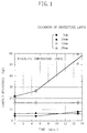
- Figure 1 illustrates respective relationships between the contact resistance and the time for various thicknesses of the GaAs protective layer formed on the InGaAs cap layer.
- the plots identified with ⁇ , ⁇ , ⁇ and ⁇ indicate cases where the thicknesses of the protective layer are 5, 10, 15 and 20 nm, respectively.
- a semi-insulating substrate made of InP and doped with iron (Fe) beforehand is used.
- an InGaAs cap layer, a GaAs protective layer and a multilayer ohmic electrode, of which the lowermost layer is made of Ti, are formed in this order on the semi-insulating substrate.
- the substrate with these layers stacked thereon is subjected to a heat treatment under the testing conditions shown in Figure 1 , i.e., annealed at 400°C for about 15 minutes within a nitrogen ambient.
- a heat treatment under the testing conditions shown in Figure 1 , i.e., annealed at 400°C for about 15 minutes within a nitrogen ambient.
- thermally stable TiAs is usually formed in the interface between GaAs and Ti (see, for example, J. Vac. Sci. Technol. A, Vol. 6, No. 3, May/June 1988).
- the properties of the interface between InGaAs and GaAs are invariable in a pseudomorphic HEMT, even if this stack is subjected to an ohmic sintering treatment at 450°C. In other words, the thermal stability of this interface has already been proven.
- the three-layer structure of InGaAs/GaAs/Ti is believed to be thermally stable.
- the contact resistance still increases in both cases where the thicknesses of the GaAs protective layer are 5 nm and 20 nm. Accordingly, if the thickness of the protective layer is larger than 5 nm and smaller than 20 nm, more preferably larger than 5 nm and smaller than 15 nm, then the thickness is optimized and the increase in contact resistance with time can be avoided. In this specification, this result will be called a "first experimental result”.
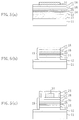
- Figures 2(a) through 2(c) schematically illustrate three types of cross-sectional structures for the three-layered semiconductor film of InGaAs/GaAs/Ti. Specifically, Figure 2(a) illustrates a case where the thickness of the GaAs layer is 5nm, which is smaller than the optimum value. Figure 2(b) illustrates a case where the thickness of the GaAs layer is at the optimum value. And Figure 2(c) illustrates a case where the thickness of the GaAs layer is about 20 nm, which is larger than the optimum value.
- the contact resistance increases in this case probably because of this phenomenon.
- the thickness of the GaAs layer is larger than the optimum value as shown in Figure 2(c) , then the contact resistance also increases. This is probably because the counter diffusion of Ti and In from the uppermost and lowermost layers, respectively, is caused through fine-line gaps formed in crystals in the GaAs layer owing to the generation of a large number of lattice defects and dislocations. Such defects and dislocations are generated because the lattice constant of InGaAs is different from that of GaAs.
- the thickness of the GaAs layer is at the optimum value in the range from more than 5 nm to less than 20 nm, then no remarkable defects or dislocations are generated in the GaAs layer as shown in Figure 2(b) .
- the interfaces between GaAs and Ti and between InGaAs and GaAs would be both kept intact and the intermediate GaAs layer would effectively function as a protective layer for the lowermost InGaAs layer.
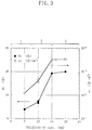
- Figure 3 illustrates respective relationships between the contact resistance and the thickness of the GaAs layer and between the specific contact resistance and the thickness of the GaAs layer in the two-layered semiconductor film of InGaAs/GaAs without taking the deterioration with time into consideration.
- the respective behaviors of the contact resistance and resistivity can be classified into the following three regions. Namely, a low-resistance region 1 with contact resistance closer to that of InGaAs; a transitional region 2 with contact resistance intermediate between those of InGaAs and GaAs; and a high-resistance region 3 with contact resistance closer to that of GaAs.
- the plots identified with ⁇ and ⁇ indicate the contact resistance Rc and the specific contact resistance rc , respectively.
- the thickness of the GaAs layer is set at 10 nm or less in the two-layered semiconductor film of InGaAs/GaAs, then low contact resistance can be obtained. In this specification, this result will be called a "second experimental result".
- the thickness of the GaAs protective layer should be in the range from more than 5 nm to less than 15 nm to keep the contact resistance low and prevent the deterioration with time.
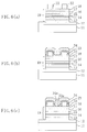
- Figure 4 illustrates a cross-sectional structure of a HEMT as a semiconductor device according to the first embodiment of the present invention.
- a buffer layer 12 made of undoped In 0.52 Al 0.48 As (thickness: 500 nm), for compensating for induced dislocations in respective semiconductor layers to be grown on an Fe-doped semi-insulating substrate 11 made of InP is formed on the principal surface thereof.
- a channel layer 13 which is made of undoped In 0.53 Ga 0.47 As (thickness: 30 nm) and where electrons move as carriers, is formed.
- a spacer layer 14 made of undoped In 0.52 Al 0.48 As (thickness: 3 nm), for separating the channel layer 13 from a Schottky layer (described below) is formed.
- an n-type delta doped layer 15 made of silicon (Si), for shortening the distance between the channel layer 13 and a gate electrode (described below) without decreasing the drain breakdown voltage and attaining a predetermined carrier density, is formed.
- a Schottky layer 16 made of undoped In 0.52 Al 0.48 As (thickness: 30 nm), for making Schottky contact with the gate electrode, is formed.
- a cap layer 17 made of n-type In 0.53 Ga 0.47 As doped with Si (thickness: 50 nm) and functioning as an ohmic contact layer, is formed. And on the cap layer 17 , a protective layer 18, made of n-type GaAs doped with Si (thickness: 7.5 nm), for protecting the cap layer 17 is formed.
- a recess is provided in the protective layer 18 and the cap layer 17 to expose the Schottky layer 16 and divide these layers 17 , 18 into two.
- a gate electrode 21 consisting of a head portion and a leg portion extending downward from the head portion, is formed in the recess.
- source/drain electrodes 22 and 23 are formed on the upper surface of the protective layer 18 .
- the protective layer 18 made of n-type GaAs to be 7.5 nm thick, is formed between the cap layer 17 made of n-type In 0.53 Ga 0.47 As and the source/drain electrodes 22 , 23 making ohmic contact with the cap layer 17 . Accordingly, a HEMT, having low contact resistance not increasing with time as described in the experimental results, can be obtained.
- Figures 5(a) through 7(c) illustrate cross-sectional structures corresponding to respective process steps for fabricating the HEMT of the first embodiment.
- the undoped In 0.52 Al 0.48 As buffer layer 12 (thickness: 500 nm)
- the undoped In 0.53 Ga 0.47 As channel layer 13 (thickness: 30 nm)
- the undoped In 0.52 Al 0.48 As spacer layer 14 (thickness: 3 nm)
- the undoped In 0.52 Al 0.48 As Schottky layer 16 thickness: 30 nm
- the n-type In 0.53 Ga 0.47 As cap layer 17 doped with Si (thickness: 50 nm)
- the n-type GaAs protective layer 18 doped with Si (thickness: 7.5 nm) are epitaxially grown in this order on the principal surface of the Fe-doped InP semi-insulating substrate 11 by an MBE technique, for example.
- the epitaxial layers are etched with a phosphate-based etchant, for example, using the first resist pattern 31 as a mask, thereby forming a mesa portion 19 out of these epitaxial layers. Then, the first resist pattern 31 is removed.
- a second resist pattern 32 having respective openings over the regions where source and drain are to be formed, is defined on the upper surface of the protective layer 18 .
- ohmic metals such as Ti, Pt and Au are evaporated in this order over the entire surface of the substrate 11 , thereby depositing a first metal film 24.
- the second resist pattern 32 is lifted off to form the source/drain electrodes 22 , 23 out of the first metal film 24 on the upper surface of the protective layer 18 .
- first EB resist film 33 made of a resist such as PMMA sensitive to electron beams (EB)
- second EB resist film 34 made of P(MMA/MAA)(i.e., poly(methylmethacrylate-co-methacrylate acid) in this order.
- the second EB resist film 34 is exposed to electron beams and developed, thereby forming a first space pattern 34a to be the head portion of the gate electrode having a size of 0.5 ⁇ m, for example, in the gate longitudinal direction.
- the first resist film 33 is irradiated with electron beams, thereby forming a second space pattern 33a to be the leg portion of the gate electrode having a size of 0.1 ⁇ m, for example, in the gate longitudinal direction.
- the cap layer 17 and the protective layer 18 are etched with a phosphate-based etchant, thereby forming the recess 17a in these layers 17 , 18 .
- gate metals such as Ti, Pt and Au are evaporated in this order over the entire surface of the substrate 11 , thereby depositing a second metal film 25 .
- the first and second EB resist films 33 , 34 are lifted off, thereby exposing the source/drain electrodes 22, 23 and forming the gate electrode 21 , consisting of the head and leg portions, out of the second metal film 25 in the recess 17a on the Schottky layer 16 as shown in Figure 7(c) .
- the n-type GaAs protective layer 18 for preventing In, contained in the cap layer 17 , from diffusing toward the ohmic electrodes, i.e., the source/drain electrodes 22, 23 , has a thickness of 7.5 nm.
- the contact resistance between the cap layer 17 and the ohmic electrodes can be reduced and kept low for a long period of time. As a result, the thermal reliability of the HEMT can be improved.
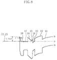
- Figure 8 illustrates the energy levels of respective semiconductor layers in the HEMT of the first embodiment.
- the energy levels of the respective layers are identified by the same reference numerals as those used in Figure 4.
- Ti contained in the source/drain electrodes 22, 23 is in Schottky contact with GaAs contained in the protective layer 18 .
- the height of the energy barrier thereof is as large as 0.75 eV.
- the thickness of the protective layer 18 is optimized at 7.5 nm and therefore tunneling current can flow through the energy barrier of the protective layer 18 . As a result, contact resistance can be kept low.
- the substrate 11 is made of InP in this embodiment.
- a semi-insulating substrate made of GaAs may also be used. Since a high-quality substrate is readily available in such a case, the fabrication cost of a HEMT can be reduced.
- a field effect transistor is exemplified as a semiconductor device of the present invention.
- the present invention is in no way limited to such an embodiment. The same effects can be attained if the present invention is applied to any other semiconductor device including a cap layer (ohmic contact layer) made of a semiconductor containing In.
- the present invention is applicable to an optical device such as a semiconductor laser device.
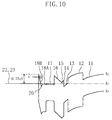
- Figure 9 illustrates a cross-sectional structure of a HEMT as a semiconductor device according to the second embodiment of the present invention.
- a buffer layer 12 made of undoped In 0.52 Al 0.48 As (thickness: 500 nm), for compensating for induced dislocations in respective semiconductor layers to be grown on an Fe-doped semiinsulating substrate 11 made of InP is formed on the principal surface thereof.
- a channel layer 13 which is made of undoped In 0.53 Ga 0.47 As (thickness: 30 nm) and where electrons move as carriers, is formed.
- a Schottky layer 16 made of undoped In 0.52 Al 0.48 As (thickness: 30 nm), for making Schottky contact with the gate electrode, is formed.
- a cap layer 17 made of n-type In 0.53 Ga 0.47 As doped with Si (thickness: 50 nm) and functioning as an ohmic contact layer, is formed.
- a first protective layer 18A made of n-type GaAs doped with Si (thickness: 3.5 nm), for protecting the cap layer 17 is formed.
- a second protective layer 18B made of n-type GaAs doped with Si (thickness: 4 nm), for protecting the cap layer 17 is formed.
- This embodiment is characterized in that a second n-type delta doped layer 20 , made of silicon, is formed between the first and second protective layers 18A, 18B for reducing the thickness of the Schottky barrier between these layers 18A , 18B .
- a recess is provided in the first and second protective layers 18A, 18B and the cap layer 17 to expose the Schottky layer 16 and divide these layers 17, 18A, 18B into two.
- the first and second protective layers 18 made of n-type GaAs to be 7.5 nm thick in total, is formed between the cap layer 17 made of n-type In 0.53 Ga 0.47 As and the source/drain electrodes 22, 23 making ohmic contact with the cap layer 17 . Accordingly, a HEMT, having low contact resistance not increasing with time as described above, can be obtained.
- the second n-type delta doped layer 20 is further provided between the first and second protective layers 18A, 18B in this embodiment.
- a well is formed in the conduction band E c of the second n-type delta doped layer 20 as shown in the energy-level diagram of Figure 10 , and the effective thickness of the energy barrier layer decreases. Accordingly, the tunneling current is even more likely to flow compared with forming the n-type GaAs protective layer alone. As a result, the contact resistance between the cap layer 17 and the source/drain electrodes 22, 23 as ohmic electrodes can be further reduced.
- Figures 11(a) through 13(c) illustrate cross-sectional structures corresponding to respective process steps for fabricating the HEMT of the second embodiment.
- the undoped In 0.52 Al 0.48 As buffer layer 12 (thickness: 500 nm)
- the undoped In 0.53 Ga 0.47 As channel layer 13 (thickness: 30 nm)
- the undoped In 0.52 Al 0.48 As spacer layer 14 (thickness: 3 nm)
- the first n-type delta doped layer 15 made of Si
- the undoped In 0.52 Al 0.48 As Schottky layer 16 thickness: 30 nm
- the n-type In 0.53 Ga 0.47 As cap layer 17 doped with Si
- the first n-type GaAs protective layer 18A doped with Si (thickness: 3.5 nm)
- the second n-type delta doped layer 20 made of Si and the second n-type GaAs protective layer 18B doped with Si (thickness
- the epitaxial layers are etched with a phosphate-based etchant, for example, using the first resist pattern 31 as a mask, thereby forming a mesa portion 19 out of these epitaxial layers. Then, the first resist pattern 31 is removed.
- a second resist pattern 32 having respective openings over the regions where source and drain are to be formed, is defined on the upper surface of the second protective layer 18B .
- ohmic metals such as Ti, Pt and Au are evaporated in this order over the entire surface of the substrate 11 , thereby depositing a first metal film 24 .
- the second resist pattern 32 is lifted off to form the source/drain electrodes 22, 23 out of the first metal film 24 on the upper surface of the second protective layer 18B.
- first EB resist film 33 made of a resist such as PMMA sensitive to electron beams (EB)
- second EB resist film 34 made of P(MMA/MAA) in this order.
- the second EB resist film 34 is exposed to electron beams and developed, thereby forming a first space pattern 34a to be the head portion of the gate electrode having a size of 0.5 ⁇ m, for example, in the gate longitudinal direction.
- the first resist film 33 is irradiated with electron beams, thereby forming a second space pattern 33a to be the leg portion of the gate electrode having a size of 0.1 ⁇ m, for example, in the gate longitudinal direction.
- the cap layer 17 , the first and second protective layers 18A, 18B and the second n-type delta doped layer 20 are etched with a phosphate-based etchant, thereby forming the recess 17a in these layers 17 , 18A, 18B and 20.
- gate metals such as Ti, Pt and Au are evaporated in this order over the entire surface of the substrate 11 , thereby depositing a second metal film 25 .
- first and second EB resist films 33, 34 are lifted off, thereby exposing the source/drain electrodes 22, 23 and forming the gate electrode 21 , consisting of the head and leg portions, out of the second metal film 25 in the recess 17a on the Schottky layer 16 as shown in Figure 13(c) .
- the contact resistance can be reduced and kept low for a long period of time. As a result, sufficiently high thermal reliability of the HEMT can be attained.
- the second n-type delta doped layer 20 is additionally formed between the first and second protective layers 18A and 18B. Accordingly, the contact resistance between the cap layer 17 and the source/drain electrodes 22, 23 as ohmic electrodes can be reduced.
- the substrate 11 is made of InP in this embodiment.
- a semi-insulating substrate made of GaAs may also be used.
- a field effect transistor is exemplified as a semiconductor device of the present invention.
- the present invention is in no way limited to such an embodiment. The same effects can be attained if the present invention is applied to any other semiconductor device including a cap layer (ohmic contact layer) made of a semiconductor containing In.
- the present invention is applicable to an optical device such as a semiconductor laser device.
Landscapes
- Junction Field-Effect Transistors (AREA)
- Electrodes Of Semiconductors (AREA)
Abstract
Description
Claims (4)
- A semiconductor device comprising:a cap layer formed on a substrate and made of a semiconductor including In;an ohmic electrode formed over the cap layer; anda protective layer formed between the cap layer and the ohmic electrode and made of n-type GaAs, the protective layer preventing In atoms, contained in the cap layer, from diffusing toward the ohmic electrode and preventing metal atoms, contained in the ohmic electrode, from diffusing toward the cap layer,
wherein the thickness of the protective layer is larger than 5 nm and smaller than 15 nm. - The device of Claim 1, wherein the protective layer comprises an n-type delta doped layer.
- The device of Claim 1, wherein the substrate is a semi-insulating substrate made of InP.
- The device of Claim 1, wherein the substrate is a semi-insulating substrate made of GaAs.
Applications Claiming Priority (2)
| Application Number | Priority Date | Filing Date | Title |
|---|---|---|---|
| JP00525398A JP3174293B2 (en) | 1998-01-14 | 1998-01-14 | Semiconductor device |
| JP525398 | 1998-01-14 |
Publications (2)
| Publication Number | Publication Date |
|---|---|
| EP0932206A2 true EP0932206A2 (en) | 1999-07-28 |
| EP0932206A3 EP0932206A3 (en) | 2000-01-26 |
Family
ID=11606065
Family Applications (1)
| Application Number | Title | Priority Date | Filing Date |
|---|---|---|---|
| EP98124765A Withdrawn EP0932206A3 (en) | 1998-01-14 | 1998-12-28 | High electron mobility transistor |
Country Status (3)
| Country | Link |
|---|---|
| US (2) | US6479896B1 (en) |
| EP (1) | EP0932206A3 (en) |
| JP (1) | JP3174293B2 (en) |
Cited By (1)
| Publication number | Priority date | Publication date | Assignee | Title |
|---|---|---|---|---|
| WO2006006134A1 (en) * | 2004-07-08 | 2006-01-19 | Koninklijke Philips Electronics N.V. | Heterostructure field effect transistor |
Families Citing this family (8)
| Publication number | Priority date | Publication date | Assignee | Title |
|---|---|---|---|---|
| JP3174293B2 (en) * | 1998-01-14 | 2001-06-11 | 松下電器産業株式会社 | Semiconductor device |
| US7921068B2 (en) * | 1998-05-01 | 2011-04-05 | Health Discovery Corporation | Data mining platform for knowledge discovery from heterogeneous data types and/or heterogeneous data sources |
| JP2004103656A (en) * | 2002-09-05 | 2004-04-02 | Sony Corp | Semiconductor device and method of manufacturing semiconductor device |
| TWI222750B (en) * | 2003-04-25 | 2004-10-21 | Univ Nat Cheng Kung | Voltage adjustable multi-stage extrinsic transconductance amplification HEMT |
| US6867078B1 (en) * | 2003-11-19 | 2005-03-15 | Freescale Semiconductor, Inc. | Method for forming a microwave field effect transistor with high operating voltage |
| JP2007103425A (en) * | 2005-09-30 | 2007-04-19 | Oki Electric Ind Co Ltd | Field effect transistor made of compound semiconductor |
| US8445941B2 (en) * | 2009-05-26 | 2013-05-21 | Bae Systems Information And Electronic Systems Integration Inc. | Asymmetrically recessed high-power and high-gain ultra-short gate HEMT device |
| US8614447B2 (en) * | 2012-01-30 | 2013-12-24 | International Business Machines Corporation | Semiconductor substrates using bandgap material between III-V channel material and insulator layer |
Family Cites Families (10)
| Publication number | Priority date | Publication date | Assignee | Title |
|---|---|---|---|---|
| JP2630446B2 (en) | 1988-10-12 | 1997-07-16 | 富士通株式会社 | Semiconductor device and manufacturing method thereof |
| JPH0812916B2 (en) | 1989-12-20 | 1996-02-07 | 日本電気株式会社 | Field effect transistor |
| JP2978972B2 (en) | 1992-03-12 | 1999-11-15 | 富士通株式会社 | Method for manufacturing semiconductor device |
| JP3108829B2 (en) | 1992-09-04 | 2000-11-13 | 富士通株式会社 | InP-based field-effect semiconductor device |
| JPH0750410A (en) * | 1993-08-06 | 1995-02-21 | Hitachi Ltd | Semiconductor crystal laminated body, method for forming the same, and semiconductor device |
| JP2581452B2 (en) | 1994-06-06 | 1997-02-12 | 日本電気株式会社 | Field effect transistor |
| JPH08107216A (en) | 1994-10-04 | 1996-04-23 | Fujitsu Ltd | Semiconductor device |
| JP3058262B2 (en) * | 1996-11-28 | 2000-07-04 | 日本電気株式会社 | Heterojunction field effect transistor |
| JP3174293B2 (en) * | 1998-01-14 | 2001-06-11 | 松下電器産業株式会社 | Semiconductor device |
| US6057566A (en) * | 1998-04-29 | 2000-05-02 | Motorola, Inc. | Semiconductor device |
-
1998
- 1998-01-14 JP JP00525398A patent/JP3174293B2/en not_active Expired - Fee Related
- 1998-12-21 US US09/217,249 patent/US6479896B1/en not_active Expired - Fee Related
- 1998-12-28 EP EP98124765A patent/EP0932206A3/en not_active Withdrawn
-
2002
- 2002-08-16 US US10/219,298 patent/US6747297B2/en not_active Expired - Fee Related
Cited By (1)
| Publication number | Priority date | Publication date | Assignee | Title |
|---|---|---|---|---|
| WO2006006134A1 (en) * | 2004-07-08 | 2006-01-19 | Koninklijke Philips Electronics N.V. | Heterostructure field effect transistor |
Also Published As
| Publication number | Publication date |
|---|---|
| JP3174293B2 (en) | 2001-06-11 |
| US20030010999A1 (en) | 2003-01-16 |
| US6747297B2 (en) | 2004-06-08 |
| US6479896B1 (en) | 2002-11-12 |
| EP0932206A3 (en) | 2000-01-26 |
| JPH11204779A (en) | 1999-07-30 |
Similar Documents
| Publication | Publication Date | Title |
|---|---|---|
| US6395588B2 (en) | Compound semiconductor device and method of manufacturing the same | |
| EP0514079B1 (en) | High electron mobility transistor and method of manufacture | |
| EP0725432B1 (en) | Refractory gate heterostructure field effect transistor and method | |
| WO1998049730A1 (en) | DESIGN AND FABRICATION OF ELECTRONIC DEVICES WITH InA1AsSb/A1Sb BARRIER | |
| US6184547B1 (en) | Field effect transistor and method of fabricating the same | |
| US5811843A (en) | Field effect transistor | |
| US6747297B2 (en) | Semiconductor device | |
| KR920003799B1 (en) | Semiconductor device | |
| EP0482726B1 (en) | Heterojunction field-effect transistor | |
| EP0080714A2 (en) | Hetero-junction semiconductor device | |
| US5180681A (en) | Method of making high current, high voltage breakdown field effect transistor | |
| US4764796A (en) | Heterojunction field effect transistor with two-dimensional electron layer | |
| JP3119248B2 (en) | Field effect transistor and method of manufacturing the same | |
| US5767539A (en) | Heterojunction field effect transistor having a InAlAs Schottky barrier layer formed upon an n-InP donor layer | |
| JPH10247727A (en) | Field-effect transistor | |
| GB2279806A (en) | Ohmic contacts for semiconductor devices | |
| US5945695A (en) | Semiconductor device with InGaP channel layer | |
| JP2005191449A (en) | Field effect transistor | |
| KR100523065B1 (en) | Method of fabricating compound semiconductor device using γ-gate electrode with stacked metal films | |
| KR910006698B1 (en) | Semiconductor device | |
| US6410946B1 (en) | Semiconductor device with source and drain electrodes in ohmic contact with a semiconductor layer | |
| JPH11111968A (en) | Manufacture of semiconductor device | |
| JP3127863B2 (en) | Semiconductor device and manufacturing method thereof | |
| JP3493205B2 (en) | Field effect transistor and method of manufacturing the same | |
| JP3233167B2 (en) | Semiconductor device |
Legal Events
| Date | Code | Title | Description |
|---|---|---|---|
| PUAI | Public reference made under article 153(3) epc to a published international application that has entered the european phase |
Free format text: ORIGINAL CODE: 0009012 |
|
| AK | Designated contracting states |
Kind code of ref document: A2 Designated state(s): DE FR GB IT |
|
| AX | Request for extension of the european patent |
Free format text: AL;LT;LV;MK;RO;SI |
|
| PUAL | Search report despatched |
Free format text: ORIGINAL CODE: 0009013 |
|
| AK | Designated contracting states |
Kind code of ref document: A3 Designated state(s): AT BE CH CY DE DK ES FI FR GB GR IE IT LI LU MC NL PT SE |
|
| AX | Request for extension of the european patent |
Free format text: AL;LT;LV;MK;RO;SI |
|
| 17P | Request for examination filed |
Effective date: 20000406 |
|
| AKX | Designation fees paid |
Free format text: DE FR GB IT |
|
| 17Q | First examination report despatched |
Effective date: 20071218 |
|
| STAA | Information on the status of an ep patent application or granted ep patent |
Free format text: STATUS: THE APPLICATION IS DEEMED TO BE WITHDRAWN |
|
| 18D | Application deemed to be withdrawn |
Effective date: 20080429 |