BACKGROUND OF THE INVENTION
Field of the Invention
The present invention relates to a distance
measurement apparatus; and, in particular, to a pulsed light
type distance measurement apparatus which emits pulsed
light toward a target to be measured and determines the
distance to the target according to the time elapsed from
the emission of light until the receiving the pulsed light
reflected by the target.
Related Background Art
There has been known a pulsed light type distance
measurement apparatus which emits pulsed light toward a
target to be measured, receives the pulsed light reflected
by the target, and determines the distance to the target
according to the time elapsed from the emission of light
until the receiving thereof.
Figs. 13A to 13H show an example of timing charts for
measurement operations during the time from the emission
to receiving in such a pulsed light type distance measurement
apparatus. The operations of the measurement apparatus are
controlled according to the reference clock shown in Fig.
13A. At the point in time where the measurement start signal
S50 shown in Fig. 13B, which also acts as an emission trigger
signal, is switched from Low level to High level, an emission
pulse L50 is emitted toward a target as shown in Fig. 13C.
The light reflected by the target is received and is
converted into an electric signal by a photoelectric
converter, so as to yield a light-receiving signal S52 shown
in Fig. 13D. Then generated is a measurement stop signal
S53 which switches from Low level to High level at the peak
point of the light-receiving signal S52. The time
difference T between the rising of measurement start signal
S50 and the rising of measurement stop signal S53 corresponds
to the time difference between the emission and receiving.
For measuring the time T with an accuracy higher than
the cycle of the reference clock, there has been known a
technique in which a fractional time Ta (see Fig. 13F)
corresponding to the time elapsed from the rising of
measurement start signal S50 until the rising of the second
reference clock therefrom, for example, and a fractional
time Tb (see Fig. 13G) corresponding to the time elapsed
from the rising of measurement stop signal S53 until the
rising of the second reference clock therefrom, for example,
are determined by a time/voltage converter, and the
reference clock number N (see Fig. 13H) from the end of Ta
to the end of Tb is counted.
SUMMARY OF THE INVENTION
In such an apparatus, however, there is a possibility
that, in the case of short distance measurement in which
the time T from the emission to receiving is short, the rising
time of Ta and the falling time of Tb may be so close to
each other that an overlap occurs, whereby their waveforms
may be disturbed upon simultaneous switching as shown in
Figs. 14A and 14B. If the waveforms of signal edges are
disturbed upon simultaneous switching of the start-side and
stop-side fractional time signals, then their edge
positions, i.e., their respective pulse widths Ta and Tb,
cannot correctly be measured. As a consequence, errors in
measurement of start-side and stop-side fractional times
will increase, so that the time from the emission of pulsed
light to the receiving thereof cannot correctly be measured,
whereby the accuracy in measurement of the distance to the
target will deteriorate.
Therefore, it is an object of the present invention
to provide a distance measurement apparatus which
eliminates errors in measurement of fractional times,
thereby improving the accuracy in short distance
measurement.
In order to achieve the above-mentioned object, the
distance measurement apparatus in accordance with the
present invention comprises the following constituents a)
to j):
In accordance with the present invention, since the
delay circuit of c) is provided, as the emission trigger
signal is delayed with respect to the measurement start
signal and/or the measurement stop signal is delayed with
respect to the receiving of reflected pulsed light, the
measurement start signal and the measurement stop signal
can sufficiently be separated from each other in terms of
time. As a result, the start-side fractional time signal
pulse and the stop-side fractional time signal pulse are
shifted from each other in terms of time. These pulses would
not overlap each other, when the delay time itself in the
case of delaying one of the emission trigger signal and
measurement stop signal or the sum of delay times in the
case of delaying both of the signals is made greater than
the maximum value of the start-side fractional time signal
pulse width. As a consequence, the error in measurement of
fractional times caused by simultaneous switching would be
eliminated, whereby the accuracy in short distance
measurement would improve.
In particular, in the case of delaying both of the
signals, the delay time setting of each signal can be set
to a short period of time which is adjustable with high
accuracy, whereby, even when the sum of delay times is long,
the total delay time can be set with higher accuracy than
in the case of delaying only one of the signals.
Further, in accordance with the present invention, the
respective pulse widths of start-side fractional time
signal pulse and stop-side fractional time signal pulse are
measured by fractional time measurement sections separated
from each other. Therefore, even when the start-side
fractional time signal pulse and the stop-side fractional
time signal pulse are close to each other, the respective
pulse widths of these fractional time signal pulses can be
measured with high accuracy, and the total measurement time
can be shortened. Usually, in a distance measurement
apparatus, several thousand measured values are averaged
for improving the accuracy in measurement, and the result
thereof is outputted or displayed. For preventing errors
in measurement from occurring upon simultaneous switching,
it is preferred that the start-side fractional time signal
pulse and stop-side fractional time signal pulse be
separated from each other as much as possible in terms of
time. This would elongate the total measurement time,
however. The present invention has fractional time
measurement sections independent of each other, so that both
signals can be made as close to each other as possible in
terms of time while keeping them from overlapping each other,
thereby being capable of preventing errors in measurement
from occurring upon simultaneous switching and allowing the
total measurement time to decrease.
The distance measurement apparatus in accordance with
another aspect of the present invention comprises the
following constituents 1) to 11):
In accordance with this aspect of the present
invention, since the measurement stop signal is delayed by
the delay circuit of 4), the measurement start signal and
the measurement stop signal can sufficiently be separated
from each other in terms of time. As a result, the start-side
fractional time signal pulse and the stop-side fractional
time signal pulse are shifted from each other in terms of
time. When the delay time is made greater than the maximum
value of the start-side fractional time signal pulse width,
then these pulses would not overlap each other in terms of
time. As a consequence, the error in measurement of
fractional times caused by simultaneous switching would be
eliminated, whereby the accuracy in short distance
measurement would improve.
Also, since the actual emission of the pulsed light
is employed as the measurement start signal, the correct
time from the emission to receiving can be determined even
when there is a temporal shift between the emission trigger
signal and the pulsed light emission. Therefore,
measurement with higher accuracy is possible.
Further, the respective pulse widths of start-side
fractional time signal pulse and stop-side fractional time
signal pulse are measured by fractional time measurement
sections separated from each other in accordance with this
aspect of the present invention as well. Therefore, even
when the start-side fractional time signal pulse and the
stop-side fractional time signal pulse are close to each
other, the respective pulse widths of these fractional time
signal pulses can be measured with high accuracy, and the
total measurement time can be shortened.
The present invention will be more fully understood
from the detailed description given hereinbelow and the
accompanying drawings, which are given by way of
illustration only and are not to be considered as limiting
the present invention.
Further scope of applicability of the present
invention will become apparent from the detailed
description given hereinafter. However, it should be
understood that the detailed description and specific
examples, while indicating preferred embodiments of the
invention, are given by way of illustration only, since
various changes and modifications within the spirit and
scope of the invention will be apparent to those skilled
in the art from this detailed description.
BRIEF DESCRIPTION OF THE DRAWINGS
Fig. 1 is a block diagram showing a first embodiment
of the distance measurement apparatus in accordance with
the present invention;
Fig. 2 is a block diagram showing the time measurement
section of the apparatus shown in Fig. 1;
Fig. 3 is a block diagram showing a time/voltage
converter of the time measurement section shown in Fig. 2;
Fig. 4 is a block diagram showing the delay circuit
portion of the apparatus shown in Fig. 1;
Figs. 5A to 5D are timing charts for explaining
operations of the delay circuit shown in Fig. 4;
Figs. 6A to 6J are timing charts for explaining
measurement operations of the apparatus shown in Fig. 1;
Fig. 7 is a block diagram showing a second embodiment
of the distance measurement apparatus in accordance with
the present invention;
Figs. 8A to 8J are timing charts for explaining
measurement operations of the apparatus shown in Fig. 7;
Fig. 9 is a block diagram showing a third embodiment
of the distance measurement apparatus in accordance with
the present invention;
Figs. 10A to 10K are timing charts for explaining
measurement operations of the apparatus shown in Fig. 9;
Fig. 11 is a block diagram showing a fourth embodiment
of the distance measurement apparatus in accordance with
the present invention;
Figs. 12A to 12M are timing charts for explaining
measurement operations of the apparatus shown in Fig. 11;
Figs. 13A to 13H are timing charts for explaining
measurement operations of a conventional distance
measurement apparatus; and
Figs. 14A and 14B are views for explaining
simultaneous switching in the conventional distance
measurement apparatus.
DESCRIPTION OF THE PREFERRED EMBODIMENTS
In the following, some of preferred embodiments of the
present invention will be explained with reference to the
accompanying drawings. To facilitate the comprehension of
the explanation, the same reference numerals denote the same
parts, where possible, throughout the drawings, and a
repeated explanation will be omitted.
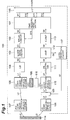
Fig. 1 is a block diagram of a distance measurement
apparatus 100 which is a first embodiment in accordance with
the present invention. A microprocessor 115 outputs a
measurement start command signal S1 for starting
measurement operations to a time measurement section 101;
determines a distance to a target 114 according to
measurement data S10, S11, and S12 fed therein from the time
measurement section 101; and outputs thus determined
distance to an OUT terminal.
According to the measurement start command signal S1
from the microprocessor 115, the time measurement section
101 outputs a measurement start signal S2 to a delay circuit
102 and measures a measurement time T. The measurement time
T is a period of time elapsed from when the measurement start
signal S2 becomes High level until a measurement stop signal
S9 outputted from a comparator section 113 which will be
explained later attains High level. The signal S13 depicted
herein is a clock signal for controlling the emission of
pulsed light, which is generated by the time measurement
section 101 and is used for adding a predetermined delay
time Td to the measurement start signal S2.
The delay circuit 102 is used for delaying the
measurement start signal S2 by the delay time Td to generate
a signal S3, and outputs this signal S3 to a laser drive
circuit 103.
The laser drive circuit 103 outputs, in
synchronization with the signal S3, a laser drive signal
S4 for driving a laser diode 104 to the latter.
A first light-transmitting optical system 105
connected to the laser diode 104 incorporates therein a half
mirror for splitting the incident pulsed light L1 into pulsed
light L2 and pulsed light L3, and the like. The pulsed light
L2 is directed to an outer optical path for emitting light
out of the apparatus, whereas the pulsed light L3 is directed
to an inner optical path which forms an optical path only
within the apparatus.
Disposed on the exit side of the first light-transmitting
optical system 105 is a movable optical path
switching sector 106 which blocks one of the optical paths
of the pulsed light L2 and pulsed light L3, thereby selecting
the inner or outer optical path. Fig. 1 shows the state where
the optical path switching sector 106 blocks the pulsed light
L3, thus selecting the outer optical path.
Disposed on the inner optical path are an inner optical
attenuator 116 for adjusting the quantity of light to a
predetermined level, and a second light-receiving optical
system 110 which will be explained later. Disposed on the
outer optical path, on the other hand, is a second
light-transmitting optical system 107 which emits pulsed
light L4 to the target 114.
A first light-receiving optical system 108 receives
pulsed light L5 reflected by the target 114 and is optically
connected, by way of an outer optical attenuator 109 for
adjusting the quantity of light, to the second light-receiving
optical system 110. Among them, the outer optical
attenuator 109 has a density or transmissivity which can
continuously be changed by an output signal of a level
detection circuit 117 which will be explained later.
The second light-receiving optical system includes
therein a half mirror and the like, and guides the pulsed
light L3 or L7 introduced from the outer or inner optical
path to a photoelectric converter section 111 as pulsed light
L8.
The photoelectric converter section 111 comprises an
optical band-pass filter, a light-receiving device, a
current/voltage converter device, and the like, and
generates an electric light-receiving signal S5 in response
to the receiving of the pulsed light L8. The output of the
photoelectric converter section 111 is connected to the
input side of an amplifier section 112, which outputs the
signal S8 in which the input signal S5 has been amplified
and a signal S6 which is proportional to the magnitude of
the input signal S5. A comparator section 113 is connected
to the amplifier section 112 such as to receive the signal
S8, whereas the level detection circuit 117 is connected
to the amplifier section 112 such as to receive the signal
S6.
The comparator section 113 includes a peak detection
circuit, outputs a stop signal S9 which is switched to High
level in response to a peak point of the signal S8, and is
connected to the time measurement section 101.
Fig. 2 is a detailed block diagram of the time
measurement section 101 in this embodiment.
The time measurement section 101 is provided with a
laser diode lighting clock oscillator (hereinafter referred
to as LD lighting clock) 204 for generating the clock signal
S13. The clock signal S13 of the LD lighting clock 204 is
split into two, one of which becomes an output of the time
measurement section 101 as it is, whereas the other is
connected to an input end of a divider circuit 203. The
output S2 of the divider circuit 203 is also split into two,
one of which becomes an output of the time measurement
section 101, whereas the other is connected to an input end
of a start-side fractional time signal generator 212.
The time measurement section 101 further comprises a
reference clock oscillator 211 for generating a reference
clock signal S30 for the whole system, and the output end
of the reference clock oscillator 211 is connected to one
input end each of the start-side fractional time signal
generator 212, a stop-side fractional time signal generator
217, and an AND circuit 215. Fed into an input end of the
stop-side fractional time signal generator 217 is the
measurement stop signal S9.
Among them, the start-side or stop-side fractional
time signal generator 212, 217 is turned on when the
measurement start signal S2 or measurement stop signal S9
becomes High level, and then generates a signal S31, S32
whose pulse width is a time Ta or Tb elapsed until the
occurrence of the reference clock signal S30 issued after
the lapse of a predetermined time.
Each of the outputs of the start-side and stop-side
fractional time signal generators 212 and 217 is split into
two, one pair of these signals are connected to S and R
terminals of an SR flip-flop 214, respectively. Outputted
from the Q terminal of the SR flip-flop 214 is a gate signal
S33 which attains H level during the period from the falling
edge of the pulse signal S31 to the falling edge of the pulse
signal S32. This Q terminal is connected to an input end
of the AND circuit 215 which is different from the input
end for the reference clock signal S31. The output end of
the AND circuit 215 is connected to a counter 216, whose
output signal is the signal S11.
The other pair of split outputs of the start-side and
stop-side fractional time signal generators 212 and 217 are
connected to time/ voltage converters 213 and 218,
respectively. These time/ voltage converters 213 and 218
convert the respective pulse widths of the start-side
fractional time signal S31 and stop-side fractional time
signal S32 into analog voltages, and thus obtained analog
voltages into the digital data signals S10 and S12, which
are then outputted to the microprocessor 115. Fig. 3 shows
their specific block diagram. Though the time/voltage
converter 213 is depicted here, the time/voltage converter
218 has a similar configuration.
The time/voltage converter 213 is constituted by a
constant-current circuit 250, an inverter 251, npn
transistors 252, 256, a diode 253, an amplifier 254, an A/D
converter 255, and a capacitor 257.
The signal input end (for receiving the signal S31)
of the time/voltage converter 213 is connected to the input
end of the inverter 251, whereas the output end of the
inverter 251 is connected to the base terminal of the
transistor 252. The base terminal of the transistor 256 is
connected to a reset terminal. Both of the transistors 252,
256 are grounded at their emitter terminals.
The collector terminal of the transistor 252 is
connected between the current-output terminal of the
constant-current circuit 250 and the anode end of the diode
253. The collector terminal of the transistor 256 is
connected to one end of the capacitor 257 having the other
end being grounded, and then is split into two which are
connected to the cathode end of the diode 253 and the input
end of the amplifier 254, respectively. The output end of
the amplifier 254 is connected to the input end of the A/D
converter 255.
Fig. 4 is a view showing an example of the delay circuit
102 used in the distance measurement apparatus 100 of this
embodiment. Connected to two input terminals of this delay
circuit 102 are the output end of the divider circuit 203
(measurement start signal S2) and the output end of the LD
lighting clock 204 (clock signal S13) within the time
measurement section 101, respectively. The delay circuit
102 is constituted by two D flip- flops 201 and 202 connected
in series, such that the Q1 terminal of the input-side D
flip-flop 202 and the D terminal of the output-side D
flip-flop 201 are connected together, whereby the D terminal
of the input-side D flip-flop 202 acts as the other input
end of the delay circuit 102, whereas the Q2 terminal of
the output-side D flip-flop 201 acts as the output end of
the delay circuit 102. The clock signal S13 is fed into each
of the clock terminals clk of the D flip- flops 201 and 202.
Operations of the delay circuit 102 will now be
explained with reference to Figs. 4 and 5A to 5D. The clock
signal S13 outputted from the LD lighting clock 204 is a
square wave pulse signal having a constant pulse width and
a constant pulse interval as shown in Fig. 5A. As shown in
Fig. 5B, the measurement start signal S2 is obtained when
the clock signal S13 is divided by the divider circuit 203,
and rises at a time a simultaneously with the clock signal
S13. Namely, it is a signal synchronized therewith having
a larger pulse width. The D flip-flop 202 delays the signal
S2 inputted from its D terminal by one clock of the clock
signal S13 inputted from its clk terminal, thereby
generating the signal S20 shown in Fig. 5C and outputs it
from the Q1 terminal. The rising time of this signal is the
generating time b of the clock signal next to the time a.
The D flip-flop 201 delays the signal S2 inputted from its
D terminal further by one clock of the clock signal S13
inputted from its clk terminal, thereby generating the
signal S3 shown in Fig. 5D and outputs it from the Q2 terminal.
The rising time of this signal is the generating time c of
the clock signal next to the time b. As a result, the delay
time Td of the delay signal S3 corresponds to the time for
two clocks of the clock signal S13. By combining the divider
circuit and D flip-flops, the delay time Td can be set to
the time corresponding to any clock number.
Though a circuit in which a clock having a stable
frequency delays the necessary clock number is explained
here, it can also be delayed with the aid of a delay device
having a stable delay time or an I/O port of a microcomputer.
Operations of the distance measurement apparatus in
accordance with the first embodiment will now be explained
with reference to Figs. 1 to 3 and 6A to 6J. Figs. 6A to
6J are time charts for measurement operations of the distance
measurement apparatus 100.
First, the microprocessor 115 generates the
measurement start command S1 and transmits it to the time
measurement section 101. Within the time measurement
section 101, the reference clock 211 has generated the
reference clock signal S30 shown in Fig. 6A, and the divider
circuit 203 has divided the clock signal S13 so as to generate
the measurement start signal S2 shown in Fig. 6B as mentioned
above. In the following, the clock cycle of the reference
clock 211 will be represented by ΔT. Since the LD lighting
clock 204 and the reference clock 211 are not completely
in synchronization with each other, the rising of the
measurement start signal S2 does not always coincide with
the rising of the reference clock signal S30. As mentioned
above, when the delay circuit 102 delays this measurement
start signal S2 by the time Td, then the delay signal S3
shown in Fig. 6C is obtained. Here, if the frequency of the
clock signal S13 for the LD is set smaller than the frequency
of the clock signal S30 of the reference clock 211, then
the time Td can be made greater than two clocks of the
reference clock 211.
The laser drive circuit 103 receives the delay signal
S3, and generates and outputs the laser drive signal S4
synchronized therewith. In response to this drive laser
signal S4, the laser diode 104 lights in a pulsing fashion,
thereby emitting the pulsed light L1 shown in Fig. 6D to
the first light-transmitting optical system 105. Namely,
the delay signal S3 is an emission trigger signal for the
laser diode 104, so to speak.
In the first light-transmitting optical system 105,
the pulsed light L1 is split into the inner optical path
and the outer optical path. The optical path switching
sector 106 is disposed on one of the optical paths, so as
to select the effective optical path. The case where the
outer optical path is selected will be explained by way of
example in the following.
The pulsed light L2 on the outer optical path side
split by the first light-transmitting optical system 105
is emitted to the target 114 to be measured as the pulsed
light L4 by way of the second light-transmitting optical
system 107. Part of the reflected pulsed light L5 reflected
by the surface of the target 114 is guided to the first
light-receiving optical system 108. The pulsed light L6
emitted out of the first light-receiving optical system 108,
with its light quantity adjusted by the outer optical
attenuator 109, becomes the pulsed light L7 having a
predetermined intensity and is guided, by way of the second
light-receiving optical system 110, to the photoelectric
converter section 111 as the pulsed light L8.
In the photoelectric converter section 111, the pulsed
light L8 is converted into the light-receiving signal S5
shown in Fig. 6E, which is an electric signal. The amplifier
section 112 outputs the signal S8, in which the light-receiving
signal S5 has been amplified, to the comparator
section 113 and the intensity signal S6 proportional to the
intensity of the light-receiving signal S5 to the level
detection circuit 117.
Here, the level detection circuit 117 outputs to the
optical attenuator 109 the control signal S7 for adjusting
the transmissivity of the attenuator 109 such as to make
it lower and higher when the intensity of the signal S6 is
higher and lower, respectively. As a result, the intensity
of the pulsed light L7 emitted from the attenuator 109 is
held substantially constant due to feedback control,
whereby the intensities of the signals S5 and S6 are kept
substantially constant.
The comparator section 113 detects a peak of the
inputted signal S8, and generates and outputs the
measurement stop signal S9 that switches from Low level to
High level at this peak point as shown in Fig. 6F.
With the measurement start signal S2 and the reference
clock signal S30 having been inputted therein, the
start-side fractional time signal generator 212 within the
time measurement section 101 generates the start-side
fractional time signal S31 shown in Fig. 6G having such a
waveform that switches to High level when the measurement
start signal S2 attains High level and then switches to Low
level at the point in time where the second reference clock
therefrom is generated, i.e., after the lapse of time Ta.
As the start-side fractional time signal S31 is switched
to Low level not at the point in time where the reference
clock immediately after the switching to High level is
generated but at the point in time where the next reference
clock is generated, the pulse width Ta of the signal pulse
of the start-side fractional time signal S31 would be at
least one clock but less than two clocks of the reference
clock signal S30, whereby pulse widths which will be
mentioned later can correctly be detected.
With the measurement stop signal S9 and reference
clock signal S30 having been inputted therein, the stop-side
fractional time signal generator 217 within the time
measurement section 101, as with the start-side fractional
time signal generator 212, outputs the stop-side fractional
time signal S32 shown in Fig. 6H having such a waveform that
switches to High level when the measurement stop signal S9
attains High level and then switches to Low level at the
point in time where the second reference clock therefrom
is generated, i.e., after the lapse of time Tb. Namely, the
pulse width of the stop-side fractional time signal S32 is
Tb. In the following, the elapsed time from when the
measurement start signal S2 attains High level until the
measurement stop signal S9 attains High level is represented
by T, whereas the elapsed time from when the delay signal
S3 attains High level until the measurement stop signal S9
attains High level is represented by Te.
In this embodiment, when the delay time Td is set to
at least two clocks of the reference clock signal S30, then
Td > Ta, whereby the pulsed light L1 is emitted after the
pulse of the start-side fractional time signal S31 ends.
As a result, the rising of the stop-side fractional time
signal S32 is separated from the falling of the start-side
fractional time signal S31 in terms of time at least by the
period between the emission and receiving of the pulsed light.
Therefore, the fractional time signals S31 and S32 would
not interfere with each other, whereby their pulse widths
can be measured correctly.
These fractional time signals S31 and S32 are fed into
the S and R terminals of the SR flip-flop 214, respectively.
As a result, the Q terminal of the SR flip-flop 214 outputs
the gate signal S33 shown in Fig. 6I, which switches from
Low level to High level at the point in time where the signal
S31 switches from High level to Low level, and switches from
High level to Low level at the point in time where the signal
S32 switches from High level to Low level. The points in
time where the signals S31 and S32 switch from their High
level to Low level coincide with their respective ones of
clock generating points of the reference clock signal S30.
As a consequence, the gate signal S33 has a pulse width Tc
which is an integral multiple of the cycle ΔT for one clock
of the reference clock signal S30, and the rising thereof
coincides with the rising of the clock signal S30. The AND
circuit 215 passes the reference clock signal S30
therethrough only when the gate signal S33 is at High level,
thereby outputting the rough count signal S34 shown in Fig.
6J to the counter 216. The counter 216 counts the pulse
number N of thus inputted rough count signal S34 and outputs
a digital signal corresponding to thus counted value N as
the signal S11.
On the other hand, the time/ voltage converters 213,
218 output the digital signals S10, S12 corresponding to
the pulse widths of their inputted signals S31, S32, i.e.,
times Ta, Tb, respectively. By way of example, operations
of the time/voltage converter 213 will now be explained.
The inverter 251 outputs to the base terminal of the
transistor 252 the signal S34 in which the signal S31 has
been inverted. Since the transistor 252 becomes
nonconductive only when the signal S34 is at Low level, the
capacitor 257 is charged with the current of the
constant-current circuit 250 during this period via the
diode 253. As a consequence, the charging voltage of the
capacitor 257 becomes the analog voltage signal S35
proportional to the pulse width Ta of the signal S31. This
analog voltage signal S35 is amplified by the amplifier 254
and is fed into the A/D converter 255. As a result, the A/D
converter 255 outputs the digital signal S10 corresponding
to the pulse width Ta of the signal S31. Here, after each
measurement operation is completed, the charging voltage
of the capacitor 257 is reset by the transistor 256.
As a result, the digital signal S10 indicative of the
start-side fractional time Ta, the digital signal S11
indicative of the clock number N of the rough count signal
S34, and the digital signal S12 indicative of the stop-side
fractional time Tb are inputted in the microprocessor
115. From the relationships shown in Figs. 6A to 6F, the
following simultaneous equations are derived:
T = Td + Te T + Tb = Ta + Tc Tc = N × ΔT
Thus, the time Te from the emission of a pulse to the
receiving thereof can be calculated by the following
equation:
Te = Ta + N × ΔT - Tb - Td
Since the time Te represents the time from the rising
of the emission pulse L1 to the peak point of the light
receiving signal S5, it differs from the actual time from
the emission to receiving in the strict sense. Therefore,
when the optical path switching sector 106 is disposed on
the outer optical path side to select the inner optical path
so that the pulsed light L3 is adjusted to the pulsed light
L9 having a predetermined quantity of light with the aid
of the inner optical attenuator 116 and then is guided to
the second light-transmitting optical system 110, the time
Te for light to pass through the inner optical path having
a known length can be measured. When the length of the outer
optical path is corrected according to thus measured time
Te, the distance to the target 114 can be determined.
Preferably, the length of the inner optical path is made
to coincide with the length of the part of the outer optical
path within the apparatus, since the time required for light
to travel to the target 114 and return back therefrom can
directly be calculated by simply subtracting the Te measured
in the inner optical path from the Te measured in the outer
optical path. In this case, it is not necessary for the Te
in each optical path to be determined beforehand by
subtracting Td, since determining Te + Td in both optical
paths and yielding the difference therebetween would erase
Td, thereby simplifying the calculation in the processing
circuit. The digital signal corresponding to thus
determined distance is outputted from the OUT terminal of
the microprocessor 115.
As shown in Fig. 2, the distance measurement apparatus
100 of this embodiment includes separate fractional time
measurement sections 212, 213 and 217, 218 within the time
measurement section 101. Namely, the start-side fractional
time Ta is measured by the start-side fractional time signal
generator 212 and the time/voltage converter 213, whereas
the stop-side fractional time Tb is measured by the stop-side
fractional time signal generator 217 and the time/voltage
converter 218.
For improving the accuracy in measurement, the
distance measurement apparatus 100 performs several
thousand measurement operations in response to the
measurement start command S1 from the microprocessor 115,
and outputs their average as the measured value. If the
measurement sections for both fractional times Ta and Tb
are unified, a sufficient span of time will be necessary
between the falling edge of signal S31 and the rising edge
of signal S32 in order to secure the discharging time
accompanying the resetting of the capacitor 257 and the
conversion time in the A/D converter 255. As a consequence,
the measurement time will inevitably elongate.
In this embodiment, as the start-side fractional time
Ta and the stop-side fractional time Tb are measured by their
respective fractional time measurement sections, the
falling edge of start-side fractional time signal S31 and
the rising edge of stop-side fractional time signal S32 can
be made as close to each other as possible in terms of time
while separating them from each other in terms of time to
such an extent that the conventional erroneous measurement
can be prevented from occurring. Namely, the delay time Td
of the delay circuit 102 can be made as short as possible
to such an extent that the falling edge of signal S31 and
the rising edge of signal S32 would not overlap each other,
whereby the time required for a plurality of measurement
operations can be shortened.
Fig. 7 is a block diagram showing a second embodiment
of the distance measurement apparatus in accordance with
the present invention. It indicates the state of this
apparatus 100a where the optical path switching sector 106
is disposed on the outer optical path side to select the
inner optical path. In this embodiment, differently from
the first embodiment shown in Fig. 1, the delay circuit 102
is inserted between the comparator section 113 and the time
measurement section 101. The delay circuit 102 constituted
by a coil and a condenser delays, by the delay time Td, the
comparator signal S9 outputted at the peak point of the
light-receiving signal S5, and outputs a measurement stop
signal S40 to the time measurement section 101. The delay
time Td is at least two clocks of the reference clock signal
S30 in this embodiment as well.
Figs. 8A to 8J are time charts indicating measurement
operations of the distance measurement apparatus 100a. In
this embodiment, according to the measurement start signal
S2 shown in Fig. 8B, the laser drive circuit 103 drives the
LD 104 so as to make it generate the emission pulse signal
L1 shown in Fig. 8C. The subsequent processing until the
comparator section 113 generates the comparator signal S9
is similar to that of the first embodiment. This can also
be seen from the fact that the timing charts of Figs. 8C
to 8E have a relationship corresponding to that of the timing
charts of Figs. 6D to 6F. The comparator signal S9 is delayed
by the delay circuit 102 by the delay time Td and is outputted
as the measurement stop signal S40 shown in Fig. 8F. The
processing operations of determining Ta, Tb, Tc, and N, which
are information data necessary for distance calculation
data, from thus generated measurement start signal S2 and
measurement stop signal S40 are similar to those of the first
embodiment and have relationships shown in Figs. 8A to 8J.
As a consequence, equation (1) holds true in this embodiment
as well, so that the time from the emission of a pulse to
the receiving thereof can be determined from equation (2),
whereby the distance to the target 114 can be calculated
with high accuracy.
In this embodiment, the measurement stop signal S40
shown in Fig. 8F is delayed by the delay time Td from the
peak point of the light-receiving signal S5 shown in Fig.
8D. The pulse width Ta of start-side fractional time signal
S31 shown in Fig. 8G is less than two clocks of the reference
clock signal S30 shown in Fig. 8A as with the first embodiment,
whereby the start-side fractional time signal S31 would not
overlap the stop-side fractional time signal S32 shown in
Fig. 8H. Hence, their measurement times are made closer to
each other, while errors in measurement are prevented from
occurring upon simultaneous switching, so that measurement
can be effected in a short time with high accuracy.
Fig. 9 is a block diagram showing a third embodiment
of the distance measurement apparatus in accordance with
the present invention. In the distance measurement
apparatus 100b of this embodiment, differently from the
first and second embodiments respectively shown in Figs.
1 and 7, delay circuits 102a and 102b are disposed between
the time measurement section 101 and the laser drive circuit
103 and between the comparator section 113 and the time
measurement section 101, respectively. The delay circuit
102a is constituted by a single D flip-flop 202 alone, for
example, such that the input signal fed into the D terminal
is outputted from the Q terminal as being delayed by one
clock of the clock signal inputted from the clk terminal.
The delay circuit 102b is constituted by a coil and a
capacitor, for example, such that the input signal S9 is
outputted as signal S10 with predetermined time delay. In
the following, the case where the delay time in each delay
circuit is identically Td/2 will be explained by way of
example.
Figs. 10A to 10K are timing charts for measurement
operations of the distance measurement apparatus 100b in
this embodiment. As can be seen from Figs. 10A to 10K,
equation (1) holds true in this embodiment as well, so that
the time from the emission of a pulse to the receiving thereof
can be determined from equation (2) and, based thereon, the
distance to the target 114 can be calculated with high
accuracy.
The shorter is the delay time of the delay circuit,
the higher becomes its temporal accuracy. Therefore, a
plurality of delay circuits each having a short delay time
may be used for generating delay time Td with higher accuracy.
Though an example providing the same delay time in both of
the light-transmitting and light-receiving sides is
explained here, their respective delay times may be made
different from each other.
Fig. 11 is a block diagram showing a fourth embodiment
of the distance measurement apparatus in accordance with
the present invention. This distance measurement apparatus
100c differs from the distance measurement apparatus 100a
of the second embodiment shown in Fig. 7 in that it has an
emission monitor 120 for monitoring the emission of LD and
outputting the emission signal S51, an amplifier 121 for
outputting a signal S52 in which the emission signal S51
is amplified and its waveform is shaped, and a comparator
section 122 for generating the measurement start signal S2
according to the signal value S52 and outputting it to the
time measurement section 101.
Figs. 12A to 12M show timing charts for measurement
operations of this distance measurement apparatus 100c.
The time measurement section 101 outputs the laser emission
trigger signal S50 shown in Fig. 12B to the laser drive
circuit 103. According to this trigger signal S50, the
laser drive circuit 103 outputs the laser drive signal S4,
thereby causing the LD 104 to effect pulse emission (Fig.
12C). The emission monitor 120 attached to the LD 104
outputs the emission monitor signal S51 in response to this
pulse emission. The amplifier 121 receives this signal S51,
shapes its waveform, amplifies thus shaped signal, and
outputs thus amplified signal as the signal S52. The
comparator section 122 outputs the measurement start signal
S2 that switches from Low level to High level at the point
in time where the level of signal S52 is at a threshold or
higher. The other operations are similar to those of the
second embodiment shown in Figs. 8A to 8J.
In this embodiment, the actual emission of the LD 104
is monitored, and the measurement start signal is generated
on the basis thereof. Therefore, even when a difference is
generated between the rising of trigger signal and the rising
of emission pulse and is variable, the measurement start
signal corresponding to the emission can correctly be
generated. Hence, correct measurement can be effected
independently of the emission condition of LD.
As explained in the foregoing, since a predetermined
delay time is provided between the measurement start signal
and the measurement stop signal, the start-side fractional
time signal and the stop-side fractional time signal would
not overlap each other in terms of time in the present
invention.
As a consequence, errors in measurement are prevented
from occurring upon simultaneous switching, whereby
accuracy in short distance measurement would improve. Also,
as separate fractional time measurement sections are
provided, the total measurement time can be shortened.
From the invention thus described, it will be obvious
that the invention may be varied in many ways. Such
variations are not to be regarded as a departure from the
spirit and scope of the invention, and all such
modifications as would be obvious to one skilled in the art
are intended for inclusion within the scope of the following
claims.