EP0935294A1 - Dispositif à capacité variable comportant des couches à interference d'ondes quantiques - Google Patents
Dispositif à capacité variable comportant des couches à interference d'ondes quantiques Download PDFInfo
- Publication number
- EP0935294A1 EP0935294A1 EP99102297A EP99102297A EP0935294A1 EP 0935294 A1 EP0935294 A1 EP 0935294A1 EP 99102297 A EP99102297 A EP 99102297A EP 99102297 A EP99102297 A EP 99102297A EP 0935294 A1 EP0935294 A1 EP 0935294A1
- Authority
- EP
- European Patent Office
- Prior art keywords
- layer
- quantum
- variable capacity
- capacity device
- wave interference
- Prior art date
- Legal status (The legal status is an assumption and is not a legal conclusion. Google has not performed a legal analysis and makes no representation as to the accuracy of the status listed.)
- Withdrawn
Links
Images


Classifications
-
- B—PERFORMING OPERATIONS; TRANSPORTING
- B82—NANOTECHNOLOGY
- B82Y—SPECIFIC USES OR APPLICATIONS OF NANOSTRUCTURES; MEASUREMENT OR ANALYSIS OF NANOSTRUCTURES; MANUFACTURE OR TREATMENT OF NANOSTRUCTURES
- B82Y10/00—Nanotechnology for information processing, storage or transmission, e.g. quantum computing or single electron logic
-
- H—ELECTRICITY
- H10—SEMICONDUCTOR DEVICES; ELECTRIC SOLID-STATE DEVICES NOT OTHERWISE PROVIDED FOR
- H10D—INORGANIC ELECTRIC SEMICONDUCTOR DEVICES
- H10D1/00—Resistors, capacitors or inductors
- H10D1/60—Capacitors
- H10D1/62—Capacitors having potential barriers
- H10D1/64—Variable-capacitance diodes, e.g. varactors
-
- H—ELECTRICITY
- H10—SEMICONDUCTOR DEVICES; ELECTRIC SOLID-STATE DEVICES NOT OTHERWISE PROVIDED FOR
- H10D—INORGANIC ELECTRIC SEMICONDUCTOR DEVICES
- H10D48/00—Individual devices not covered by groups H10D1/00 - H10D44/00
- H10D48/383—Quantum effect devices, e.g. of devices using quantum reflection, diffraction or interference effects
-
- H—ELECTRICITY
- H10—SEMICONDUCTOR DEVICES; ELECTRIC SOLID-STATE DEVICES NOT OTHERWISE PROVIDED FOR
- H10D—INORGANIC ELECTRIC SEMICONDUCTOR DEVICES
- H10D62/00—Semiconductor bodies, or regions thereof, of devices having potential barriers
- H10D62/80—Semiconductor bodies, or regions thereof, of devices having potential barriers characterised by the materials
- H10D62/81—Semiconductor bodies, or regions thereof, of devices having potential barriers characterised by the materials of structures exhibiting quantum-confinement effects, e.g. single quantum wells; of structures having periodic or quasi-periodic potential variation
- H10D62/815—Semiconductor bodies, or regions thereof, of devices having potential barriers characterised by the materials of structures exhibiting quantum-confinement effects, e.g. single quantum wells; of structures having periodic or quasi-periodic potential variation of structures having periodic or quasi-periodic potential variation, e.g. superlattices or multiple quantum wells [MQW]
- H10D62/8161—Semiconductor bodies, or regions thereof, of devices having potential barriers characterised by the materials of structures exhibiting quantum-confinement effects, e.g. single quantum wells; of structures having periodic or quasi-periodic potential variation of structures having periodic or quasi-periodic potential variation, e.g. superlattices or multiple quantum wells [MQW] potential variation due to variations in composition or crystallinity, e.g. heterojunction superlattices
- H10D62/8162—Semiconductor bodies, or regions thereof, of devices having potential barriers characterised by the materials of structures exhibiting quantum-confinement effects, e.g. single quantum wells; of structures having periodic or quasi-periodic potential variation of structures having periodic or quasi-periodic potential variation, e.g. superlattices or multiple quantum wells [MQW] potential variation due to variations in composition or crystallinity, e.g. heterojunction superlattices having quantum effects only in the vertical direction, i.e. layered structures having quantum effects solely resulting from vertical potential variation
- H10D62/8164—Semiconductor bodies, or regions thereof, of devices having potential barriers characterised by the materials of structures exhibiting quantum-confinement effects, e.g. single quantum wells; of structures having periodic or quasi-periodic potential variation of structures having periodic or quasi-periodic potential variation, e.g. superlattices or multiple quantum wells [MQW] potential variation due to variations in composition or crystallinity, e.g. heterojunction superlattices having quantum effects only in the vertical direction, i.e. layered structures having quantum effects solely resulting from vertical potential variation comprising only semiconductor materials
-
- Y—GENERAL TAGGING OF NEW TECHNOLOGICAL DEVELOPMENTS; GENERAL TAGGING OF CROSS-SECTIONAL TECHNOLOGIES SPANNING OVER SEVERAL SECTIONS OF THE IPC; TECHNICAL SUBJECTS COVERED BY FORMER USPC CROSS-REFERENCE ART COLLECTIONS [XRACs] AND DIGESTS
- Y10—TECHNICAL SUBJECTS COVERED BY FORMER USPC
- Y10S—TECHNICAL SUBJECTS COVERED BY FORMER USPC CROSS-REFERENCE ART COLLECTIONS [XRACs] AND DIGESTS
- Y10S977/00—Nanotechnology
- Y10S977/70—Nanostructure
- Y10S977/755—Nanosheet or quantum barrier/well, i.e. layer structure having one dimension or thickness of 100 nm or less
- Y10S977/759—Quantum well dimensioned for intersubband transitions, e.g. for use in unipolar light emitters or quantum well infrared photodetectors
-
- Y—GENERAL TAGGING OF NEW TECHNOLOGICAL DEVELOPMENTS; GENERAL TAGGING OF CROSS-SECTIONAL TECHNOLOGIES SPANNING OVER SEVERAL SECTIONS OF THE IPC; TECHNICAL SUBJECTS COVERED BY FORMER USPC CROSS-REFERENCE ART COLLECTIONS [XRACs] AND DIGESTS
- Y10—TECHNICAL SUBJECTS COVERED BY FORMER USPC
- Y10S—TECHNICAL SUBJECTS COVERED BY FORMER USPC CROSS-REFERENCE ART COLLECTIONS [XRACs] AND DIGESTS
- Y10S977/00—Nanotechnology
- Y10S977/70—Nanostructure
- Y10S977/755—Nanosheet or quantum barrier/well, i.e. layer structure having one dimension or thickness of 100 nm or less
- Y10S977/76—Superlattice with graded effective bandgap, e.g. "chirp-graded" superlattice
Definitions
- the present invention relates to a variable capacity device having quantum-wave interference layers with an nin or pip junction structure.
- the present invention also relates to a device with an nn - p, np - p, or nip junction structure.
- a voltage-variable capacity device has been known to have a pn junction structure, whose p-layer having a high impurity concentration and n-layer having a low impurity concentration are jointed and form a depletion layer at a boundary region between the p-layer and the n-layer as a capacity device.
- a reverse bias voltage is applied to the pn junction of the variable capacity device, a width of the depletion layer is extended and a capacity of the variable capacity device is reduced.
- the capacity of the device varies according to a value of applied reverse bias voltage.
- the voltage-variable capacity device With respect to the voltage-variable capacity device, it is required to enlarge a variation rate of a capacity value toward an applied voltage. To enlarge the variation rate, forming space distribution in an impurity concentration has been suggested. And to enlarge the voltage variation rate, i.e., voltage-sensitivity, the impurity concentration is required to have a non-linear distribution with respect to a depth.
- a voltage-variation rate of a depletion layer in the present invention is, therefore, realized not to a variation rate of a distribution of impurity, but to a totally new structure.
- a first object of the present invention to provide a voltage-variable capacity device with high voltage-variation rate, i.e., high voltage sensitivity. It is a second object of the present invention to improve a precision of a capacity controlled by an external voltage. It is a third object to expand a dynamic range of an applied voltage.
- a first aspect of the present invention is a variable capacity device with a quantum-wave interference layer, having an nin or pip junction.
- Each thickness of the first and the second layers is determined by multiplying by an odd number one fourth of a quantum-wave wavelength of carriers, which is conducted in an i-layer, in each of the first and the second layers.
- the second aspect of the present invention is to set a kinetic energy of the carriers, which determines the quantum-wave wavelength, near the bottom of a conduction band when the carriers are electrons or near the bottom of a valence band in the second layer, when the carriers are holes.
- h, m W , m B , E, V, and n W , n B represent Plank's constant, the effective mass of the conducted carriers in the first layer, effective mass of the conducted carriers in the second layer, the kinetic energy of the carriers at the lowest energy level around the second layer, the potential energy of the second layer relative to the first layer, and odd numbers, respectively.
- the fourth aspect of the present invention is a variable capacity device with a quantum-wave interference layer, having an nin or pip junction, and having a plurality of pairs of a first layer and a second layer.
- the second layer has a wider band gap than the first layer.
- An i-layer has a partial quantum-wave interference layers I k with arbitrary periods T k including a first layer having a thickness of n Wk ⁇ Wk /4 and a second layer having a thickness of n Bk ⁇ Bk /4.
- Each of a plural different values E k , E k +V, ⁇ Bk , ⁇ Wk , and n Wk , n Bk represent a kinetic energy of carriers conducted in the second layer, a kinetic energy of carriers conducted in the first layer, a quantum-wave wavelength corresponding energies of the second layer and the first layer, and odd numbers, respectively.
- the fifth aspect of the present invention is to form a plurality of quantum-wave interference units in an i-layer in series, each unit having a plurality of pairs of first and second layers.
- the sixth aspect of the present invention is to form a carrier accumulation layer at interfaces of the quantum-wave interference units, respectively.
- the seventh aspect of the present invention is to form a carrier accumulation layer having the same bandwidth as that of the second layer.
- the eighth aspect of the present invention is to determine the respective thicknesses of the first layer and the second layer of each quantum-wave interference layer based on a quantum-wave wavelength of carriers, which are conducted when a predetermined electric field is applied to the i-layer.
- the ninth aspect of the present invention is to form a ⁇ layer between the first layer and the second layer which sharply varies in band gap energy from the first and second layers and has a thickness substantially thinner than that of the first and the second layers.
- the tenth aspect of the present invention is a variable capacity device with a quantum-wave interference layer, having an nn - p, np - p, or nip junction.
- Each thickness of the first and the second layers is determined by multiplying by an odd number one fourth of a quantum-wave wavelength of carriers, which are conducted in an n - -layer, a p - -layer, or an i-layer, in each of the first and the second layers.
- the eleventh aspect of the present invention is to set a kinetic energy of the carriers, which determines the quantum-wave wavelength, near the bottom of a conduction band when the carriers are electrons or near the bottom of a valence band in the second layer, when the carriers are holes.
- h, m W , m B , E, V, and n W , n B represent Plank's constant, the effective mass of the conducted carrier in the first layer, effective mass of the conducted carrier in the second layer, the kinetic energy of the carriers at the lowest energy level around the second layer, the potential energy of the second layer relative to the first layer, and odd numbers, respectively.
- the thirteen aspect of the present invention is a variable capacity device with a quantum-wave interference layer, having an nn - p, np - p, or nip junction, and having a plurality of pairs of a first layer and a second layer.
- the second layer has a wider band gap than the first layer.
- An n - -layer, p - -layer, or i-layer has a partial quantum-wave interference layers I k with arbitrary periods T k including a first layer having a thickness of n Wk ⁇ Wk /4 and a second layer having a thickness of n Bk ⁇ Bk /4.
- Each of a plural different values E k , E k +V, ⁇ Bk , ⁇ Wk , and n Wk , n Bk represent a kinetic energy of carriers conducted in the second layer, a kinetic energy of carriers conducted in the first layer, a quantum-wave wavelength corresponding energies of the second layer and the first layer, and odd numbers, respectively.
- the fourteenth aspect of the present invention is to form a plurality of quantum-wave interference units in an n - -layer, p - -layer, or i-layer in series, each unit having a plurality of pairs of first and second layers.
- the fifteenth aspect of the present invention is to form a carrier accumulation layer at interfaces of the quantum-wave interference units, respectively.
- the sixteenth aspect of the present invention is to form a carrier accumulation layer having the same bandwidth as that of the second layer.
- the seventeenth aspect of the present invention is to determine thickness of the first layer and the second layer of each quantum-wave interference layer based on a quantum-wave wavelength of carriers, which are conducted when a predetermined electric field is applied to the n - -layer, p - -layer, or i-layer.
- the eighteenth aspect of the present invention is to form a ⁇ layer between the first layer and the second layer which sharply varies in band gap energy from the first and second layers and has a thickness substantially thinner than that of the first and the second layers.
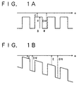
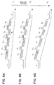
- Figure 1A shows a conduction band of a quantum-wave interference layer having a multi-layer structure with plural periods of a first layer W and a second layer B as a unit formed in an i-layer.
- a band gap of the second layer B is wider than that of the first layer W.
- Electrons conduct by an external electric field from left to right as shown by an arrow in FIGS. 1A and 1B. Among the electrons, those that exist near the bottom of the conduction band of the second layer B are likely to contribute to conduction. The electrons near the bottom of the conduction band of the second layer B has a kinetic energy E.
- the electrons in the first layer W have a kinetic energy E+V and are thus accelerated by the potential energy V due to the band gap difference between the first layer W and the second layer B.
- electrons that move from the first layer W to the second layer B are decelerated by the potential energy V and return to their original kinetic energy E in the second layer B.
- the kinetic energy of electrons in the conduction band is modulated by the potential energy due to the multi-layer structure.
- the wave length of the electron quantum-wave is calculated by Eqs. 1 and 2 using the kinetic energy of the electron.
- the multi-layer structure having two kinds of layers with band gaps different from each other enables to reflect quantum-wave of electrons which conduct in an i-layer effectively.
- FIGS. 1B and 3B show an energy level gradient occurring in the quantum-wave interference layer on the condition that the external voltage is applied to the i-layer. Then E+V and E, kinetic energies of the first layer W and the second layer B, respectively, are enlarged according to progress of the quantum-wave, and each thickness of the first layer W and the second layer B become apart from the most suitable condition to have an effective reflectivity.
- the thickness of the first layer W and the second layer B are determined for selectively reflecting the holes or the electrons, because of the difference in potential energy between the valence and the conduction bands, and the difference in effective mass of holes and electrons in the first layer W and the second layer B.
- the optimum thickness for reflecting electrons is not the optimum thickness for reflecting holes. Accordingly, holes do not exist in the i-layer when the applied voltage is small, and the i-layer is completely depleted with respect to holes.
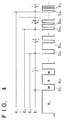
- Figure 4 shows a plurality quantum-wave interference units I k with arbitrary periods T k including a first layer having a thickness of D wk and a second layer having a thickness of D Bk and arranged in series, which are formed in an i-layer.
- E k , m Wk , m Bk , and n Wk and n Bk represent plural kinetic energy levels of carriers conducted into the second layer, effective mass of carriers with kinetic energy E k +V in the first layer, effective mass of carriers with kinetic energy E k in the second layer, and arbitrary odd numbers, respectively.
- the plurality of the partial quantum-wave interference layers I k are arranged in series from I 1 to I j , where j is a maximum number of k required to form a quantum-wave interference layer as a whole.
- a plural quantum-wave interference units having a plural layer structure is formed concatenated at an arbitrary interval, and a carrier accumulation layer is formed between each of the quantum-well interference layers to confine carriers. And in one aspect of the present invention, a bandwidth of the carrier accumulation layer is equal to that of the second layer.
- FIGS. 6A to 6C show a band structure of the i-layer.
- Each quantum-wave interference units A 1 to A 4 is formed at an arbitrary interval, and each carrier accumulation layers C 1 to C 3 is formed between the quantum-wave interference units. Electrons existing in the i-layer are confined effectively by the carrier accumulation layers C 1 to C 3 , and a capacity of the i-layer is enlarged.
- a quantum-wave wavelength of electrons existing in each quantum-wave interference units A 1 to A 4 does not satisfy a condition to reflect electrons, which are accelerated to flow by an electric field of the i-layer. Accordingly, an electron concentration of each carrier accumulation layers C 1 to C 3 is decreased, and the capacity of i-layer becomes smaller. Thus controlling the capacity is possible by applying an external voltage.
- FIGS. 6A to 6C show an example when an applied voltage is enlarged from V 1 to V 3 .
- the i-layer can be formed so that each quantum-wave interference units A 1 to A 4 has the biggest reflectivity at the predetermined applied voltage V.
- the capacity around the predetermined applied voltage V shows the largest value at this time.
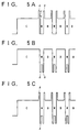
- the ninth aspect of the present invention is to form a ⁇ layer at the interface between the first layer W and the second layer B.
- the ⁇ layer has a thickness substantially thinner than both of the first layer W and the second layer B and sharply varies the energy band profile of the device.
- the reflectivity R of the interface is determined by Eq. 7.
- the ⁇ layer may be formed on both ends of every first layer W as shown in FIGS. 5A to 5C.
- the ⁇ layers are formed so that an energy level higher than that of the second layer B may be formed.
- the ⁇ layers are formed so that an energy level lower than that of the first layer W may be formed.
- the ⁇ layers are formed so that a band bottom higher than that of the second layer B and a band bottom lower than that of the first layer W may be formed.
- the ⁇ layer can be formed on one end of every first layer W.
- the i-layer can he an pip-type and carriers can be holes.
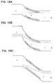
- FIGS. 10A to 10C show a conduction band of a quantum-wave interference layer having a multi-layer structure with plural periods of a first layer W and a second layer B as a unit formed in an n - -layer.
- a band gap of the second layer B is wider than that of the first layer W.
- Electrons conduct by an external electric field from left to right as shown by an arrow in FIGS. 1A and 1B. Among the electrons, those that exist near the bottom of the conduction band of the second layer B are likely to contribute to conduction.
- the electrons near the bottom of the conduction band the second layer B has a kinetic energy E. Accordingly, the electrons in the first layer W have a kinetic energy E+V and are thus accelerated by the potential energy V due to the band gap difference between the first layer W and the second layer B. In other words, electrons that move from the first layer W to the second layer B are decelerated by the potential energy V and return to their original kinetic energy E in the second layer B. As explained above, the kinetic energy of electrons in the conduction band is modulated by the potential energy due to the multi-layer structure.
- the wave length of the electron quantum-wave is calculated by Eqs. 3 and 4 using the kinetic energy of the electron.
- the multi-layer structure having two kinds of layers with band gaps different from each other enables to reflect quantum-wave of electrons which conduct in an n - -layer effectively.
- FIGS. 1B and 3B show an energy level gradient occurring in the quantum-wave interference layer on the condition that the external voltage is applied to the n - -layer.
- the thickness of the first layer W and the second layer B are determined for selectively reflecting the holes or the electrons, because of the difference in potential energy between the valence and the conduction bands, and the difference in effective mass of holes and electrons in the first layer W and the second layer B.
- the optimum thickness for reflecting electrons is not the optimum thickness for reflecting holes.
- a device having an nn - p structure is shown in the above aspects.
- a device having np - p or nip structure can be used.
- Figure 4 shows a plurality quantum-wave interference units I k with arbitrary periods T k including a first layer having a thickness of D wk and a second layer having a thickness of D Bk and arranged in series, which are formed in an n - layer, a p - layer, or an i-layer.
- E k , m Wk , m Bk , and n Wk and n Bk represent plural kinetic energy levels of carriers conducted into the second layer, effective mass of carriers with kinetic energy E k +V in the first layer, effective mass of carriers with kinetic energy E k in the second layer, and arbitrary odd numbers, respectively.
- the plurality of the partial quantum-wave interference layers I k are arranged in series from I 1 to I j , where j is a maximum number of k required to form a quantum-wave interference layer as a whole.
- a plurality of quantum-wave interference units having a plural layer structure is formed concatenated at an arbitrary interval, i.e., in series, and a carrier accumulation layer is formed between each of the quantum-well interference layers to confine carriers.
- a bandwidth of the carrier accumulation layer is equal to that of the second layer.
- FIGS. 11 and 15 show a band structure of the n - layer, the p - layer, or the i-layer.
- Each quantum-wave interference units G 1 to G 4 is formed at an arbitrary interval, and each carrier accumulation layers C 1 to C 3 is formed between the quantum-wave interference units. Electrons existing in the n - layer, the p - layer, or the i-layer are confined effectively by the carrier accumulation layers C 1 to C 3 , and a capacity of the device is enlarged.
- each quantum-wave interference unit G 1 to G 4 When an applied voltage is increased, a quantum-wave wavelength of electrons existing in each quantum-wave interference units G 1 to G 4 does not satisfy a condition to reflect electrons, which are accelerated to flow by an electric field of the n - layer, the p - layer, or the i-layer. Accordingly, an electron concentration of each carrier accumulation layers C 1 to C 3 is decreased, and the capacity of the n - layer, the p - layer, or the i-layer becomes smaller. Thus controlling the capacity is possible by applying an external voltage.
- FIGS. 11 and 15 show an example when an applied voltage is enlarged from V 1 to V 3 .
- the n - layer, the p - layer, or the i-layer can be formed so that each quantum-wave interference units G 1 to G 4 has the biggest reflectivity at the predetermined applied voltage V.
- the capacity around the predetermined applied voltage V shows the largest value at this time.
- the eighteenth aspect of the present invention is to form a ⁇ layer at the interface between the first layer W and the second layer B.
- the ⁇ layer has a thickness substantially thinner than both of the first layer W and the second layer B and sharply varies the energy band profile of the device.
- the reflectivity R of the interface is determined by Eq. 15.
- the ⁇ layer may be formed on both ends of every first layer W as shown in FIGS. 5A to 5C.
- the ⁇ layers are formed so that an energy level higher than that of the second layer B may be formed.
- the ⁇ layers are formed so that an energy level lower than that of the first layer W may be formed.
- the ⁇ layers are formed so that a band bottom higher than that of the second layer B and a band bottom lower than that of the first layer W may be formed.
- the ⁇ layer can be formed on one end of every first layer W.
- This explanation is applied to a device having an nn - p, np - p, or nip structure. And it is applicable to the case that holes are conduction carriers.
- FIG. 7 is a sectional view of a variable capacity device 100 in which a quantum-wave interference layer is formed in an i-layer.
- the variable capacity device 100 has a substrate 10 made of gallium arsenide (GaAs).
- GaAs buffer layer 12 of n-type conduction having a thickness generally of 0.3 ⁇ m and an electron concentration of 2 x 10 18 /cm 3 , is formed on the substrate 10.
- n-Al 0.51 In 0.49 P n-layer 16 of n-type conduction having a thickness generally of 0.2 ⁇ m and an electron concentration of 1 x 10 18 /cm 3 , is formed on the contact layer 14.
- a non-doped i-layer 18 is formed on the n-layer 16.
- a Al 0.51 In 0.49 P n-layer 20 of n-type conduction having a thickness generally of 0.2 ⁇ m and an electron concentration of 1 x 10 18 /cm 3 , is formed on the i-layer 18.
- a n-Ga 0.51 In 0.49 P second contact layer 22 of n-type conduction having a thickness generally of 0.13 ⁇ m and an electron concentration of 2 x 10 18 /cm 3 , is formed on the n-layer 20.
- An n-GaAs first contact layer 24 of n-type conduction having a thickness generally of 0.06 ⁇ m and an electron concentration of 2 x 10 18 /cm 3 , is formed on the second contact layer 22.
- FIGS. 8A to 8C show band structures of the quantum-wave interference layer A 1 in detail.
- the first layer W has a thickness of 5 nm
- the second layer B has a thickness of 7 nm.
- a non-doped ⁇ layer made of Al 0.33 Ga 0.33 In 0.33 P is formed at each interface between the first layer W and the second layer B.
- Non-doped Al 0.51 In 0.49 P carrier accumulation layers C 1 to C 3 having a thickness of 177 nm, is formed between any quantum-wave interference units A i and A i+1 , respectively, as shown in Figure 7. Thicknesses of the first layer W and the second layer are determined according to Eqs. 1 and 2, respectively, on condition that no external voltage is applied thereto.
- the second layers B which contact to the n-layer 20 and the p-layer 16 have a thickness of 0.05 ⁇ m, respectively.
- the substrate 10 has a diameter of 2.0 inches and the normal direction of its main surface is offset toward the [011] axis by 15 degree from the (100) plane.
- the voltage-variable capacity device 100 was manufactured by gas source molecular beam epitaxial deposition (GS-MBE) which is an epitaxial growth method under extremely high vacuum condition.
- GS-MBE is different from a conventional MBE which supplies group III and V elements both from said state sources.
- group III elements such as indium (In), gallium (Ga), and aluminum (Al) are supplied from a solid source and group V elements such as arsenic (As) and phosphorous (P) are supplied by heat decomposition of gas material such as AsH 3 and PH 3 .
- Figure 6A shows an electric potential gradient occurring in the i-layer 18 as an insulation layer on the condition that an external voltage is applied to the interface between the n-layer 20 and the n-layer 16 of the variable capacity device 100.
- the ⁇ layer is not shown in FIGS. 6A to 6C, it is present at each interface between the first layer W and the second layer B, as shown in FIGS. 8A to 8C.
- Each quantum-wave interference units A 1 to A 4 reflects electrons when the external voltage is in the range of 0 to V 1 as shown in Figure 6A.
- electrons which exists in the i-layer 18 are not conducted in the i-layer and are confined in each carrier accumulation layers C 1 to C 3 , respectively.
- an effective thickness of a depletion layer is smaller, and an electrostatic capacity between the electrodes 26 and 28 is larger.
- each quantum-well interference layers A 1 to A 4 reflects electrons. Accordingly, electrons are conducted and a electron concentration of each carrier accumulation layers C 1 to C 3 is decreased. Because each carrier accumulation layers C 1 to C 3 becomes a depletion layer, which means that equivalently the thickness of the depletion layer in the i-layer 18 becomes larger, the capacity of the variable capacity device 100 decreases. Thus by applying a larger applied voltage V, the capacity can be decreased.
- Capacity value with respect to an alternating current when a voltage V was applied as a bias voltage was measured by varying the respective value of the applied voltage V.
- Figure 9 shows a result when the alternating currents are fixed at 100 kHz and 1 MHz, respectively.
- a characteristics X shows a curve when the alternating current is 1 MHz. When the applied voltage V is over 0.6 V, the capacity value of X suddenly drops.
- a characteristics Y shows a curve when the alternating current is 100 kHz. A peak of capacity value of Y is obtained when the applied voltage V is 0.7 V.
- a characteristics Z shows a curve of a voltage-variable capacity device in the prior art.
- plurality of partial quantum-wave interference layers can be constructed with serial pairs of T 1 to T j to obtain the characteristics of a voltage-capacity.
- a ⁇ layer is formed in the device 100.
- the ⁇ layer improves a reflectivity at the interface between the first layer W and the second layer B.
- the ⁇ layer is not necessarily needed.
- quantum-wave interference units A 1 to A 4 are connected in series, with a carrier accumulation layer C lying between each of the quantum-wave interference units.
- one quantum-wave interference layer can be made in an i-layer.
- the quantum-wave interference layer was formed to have a multi-layer structure including Ga 0.51 In 0.49 P and Al 0.51 In 0.49 P.
- the quantum-wave interference layer can be made of two combinations of quaternary compounds such as Al x Ga y In 1-x-y P, selecting different arbitrary composition ratio within the range of 0 ⁇ x ⁇ 1, 0 ⁇ y ⁇ 1, and 0 ⁇ x+y ⁇ 1.
- the quantum-wave interference layer can be made of arbitrary group III-V compound semiconductor, group II-VI compound semiconductor, Si and Ge, and semiconductors of other hetero-material.
- an i-layer is a non-doped layer.
- a small amount of donor impurity or acceptor impurity can be doped with the i-layer.
- pip structure can be used in which i-layer has a quantum-wave interference layer with respect to holes.
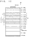
- Figure 12 is a sectional view of a variable capacity device 200 in which a quantum-wave interference layer is formed in a n - -type layer.
- the variable capacity has a substrate 110 made of gallium arsenide (GaAs).
- GaAs buffer layer 112 of n-type conduction having a thickness generally of 0.3 ⁇ m and an electron concentration of 2 x 10 18 /cm 3 , is formed on the substrate 110.
- An n-Ga 0.51 In 0.49 P contact layer 114 of n-type conduction having a thickness generally of 0.13 ⁇ m and an electron concentration of 2 x 10 18 /cm 3 , is formed on the buffer layer 112.
- n-Al 0.51 In 0.49 P n-layer 116of n-type conduction having a thickness generally of 0.2 ⁇ m and an electron concentration of 1 x 10 18 /cm 3 , is formed on the contact layer 114.
- An n - layer 118 having an electron concentration which becomes smaller in accordance with approaching to a p-layer 120, is formed.
- the p-Al 0.51 In 0.49 P p-layer 120 of p-type conduction having a thickness generally of 0.2 ⁇ m and a hole concentration of 1 x 10 18 /cm 3 , is formed on the n - layer 118.
- a p-Ga 0.51 In 0.49 P second contact layer 122 of p-type conduction having a thickness generally of 0.13 ⁇ m and a hole concentration of 2 x 10 18 /cm 3 , is formed on the p-layer 120.
- a p-GaAs first contact layer 124 of p-type conduction having a thickness generally of 0.06 ⁇ m and a hole concentration of 2 x 10 18 /cm 3 , is formed on the second contact layer 122.
- the n - layer 118 has an electron concentration of 3 x 10 16 /cm 3 .
- a quantum-wave interference layer G 1 having a multi-quantum layer structure with 12 pairs of a Ga 0.51 In 0.49 P first layer W and an Al 0.51 In 0.49 P second layer B is formed in the n - layer 118.
- G 2 , ... G 5 are formed like G 1 , and 5 quantum-wave interference units in total are formed in the n - layer 118.
- FIGS. 8A to 8C shows a structure of the quantum-wave interference layer G 1 in detail.
- the first layer W has a thickness of 5 nm
- the second layer B has a thickness of 7nm.
- a non-doped Al 0.51 In 0.49 P carrier accumulation layers C 1 to C 4 having a thickness of 14 nm, is formed between any quantum-wave interference units G 1 and G i+1 , respectively, as shown in Figure 11.
- a thickness of the first layer W and that of the second layer B are determined according to Eqs. 3 and 4, respectively, on condition that no external voltage is applied thereto.
- the second layers B which contact to the p-layer 120 and the n-layer 116 have a thickness of 0.05 ⁇ m, respectively.
- the substrate 110 has a diameter of 2.0 inches and the normal direction of its main surface is offset toward the [011] axis by 15 degree from the (100) plane.
- the variable capacity device 200 was manufactured by gas source molecular beam epitaxial deposition (GS-MBE) which is an epitaxial growth method under extremely high vacuum condition.
- GS-MBE is different from a conventional MBE which supplies group III and V elements both from solid state sources.
- group III elements such as indium (In), gallium (Ga), and aluminum (Al) are supplied from a solid source and group V elements such as arsenic (As) and phosphorus (P) are supplied by heat decomposition of gas material such as AsH 3 and PH 3 .
- MOCVD metal organic chemical vapor deposition
- Figure 11A shows an electric potential gradient occurring in the n - -layer 118 because of a higher resistivity compared with the p-layer 120 or n-layer 116 on the condition that a backward voltage is applied to the interface between the p-layer 120 and the n-layer 116 of the variable capacity device 200.
- the ⁇ layer is not shown in FIGS. 11A to 11C, it is present at each interface between the first layer W and the second layer B, as shown in FIGS. 8A to 8C.
- FIGS. 8A to 8C Although only two carrier accumulation layers C 1 and C 2 are shown in FIGS. 11A to 11C, four exist from C 1 to C 4 .
- FIGS. 11A to 11C Although only five pairs of layers in each of quantum-wave interference units are shown in FIGS. 11A to 11C, they exist in twelve pairs.
- Each quantum-wave interference units G 1 to G 5 reflects electrons when an external voltage is in the range of 0 to V 1 as shown in Figure 11A. At this stage, electrons which exists in the n - -layer 118 are not conducted in the n - -layer 118 and are confined in each carrier accumulation layers C 1 to C 4 , respectively. As a result, an effective thickness of a depletion layer is smaller, and an electrostatic capacity between the electrodes 126 and 128 is larger.
- each quantum-well interference layers G 1 to G 5 reflects electrons. Accordingly, electrons are conducted and a electron concentration of each carrier accumulation layers C 1 to C 4 is decreased. Because each carrier accumulation layers C 1 to C 4 becomes a depletion layer, which means that equivalently the thickness of the depletion layer in the n - -layer 118 becomes larger, the capacity of the variable capacity device 200 decreases. Thus by applying a larger applied voltage V, the capacity can be decreased.
- Capacity value with respect to alternating current when a voltage V was applied as a bias voltage was measured by varying the respective value of the applied voltage V.
- Figure 13 shows a result when the alternating current is fixed at 100 kHz and 1 MHz.
- a characteristics X shows a curve when the alternating current is 1 MHz.
- a characteristics Y shows a curve when the alternating current is 100 kHz.
- a characteristics Z shows a curve of a voltage-variable capacity device in the prior art.
- the applied voltage V is over 1.0 V, the decrease of capacity value Z is saturated.
- a dynamic range of variable capacity of the present invention is wider compared with that of the prior art, although a voltage-variation rate of capacity becomes smaller.
- a variable capacity device has a structure as same as that of the variable capacity device 200 of Figure 12.
- a thickness of each carrier accumulation layers C 1 to C 4 is duplicated to 8 nm and a measured capacity is shown in Figure 14. Comparing Figure 13 with Figure 14, a voltage-variation rate of capacity becomes smaller in accordance with a thickness of each carrier accumulation layers C 1 to C 4 being larger. The dynamic range of capacity of both obtained devices are improved to be wider compared with that of the prior art.
- a ⁇ layer is formed in the device 200.
- the ⁇ layer improves a reflectivity at the interface between the first layer W and the second layer B.
- the ⁇ layer is not necessarily needed.
- five quantum-wave interference units G 1 to G 5 are connected in series, with a carrier accumulation layer C lying between each of the quantum-wave interference units.
- one quantum-wave interference layer can be made in an n - layer without forming a carrier accumulation layer C.
- Number of the quantum-wave interference units of a multi-layer structure is arbitrary.
- the quantum-wave interference layer was formed to have a multi-layer structure including Ga 0.51 In 0.49 P and Al 0.51 In 0.49 P.
- the quantum-wave interference layer can be made of two combinations of quaternary compounds such as Al x Ga y In 1-x-y P, selecting different arbitrary composition ratio within the range of 0 ⁇ x ⁇ 1, 0 ⁇ y ⁇ 1, and 0 ⁇ x+y ⁇ 1.
- the quantum-wave interference layer can be made of group III-V compound semiconductor, arbitrary group II-VI compound semiconductor, Si and Ge, and semiconductors of other hetero-material.
- a variable capacity having an nn - p junction structure is shown.
- a quantum-wave interference layer which interferes quantum-waves of holes, can be formed in the p - layer of an np - p junction structure.
- a quantum-wave interference layer which interferes quantum-waves of electrons or holes, can be formed in the i-layer of an nip structure.
- quantum-wave interference units which interfere quantum-waves of electrons and holes, respectively, can be formed in the i-layer of the nip structure.
- Figure 15 shows a conduction band of a variable capacity device, having a pin structure.
- a quantum-wave interference layer of electrons is formed in an i-layer of the device. According to a backward voltage applied to the device being larger, carriers which exist in carrier accumulation layers decrease, and according to a thickness of a depletion layer being larger, a capacity becomes smaller.
- a variable capacity device having an nin, pip, nn - p, np - p, or nip junction whose middle layer is constituted by a quantum-wave interference layer with plural periods of a first layer W and a second layer B as a unit.
- the second layer B has a wider band gap than the first layer W.
- Each thickness of the first layer W and the second layer B is determined by multiplying by an odd number one fourth of a wavelength of a quantum-wave of carriers in each of the first layer W and the second layer B existing around the lowest energy level of the second layer B.
- a ⁇ layer for changing energy band suddenly, is formed at interfaces between the first layer W and the second layer B and has a thickness substantially thinner than the first layer W and the second layer B.
- Plurality of quantum-wave interference units are formed sandwiching carrier accumulation layers in series. Then a voltage-variation rate of capacity of the variable capacity device is improved.
Landscapes
- Engineering & Computer Science (AREA)
- Chemical & Material Sciences (AREA)
- Nanotechnology (AREA)
- Physics & Mathematics (AREA)
- Mathematical Physics (AREA)
- Theoretical Computer Science (AREA)
- Crystallography & Structural Chemistry (AREA)
- Optical Modulation, Optical Deflection, Nonlinear Optics, Optical Demodulation, Optical Logic Elements (AREA)
Applications Claiming Priority (4)
| Application Number | Priority Date | Filing Date | Title |
|---|---|---|---|
| JP4107398A JP3014359B2 (ja) | 1998-02-06 | 1998-02-06 | 量子波干渉層を有した可変容量素子 |
| JP4107398 | 1998-02-06 | ||
| JP6049498 | 1998-02-24 | ||
| JP10060494A JP3014361B2 (ja) | 1998-02-24 | 1998-02-24 | 量子波干渉層を有した可変容量素子 |
Publications (1)
| Publication Number | Publication Date |
|---|---|
| EP0935294A1 true EP0935294A1 (fr) | 1999-08-11 |
Family
ID=26380609
Family Applications (1)
| Application Number | Title | Priority Date | Filing Date |
|---|---|---|---|
| EP99102297A Withdrawn EP0935294A1 (fr) | 1998-02-06 | 1999-02-05 | Dispositif à capacité variable comportant des couches à interference d'ondes quantiques |
Country Status (2)
| Country | Link |
|---|---|
| US (1) | US6331716B1 (fr) |
| EP (1) | EP0935294A1 (fr) |
Cited By (2)
| Publication number | Priority date | Publication date | Assignee | Title |
|---|---|---|---|---|
| EP0964452A3 (fr) * | 1998-05-26 | 2000-01-26 | Canare Electric Co., Ltd. | Dispositif semi-conducteur comprenant des couches à interférences d'ondes quantiques |
| EP0996166A3 (fr) * | 1998-10-21 | 2003-11-05 | Canare Electric Co., Ltd. | Dispositifs semi-conducteurs comprenant une structure de barrière quantique multiple |
Families Citing this family (2)
| Publication number | Priority date | Publication date | Assignee | Title |
|---|---|---|---|---|
| US7696604B2 (en) * | 2007-10-23 | 2010-04-13 | International Business Machines Corporation | Silicon germanium heterostructure barrier varactor |
| US9893212B2 (en) | 2011-11-08 | 2018-02-13 | International Business Machines Corporation | Quantum capacitance graphene varactors and fabrication methods |
Citations (9)
| Publication number | Priority date | Publication date | Assignee | Title |
|---|---|---|---|---|
| EP0272885A2 (fr) * | 1986-12-20 | 1988-06-29 | Fujitsu Limited | Dispositif semi-conducteur comportant une diode de décalage de niveau |
| EP0471288A2 (fr) * | 1990-08-09 | 1992-02-19 | Canon Kabushiki Kaisha | Dispositifs de couplage ou de découplage d'ondes électroniques et dispositifs à interférences quantiques |
| US5091756A (en) * | 1986-08-14 | 1992-02-25 | Tokyo Institute Of Technology | Superlattice structure |
| EP0485237A2 (fr) * | 1990-11-09 | 1992-05-13 | Furukawa Electric Co., Ltd. | Dispositif optique à semi-conducteur à couche de barrière quantique |
| EP0569258A2 (fr) * | 1992-05-08 | 1993-11-10 | The Furukawa Electric Co., Ltd. | Dispositif à jonction Schottky ayant une barrière quantique multiple |
| US5278444A (en) * | 1992-02-26 | 1994-01-11 | The United States Of America As Represented By The Administrator Of The National Aeronautics And Space Administration | Planar varactor frequency multiplier devices with blocking barrier |
| US5336923A (en) * | 1992-12-31 | 1994-08-09 | Honeywell, Inc. | Varactor diode having a stepped capacitance-voltage profile |
| EP0874402A1 (fr) * | 1997-04-25 | 1998-10-28 | Canare Electric Co. Ltd. | Diodes présentant des couches d'interference d'ondes quantiques |
| EP0874403A2 (fr) * | 1997-04-25 | 1998-10-28 | Canare Electric Co. Ltd. | Dispositifs semi-conducteurs avec des couches d'interférences à ondes quantiques |
Family Cites Families (2)
| Publication number | Priority date | Publication date | Assignee | Title |
|---|---|---|---|---|
| EP0506127B1 (fr) * | 1991-03-28 | 1999-06-09 | Nec Corporation | Photodétecteur à semi-conducteur utilisant la multiplication par avalanche |
| JPH0888434A (ja) * | 1994-09-19 | 1996-04-02 | Mitsubishi Electric Corp | 半導体レーザ,及びその製造方法 |
-
1999
- 1999-02-05 US US09/245,299 patent/US6331716B1/en not_active Expired - Fee Related
- 1999-02-05 EP EP99102297A patent/EP0935294A1/fr not_active Withdrawn
Patent Citations (9)
| Publication number | Priority date | Publication date | Assignee | Title |
|---|---|---|---|---|
| US5091756A (en) * | 1986-08-14 | 1992-02-25 | Tokyo Institute Of Technology | Superlattice structure |
| EP0272885A2 (fr) * | 1986-12-20 | 1988-06-29 | Fujitsu Limited | Dispositif semi-conducteur comportant une diode de décalage de niveau |
| EP0471288A2 (fr) * | 1990-08-09 | 1992-02-19 | Canon Kabushiki Kaisha | Dispositifs de couplage ou de découplage d'ondes électroniques et dispositifs à interférences quantiques |
| EP0485237A2 (fr) * | 1990-11-09 | 1992-05-13 | Furukawa Electric Co., Ltd. | Dispositif optique à semi-conducteur à couche de barrière quantique |
| US5278444A (en) * | 1992-02-26 | 1994-01-11 | The United States Of America As Represented By The Administrator Of The National Aeronautics And Space Administration | Planar varactor frequency multiplier devices with blocking barrier |
| EP0569258A2 (fr) * | 1992-05-08 | 1993-11-10 | The Furukawa Electric Co., Ltd. | Dispositif à jonction Schottky ayant une barrière quantique multiple |
| US5336923A (en) * | 1992-12-31 | 1994-08-09 | Honeywell, Inc. | Varactor diode having a stepped capacitance-voltage profile |
| EP0874402A1 (fr) * | 1997-04-25 | 1998-10-28 | Canare Electric Co. Ltd. | Diodes présentant des couches d'interference d'ondes quantiques |
| EP0874403A2 (fr) * | 1997-04-25 | 1998-10-28 | Canare Electric Co. Ltd. | Dispositifs semi-conducteurs avec des couches d'interférences à ondes quantiques |
Non-Patent Citations (4)
| Title |
|---|
| LHEURETTE E ET AL: "HIGH PERFORMANCE INP-BASED HETEROSTRUCTURE BARRIER VARACTORS IN SINGLE AND STACK CONFIGURATION", ELECTRONICS LETTERS, vol. 32, no. 15, 18 July 1996 (1996-07-18), pages 1417/1418, XP000625459 * |
| MASAMICHI YAMANISHI: "ULTRAFAST MODULATION OF QUANTUM STATES BY VIRTUAL CHARGE POLARIZATION IN BIASED QUANTUM WELL STRUCTURES", SUPERLATTICES AND MICROSTRUCTURES, vol. 6, no. 4, 1 January 1989 (1989-01-01), pages 403 - 408, XP000147831 * |
| RAHAL A ET AL: "PLANAR MULTI-STACK QUANTUM BARRIER VARACTOR TRIPLER EVALUATION AT W-BAND", ELECTRONICS LETTERS, vol. 31, no. 23, 9 November 1995 (1995-11-09), pages 2022/2023, XP000546738 * |
| TAKESHI TAKAGI ET AL: "POTENTIAL BARRIER HEIGHT ANALYSIS OF ALGAINP MULTI-QUANTUM BARRIER (MQB)", JAPANESE JOURNAL OF APPLIED PHYSICS, vol. 29, no. 11, 1 November 1990 (1990-11-01), pages L1977 - L1980, XP000224038 * |
Cited By (3)
| Publication number | Priority date | Publication date | Assignee | Title |
|---|---|---|---|---|
| EP0964452A3 (fr) * | 1998-05-26 | 2000-01-26 | Canare Electric Co., Ltd. | Dispositif semi-conducteur comprenant des couches à interférences d'ondes quantiques |
| US6552412B2 (en) | 1998-05-26 | 2003-04-22 | Canare Electric Co., Ltd. | Semiconductor device with quantum-wave interference layers |
| EP0996166A3 (fr) * | 1998-10-21 | 2003-11-05 | Canare Electric Co., Ltd. | Dispositifs semi-conducteurs comprenant une structure de barrière quantique multiple |
Also Published As
| Publication number | Publication date |
|---|---|
| US6331716B1 (en) | 2001-12-18 |
Similar Documents
| Publication | Publication Date | Title |
|---|---|---|
| EP0616400B1 (fr) | Laser à semi-conducteur | |
| US6175123B1 (en) | Semiconductor devices with quantum-wave interference layers | |
| JPH065784B2 (ja) | アバランシエ光検出器 | |
| US6664561B2 (en) | Light-receiving device with quantum-wave interference layers | |
| US6331716B1 (en) | Variable capacity device with quantum-wave interference layers | |
| JP3604400B2 (ja) | 半導体レーザ素子 | |
| US6188083B1 (en) | Diodes with quantum-wave interference layers | |
| US6552412B2 (en) | Semiconductor device with quantum-wave interference layers | |
| US6188082B1 (en) | Diodes with quantum-wave interference layers | |
| EP1130722B1 (fr) | Dispositif laser à semiconducteur | |
| US6479842B1 (en) | Field effect transistor with a quantum-wave interference layer | |
| EP0967658A2 (fr) | Dispositif semi-conducteur avec des couches d'interférences à ondes quantiques | |
| JP3014361B2 (ja) | 量子波干渉層を有した可変容量素子 | |
| EP0996169A2 (fr) | Dispositif semi-conducteur avec une couche de confinement | |
| US6818916B2 (en) | Light-receiving device with quantum-wave interference layers | |
| JP3014359B2 (ja) | 量子波干渉層を有した可変容量素子 | |
| US6486490B1 (en) | Light-emitting device with a quantum-wave interference layer | |
| US6337508B1 (en) | Transistor with a quantum-wave interference layer | |
| EP0996166A2 (fr) | Dispositifs semi-conducteurs comprenant une structure de barrière quantique multiple | |
| JP2001284728A (ja) | 半導体レーザ素子 | |
| JPH06216457A (ja) | 光電素子 |
Legal Events
| Date | Code | Title | Description |
|---|---|---|---|
| PUAI | Public reference made under article 153(3) epc to a published international application that has entered the european phase |
Free format text: ORIGINAL CODE: 0009012 |
|
| AK | Designated contracting states |
Kind code of ref document: A1 Designated state(s): DE FR GB |
|
| AX | Request for extension of the european patent |
Free format text: AL;LT;LV;MK;RO;SI |
|
| 17P | Request for examination filed |
Effective date: 20000121 |
|
| AKX | Designation fees paid |
Free format text: DE FR GB |
|
| STAA | Information on the status of an ep patent application or granted ep patent |
Free format text: STATUS: THE APPLICATION IS DEEMED TO BE WITHDRAWN |
|
| 18D | Application deemed to be withdrawn |
Effective date: 20050901 |