EP0945968A2 - Boost converter having extended holdup time and method of operation thereof - Google Patents
Boost converter having extended holdup time and method of operation thereof Download PDFInfo
- Publication number
- EP0945968A2 EP0945968A2 EP99302032A EP99302032A EP0945968A2 EP 0945968 A2 EP0945968 A2 EP 0945968A2 EP 99302032 A EP99302032 A EP 99302032A EP 99302032 A EP99302032 A EP 99302032A EP 0945968 A2 EP0945968 A2 EP 0945968A2
- Authority
- EP
- European Patent Office
- Prior art keywords
- holdup
- capacitor
- boost converter
- output
- input
- Prior art date
- Legal status (The legal status is an assumption and is not a legal conclusion. Google has not performed a legal analysis and makes no representation as to the accuracy of the status listed.)
- Withdrawn
Links
- 238000000034 method Methods 0.000 title claims abstract description 15
- 239000003990 capacitor Substances 0.000 claims abstract description 107
- 238000004146 energy storage Methods 0.000 claims abstract description 28
- 230000000087 stabilizing effect Effects 0.000 claims abstract description 12
- 230000008878 coupling Effects 0.000 claims 1
- 238000010168 coupling process Methods 0.000 claims 1
- 238000005859 coupling reaction Methods 0.000 claims 1
- 238000010586 diagram Methods 0.000 description 8
- 238000006243 chemical reaction Methods 0.000 description 3
- 230000001052 transient effect Effects 0.000 description 3
- 230000009471 action Effects 0.000 description 2
- 230000001627 detrimental effect Effects 0.000 description 2
- 230000004308 accommodation Effects 0.000 description 1
- 230000004075 alteration Effects 0.000 description 1
- 230000015556 catabolic process Effects 0.000 description 1
- 230000008859 change Effects 0.000 description 1
- 239000004020 conductor Substances 0.000 description 1
- 238000010276 construction Methods 0.000 description 1
- 230000007812 deficiency Effects 0.000 description 1
- 238000006731 degradation reaction Methods 0.000 description 1
- 230000000694 effects Effects 0.000 description 1
- 238000001914 filtration Methods 0.000 description 1
- 230000008569 process Effects 0.000 description 1
- 230000001105 regulatory effect Effects 0.000 description 1
- 238000006467 substitution reaction Methods 0.000 description 1
Images


Classifications
-
- H—ELECTRICITY
- H02—GENERATION; CONVERSION OR DISTRIBUTION OF ELECTRIC POWER
- H02M—APPARATUS FOR CONVERSION BETWEEN AC AND AC, BETWEEN AC AND DC, OR BETWEEN DC AND DC, AND FOR USE WITH MAINS OR SIMILAR POWER SUPPLY SYSTEMS; CONVERSION OF DC OR AC INPUT POWER INTO SURGE OUTPUT POWER; CONTROL OR REGULATION THEREOF
- H02M1/00—Details of apparatus for conversion
- H02M1/42—Circuits or arrangements for compensating for or adjusting power factor in converters or inverters
- H02M1/4208—Arrangements for improving power factor of AC input
-
- H—ELECTRICITY
- H02—GENERATION; CONVERSION OR DISTRIBUTION OF ELECTRIC POWER
- H02M—APPARATUS FOR CONVERSION BETWEEN AC AND AC, BETWEEN AC AND DC, OR BETWEEN DC AND DC, AND FOR USE WITH MAINS OR SIMILAR POWER SUPPLY SYSTEMS; CONVERSION OF DC OR AC INPUT POWER INTO SURGE OUTPUT POWER; CONTROL OR REGULATION THEREOF
- H02M1/00—Details of apparatus for conversion
- H02M1/0096—Means for increasing hold-up time, i.e. the duration of time that a converter's output will remain within regulated limits following a loss of input power
-
- Y—GENERAL TAGGING OF NEW TECHNOLOGICAL DEVELOPMENTS; GENERAL TAGGING OF CROSS-SECTIONAL TECHNOLOGIES SPANNING OVER SEVERAL SECTIONS OF THE IPC; TECHNICAL SUBJECTS COVERED BY FORMER USPC CROSS-REFERENCE ART COLLECTIONS [XRACs] AND DIGESTS
- Y02—TECHNOLOGIES OR APPLICATIONS FOR MITIGATION OR ADAPTATION AGAINST CLIMATE CHANGE
- Y02B—CLIMATE CHANGE MITIGATION TECHNOLOGIES RELATED TO BUILDINGS, e.g. HOUSING, HOUSE APPLIANCES OR RELATED END-USER APPLICATIONS
- Y02B70/00—Technologies for an efficient end-user side electric power management and consumption
- Y02B70/10—Technologies improving the efficiency by using switched-mode power supplies [SMPS], i.e. efficient power electronics conversion e.g. power factor correction or reduction of losses in power supplies or efficient standby modes
Definitions
- the present invention is directed, in general, to power conversion and, more specifically, to a boost converter having an extended holdup time and a method of operation thereof.
- Boost converters have been widely used in various power conversion applications such as single phase and three phase power factor corrected AC/DC switch-mode rectifiers.
- the boost stage processes the AC input and develops a DC output voltage that is typically between 400 volts and 800 volts.
- Boost converters are usually the topology of choice for providing a high output voltage from substantially lower DC voltages derived from sinusoidal input voltages.
- Boost converters are often used to supply power to computer or telecommunication systems that require power which is both clean and well regulated. If the power is interrupted, these systems usually require a "shut down" period in which to orderly prepare themselves. This period varies with application and should assure that an orderly shut down is completed.
- Boost converters employ various schemes that allow them to maintain their output voltage for a period of time after the input power has failed.
- One of the more prevalent "holdup" schemes is to use a large output capacitor that stores sufficient energy to maintain the output voltage above a minimum level for a specified period of time. For certain applications, this scheme requires prohibitively large capacitors in terms of size.
- Another scheme to maintain boost converter output voltage during holdup operation is to use a collection of switches to connect a portion of the output capacitance across the boost converter input during holdup mode operation. This allows the boost circuitry to transfer energy stored in this capacitance to the boost converter output thereby maintaining the output voltage for a period of time.
- Boost converters must also deal successfully with several other detrimental operational characteristics.
- Inrush is the potentially damaging initial, transient current that may flow into the boost converter when the AC power is first turned on.
- an inrush current that is not limited in some way is typically much larger than the currents which flow during normal, steady-state operation. This unlimited inrush current may cause circuit element damage unless more robust components are selected to accommodate these larger values of transient current which normally leads to sacrifices in either component cost or size.
- the nature of the boost converter design itself may allow for limiting or accommodation of the inrush current.
- the present invention provides, for use in a boost converter having a boost inductor coupled between an input and an output of the boost converter and an output capacitor coupled between rails of the output, an energy storage circuit for, and method of, extending a holdup time of the boost converter.
- the energy storage circuit includes: (1) a holdup capacitor coupled to a first rail of the input, (2) a holdup switch, coupled to a second rail of the input and the holdup capacitor, capable of closing during a holdup mode to allow the holdup capacitor to discharge current into the input and (3) a voltage stabilizing circuit, coupled between the holdup capacitor and the output capacitor, that: (3a) when the boost converter is in a normal mode, provides a substantially impeded path for charge current to flow from the output capacitor to charge the holdup capacitor, and (3b) when the boost converter is in an initial phase of the holdup mode, provides a substantially unimpeded path for holdup current to flow from the holdup capacitor to the output capacitor prior to the closing of the holdup switch.
- the present invention therefore introduces the broad concept of providing a holdup capacitor that is only conditionally coupled to the output capacitor (by way of the voltage stabilizing circuit) and that is couplable to the boost converter's input to increase holdup time.
- a “substantially impeded path,” as that phrase is employed herein, is defined as a path that presents a resistance to current flow sufficient to impede more than a current level necessary to charge the holdup capacitor.
- a “substantially unimpeded path” is capable of conducting more than a current level necessary to charge the output capacitor.
- the voltage stabilizing circuit comprises: (1) a discrete resistor that provides the substantially impeded path for the charge current and (2) a diode, coupled in parallel with the discrete resistor, that provides the substantially unimpeded path for the holdup current.
- the discrete resistor is replaced with a conductor that presents an impedance along its length. Although the diode may present some impedance to current flow, it is not substantial.
- the holdup switch forms a portion of an inrush current limiting circuit in the boost converter.
- Those skilled in the art are familiar with the structure and function of inrush current limiting circuits in the environment of boot converters.
- the holdup switch of the present invention can be advantageously integrated into an inrush current limiting circuit to yield a circuit having both functions with fewer components.
- the holdup switch forms a portion of a surge bypass circuit in the boost converter.
- Those skilled in the art are familiar with the structure and function of surge bypass circuits in the environment of boot converters.
- the energy storage circuit of the present invention can be advantageously integrated into a surge bypass circuit to yield a circuit having both functions with fewer components.
- a diode in the bypass circuit diverts at least a portion of surge current toward the output capacitor. In this embodiment, at least some of the energy in the surge can be recovered by the output capacitor. In a related, but alternative embodiment, a diode in the bypass circuit diverts at least a portion of surge current toward the holdup capacitor allowing it to participate along with the output capacitor as well.
- a bridge rectifier provides DC power to the input.
- the bridge rectifier may be single or multiple phase.
- Those skilled in the art are familiar with the structure and function of bridge rectifiers and their use with boost converters.
- the boost converter 100 includes an input bridge rectifier employing a plurality of diodes 101, 102, 103, 104, a boost inductor 105, a boost switch 106, a boost diode 107 and an output capacitor 108.
- the holdup circuit includes a holdup capacitor 109 and first and second holdup switches 110, 111.
- the first holdup switch 110 is open and the second holdup switch 111 is closed. This places the holdup capacitor 109 in parallel with the output capacitor 108.
- the holdup capacitor 109 charges to the same voltage as the output capacitor 108 and provides additional filtering for the output in the normal operating mode.
- control circuitry activates a holdup mode of operation for the boost converter 100 by closing the first holdup switch 110 and opening the second holdup switch 111. This action separates the two capacitors 108, 109 and places the holdup capacitor 109 across the input rails IR1, IR2 of the boost converter 100.
- the holdup capacitor 109 connected across the input rails IR1, IR2 may be discharged to a much lower voltage (almost fully discharged) while keeping the output voltage above the minimum value allowed by the DC/DC converter (fed by the boost converter) for proper operation, due to the nature of the boost conversion itself.
- This technique of switching part of the output capacitance to the input rails IR1, IR2 allows the output capacitor 108 to be smaller in value for a given power and holdup time than would be otherwise necessary. For example, for a power of 400 watts, a holdup time of 100 milliseconds and an output voltage degradation from 400 volts to 360 volts, a single output capacitance value of 2.63 millifarads (2,630 microfarads) would be required which is very large from a practical standpoint.
- Using an output capacitor 108 in conjunction with a separate holdup capacitor 109 under the assumption that they are equal in value for the conditions stated above yields a total value of 0.84 millifarads, less than one third of the previous capacitance value above.
- the prior art holdup circuit provides an adequate solution for holdup operation of a boost converter, multiple switching devices (namely, the first and second holdup switches 110, 111) are required and the prior art holdup circuit does not address other circuit concerns such as inrush currents.
- FIGURE 2 illustrated is a schematic diagram of a boost converter 200 employing an embodiment of an energy storage circuit constructed according to the principles of the present invention.
- the boost converter 200 includes an input bridge rectifier employing a plurality of diodes 201, 202, 203, 204, a boost inductor 205, a boost switch 206, a boost diode 207 and an output capacitor 208.
- the energy storage circuit used for extending a holdup time comprises a holdup capacitor 209, a holdup switch 210, a discrete resistor 211 and a diode 212 whereby the discrete resistor 211 and diode 212 form a voltage stabilizing circuit.
- the boost inductor 205 is coupled between an input and an output of the boost converter 200 through the boost diode 207.
- the output capacitor 208 is coupled between the output rails OR1, OR2 of the boost converter 200.
- the voltage stabilizing circuit When the boost converter 200 is operating in a normal mode, the voltage stabilizing circuit provides a substantially impeded path for charge current to flow from the output capacitor 208 to the holdup capacitor 209.
- the discrete resistor 211 ensures that the steady state voltage across the holdup capacitor 209 will be essentially the same as the voltage across the output capacitor 208.
- the discrete resistor 211 therefore, provides the substantially impeded path from the output capacitor 209 to the holdup capacitor 208.
- the diode 212 allows the holdup capacitor 209 to contribute a portion of the charge current directly to the output of the boost converter 200 if the voltage across the output capacitor 208 should decrease momentarily (due to output load variation, for example).
- the voltage stabilizing circuit When the boost converter 200 is operating in an initial holdup mode, the voltage stabilizing circuit provides a substantially unimpeded path for holdup current to flow from the holdup capacitor 209 to the output capacitor 208.
- the initial holdup mode occurs during the time period prior to the closing of the holdup switch 210.
- switching control circuitry activates the final holdup mode of operation for the boost converter 200 by causing the holdup switch 210 to close thereby connecting node X (between the holdup capacitor 209 and the voltage stabilizing circuit) to the input node A allowing the holdup capacitor 209 to discharge current into the input of the boost converter 200.
- the boost circuitry operates to pump energy from the holdup capacitor 209 to the output of the boost converter 200 to maintain the output voltage above the minimum value allowed by the DC/DC converter for proper operation for an extended period of time.
- the holdup capacitor 209 contributes energy to the output directly through the substantially unimpeded path and during the final holdup mode of operation, the holdup capacitor 209 provides energy to the output through the boost action of the boost converter 200. Thus, almost all of the energy in the holdup capacitor 209 may be transferred to the output thereby optimizing the holdup time for the energy available.
- FIGURE 3 illustrated is a schematic diagram of a boost converter 300 employing another embodiment of an energy storage circuit constructed according to the principles of the present invention.
- the boost converter 300 employs a combined energy storage circuit used to extend holdup time and an inrush current limiting circuit.
- the boost converter 300 includes a boost inductor 305, a boost switch 306, a boost diode 307 and an output capacitor 308 in conjunction with an energy storage circuit comprising a holdup capacitor 309, a holdup switch 310, a discrete resistor 311 and a diode 312, where the resistor 311 and the diode 312 comprise a voltage stabilizing circuit.
- the holdup switch 310 replaces the switch 210 of FIGURE 2 and a discrete resistor 313 has been added between nodes A and B along the input rail IR1 as shown.
- the holdup switch 310 which forms a portion of an inrush limiting circuit, allows inrush current limiting circuitry to be integrated efficiently into the boost converter 300.
- a switching control circuit (not shown) positions the holdup switch 310 to connect node A to node X. This allows the resistor 313 to reduce or limit inrush currents by isolating other boost converter 300 elements from AC voltage.
- the switching control circuitry positions the holdup switch 310 to connect node A to node B effectively removing the resistor 313 and producing the normal mode of operation for the boost converter 300 which functions as described in FIGURE 2 above. If the input AC voltage fails, initial and final holdup modes also operate as described with respect to FIGURE 2, allowing the output voltage of the boost converter 300 to be maintained above a specified value for an extended period of time.
- FIGURE 4 illustrated is a schematic diagram of a boost converter 400 employing another embodiment of an energy storage circuit constructed according to the principles of the present invention.
- the boost converter 400 employs a combined energy storage circuit used to extend holdup time, an inrush current limiting circuit and a surge bypass circuit.
- the boost converter 400 includes a boost inductor 405, a boost switch 406, a boost diode 407 and an output capacitor 408 in conjunction with an energy storage circuit comprising a holdup capacitor 409, a holdup switch 410, a discrete resistor 411 and a diode 412.
- the holdup switch 410 forms a portion of an inrush limiting circuit in conjunction with a discrete resistor 413 (connected between nodes A and B along the input rail IR1), and the holdup switch 410 forms a portion of a surge bypass circuit in conjunction with a surge diode 414 which diverts at least a portion of a surge current toward the output capacitor 408.
- the holdup switch 410 is positioned to connect node A to node B (as with the boost converter 300) which connects the anode of the surge diode 414 to the output of the bridge rectifier as shown.
- a surge voltage on the AC input line which is a voltage greater in magnitude than normal, will produce a surge DC voltage at node A and a resulting surge current that is typically much greater in magnitude than normal. Therefore, at least a portion of its resulting surge current will be directed through the surge diode 414 to the output capacitor 408.
- the holdup capacitor 409 absorbs a portion of the surge energy due to a significantly impeded path afforded by the resistor 411.
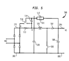
- FIGURE 5 illustrated is a schematic diagram of a boost converter 500 employing another embodiment of an energy storage circuit constructed according to the principles of the present invention.
- the boost converter 500 employs a combined energy storage circuit used to extend holdup time, an inrush current limiting circuit and a surge bypass circuit.
- the boost converter 500 employs a boost inductor 505, a boost switch 506, a boost diode 507 and an output capacitor 508 in conjunction with an energy storage circuit comprising a holdup capacitor 509, a holdup switch 510, a discrete resistor 511 and a diode 512.
- the holdup switch 510 forms a portion of an inrush limiting circuit in conjunction with a discrete resistor 513 (connected between nodes A and B along the input rail IR1), and the holdup switch 510 forms a portion of a surge bypass circuit in conjunction with a surge diode 514 which diverts at least a portion of a surge current toward the holdup capacitor 509.
- the holdup switch 510 is positioned to connect node A to node B (as with the boost converter 300) which connects the anode of the surge diode 514 to the output of the bridge rectifier as shown.
- node A node B
- node B node B
- the boost converter 300 connects the anode of the surge diode 514 to the output of the bridge rectifier as shown.
- a surge voltage occurs on the AC input line
- at least a portion of its resulting surge current will be directed through the surge diode 514 to the holdup capacitor 509 and a portion typically will be directed on through diode 512 to the output capacitor 508.
- Directing the surge current in this manner typically allows both the holdup capacitor 509 and the output capacitor 508 to participate in absorbing the surge current energy which markedly reduces any voltage which is generated by the surge current.
- Exemplary embodiments of the present invention have been illustrated above with reference to specific electronic and magnetic components. Those skilled in the art are aware, however, that components may be substituted (not necessarily with components of the same type) to create desired conditions or accomplish desired results. For instance, multiple components may be substituted for a single component and vice-versa.
Landscapes
- Engineering & Computer Science (AREA)
- Power Engineering (AREA)
- Dc-Dc Converters (AREA)
Abstract
Description
Claims (15)
- For use in a boost converter having a boost inductor coupled between an input and an output of said boost converter and an output capacitor coupled between rails of said output, an energy storage circuit for extending a holdup time of said boost converter, comprising:a holdup capacitor coupled to a first rail of said input;a holdup switch, coupled to a second rail of said input and said holdup capacitor, capable of closing during a holdup mode to allow said holdup capacitor to discharge current into said input; anda voltage stabilizing circuit, coupled between said holdup capacitor and said output capacitor, that:when said boost converter is in a normal mode, provides a substantially impeded path for charge current to flow from said output capacitor to charge said holdup capacitor, andwhen said boost converter is in an initial phase of said holdup mode, provides a substantially unimpeded path for holdup current to flow from said holdup capacitor to said output capacitor prior to said closing of said holdup switch.
- An energy storage circuit as claimed in claim 1 wherein a bridge rectifier provides DC power to said input.
- For use in a boost converter having a boost inductor coupled between an input and an output of said boost converter and an output capacitor coupled between rails of said output, a method of extending a holdup time of said boost converter, comprising the steps of:coupling a holdup capacitor to a first rail of said input;closing a holdup switch, coupled to a second rail of said input and said holdup capacitor, during a holdup mode to allow said holdup capacitor to discharge current into said input;providing a substantially impeded path for charge current to flow from said output capacitor to charge said holdup capacitor when said boost converter is in a normal mode; andproviding a substantially unimpeded path for holdup current to flow from said holdup capacitor to said output capacitor prior to said closing of said holdup switch when said boost converter is in an initial phase of said holdup mode.
- A method as claimed in claim 3 wherein said step of providing said substantially impeded path comprises the step of providing said substantially impeded path with a discrete resistor and wherein said step of providing said substantially unimpeded path comprises the step of providing said substantially unimpeded path with a diode coupled in parallel with said discrete resistor.
- A method as claimed in claim 3 wherein said holdup switch forms a portion of an inrush current limiting circuit in said boost converter, said method further comprising the step of limiting an inrush current to said boost converter.
- A method as claimed in claim 3 wherein said holdup switch forms a portion of a surge bypass circuit in said boost converter, said method further comprising the step of causing a surge to bypass said converter.
- A method as claimed in claim 6 wherein said step of causing comprises the step of diverting at least a portion of surge current toward said output capacitor.
- A method as claimed in claim 6 wherein said step of causing comprises the step of diverting at least a portion of surge current toward said holdup capacitor.
- A method as claimed in claim 3 further comprising the step of providing DC power to said input with a bridge rectifier.
- A boost converter, comprising:a bridge rectifier;a boost inductor coupled between an input and an output of said boost converter, said input receiving DC power from said bridge rectifier:an output capacitor coupled between rails of said output; andan energy storage circuit for extending a holdup time of said boost converter, comprising:a holdup capacitor coupled to a first rail of said input;a holdup switch, coupled to a second rail of said input and said holdup capacitor, capable of closing during a holdup mode to allow said holdup capacitor to discharge current into said input; anda voltage stabilizing circuit, coupled between said holdup capacitor and said output capacitor, that:when said boost converter is in a normal mode, provides a substantially impeded path for charge current to flow from said output capacitor to charge said holdup capacitor, andwhen said boost converter is in an initial phase of said holdup mode, provides a substantially unimpeded path for holdup current to flow from said holdup capacitor to said output capacitor prior to said closing of said holdup switch.
- An energy storage circuit as claimed in claim 1, or a boost converter as claimed in claim 10, wherein said voltage stabilizing circuit comprises:a discrete resistor that provides said substantially impeded path for said charge current; anda diode, coupled in parallel with said discrete resistor, that provides said substantially unimpeded path for said holdup current.
- An energy storage circuit as claimed in claim 1, or a boost converter as claimed in claim 10, wherein said holdup switch forms a portion of an inrush current limiting circuit in said boost converter.
- An energy storage circuit as claimed in claim 1. or a boost converter as claimed in claim 10, wherein said holdup switch forms a portion of a surge bypass circuit in said boost converter.
- An energy storage circuit or a boost converter as claimed in claim 13 wherein a diode in said bypass circuit diverts at least a portion of surge current toward said output capacitor.
- An energy storage circuit or a boost converter as claimed in claim 13 wherein a diode in said bypass circuit diverts at least a portion of surge current toward said holdup capacitor.
Applications Claiming Priority (2)
| Application Number | Priority Date | Filing Date | Title |
|---|---|---|---|
| US09/048,069 US6043705A (en) | 1998-03-25 | 1998-03-25 | Boost converter having extended holdup time and method of operation |
| US48069 | 1998-03-25 |
Publications (2)
| Publication Number | Publication Date |
|---|---|
| EP0945968A2 true EP0945968A2 (en) | 1999-09-29 |
| EP0945968A3 EP0945968A3 (en) | 2001-12-12 |
Family
ID=21952579
Family Applications (1)
| Application Number | Title | Priority Date | Filing Date |
|---|---|---|---|
| EP99302032A Withdrawn EP0945968A3 (en) | 1998-03-25 | 1999-03-16 | Boost converter having extended holdup time and method of operation thereof |
Country Status (3)
| Country | Link |
|---|---|
| US (1) | US6043705A (en) |
| EP (1) | EP0945968A3 (en) |
| CA (1) | CA2263896A1 (en) |
Cited By (9)
| Publication number | Priority date | Publication date | Assignee | Title |
|---|---|---|---|---|
| EP1148614A3 (en) * | 2000-04-17 | 2004-07-28 | Taiyo Yuden Co., Ltd. | Battery operated power circuit and driving method thereof |
| EP1453177A3 (en) * | 2003-02-27 | 2006-02-08 | Bosch Rexroth Aktiengesellschaft | DC/DC converter circuit |
| WO2010076734A1 (en) | 2008-12-31 | 2010-07-08 | Nxp B.V. | Switched power converter with extended hold-up time |
| CN104104225A (en) * | 2013-04-12 | 2014-10-15 | 富士电机株式会社 | Regulator circuit and integrated circuit device forming the regulator circuit |
| CN106300982A (en) * | 2015-06-05 | 2017-01-04 | 台达电子工业股份有限公司 | Power supply device with function of prolonging maintenance time |
| EP2360820B1 (en) * | 2009-12-31 | 2018-03-28 | Nxp B.V. | Surge protection circuit |
| EP3503370A1 (en) * | 2017-12-20 | 2019-06-26 | Analog Devices Global Unlimited Company | Interleaved boost converter with holdup time extension |
| EP4109712A1 (en) * | 2021-06-21 | 2022-12-28 | Infineon Technologies Austria AG | Circuit and method for extending the hold-up time |
| EP4109713A1 (en) * | 2021-06-21 | 2022-12-28 | Infineon Technologies Austria AG | Circuit and method for extending the hold-up time |
Families Citing this family (33)
| Publication number | Priority date | Publication date | Assignee | Title |
|---|---|---|---|---|
| US6694438B1 (en) * | 1999-07-02 | 2004-02-17 | Advanced Energy Industries, Inc. | System for controlling the delivery of power to DC computer components |
| US6697955B1 (en) * | 2000-07-20 | 2004-02-24 | International Business Machines Corporation | Method and apparatus for using an energy reserve to provide voltage to a power factor correction circuit in the event of a power interuption |
| US20040233690A1 (en) * | 2001-08-17 | 2004-11-25 | Ledenev Anatoli V. | Multiple power converter system using combining transformers |
| US7068016B2 (en) * | 2002-11-01 | 2006-06-27 | International Rectifier Corporation | One cycle control PFC boost converter integrated circuit with inrush current limiting, fan motor speed control and housekeeping power supply controller |
| KR100471087B1 (en) * | 2003-01-09 | 2005-03-10 | 삼성전자주식회사 | Power supply device and control method thereof |
| US7646186B2 (en) * | 2004-06-22 | 2010-01-12 | Texas Instruments Incorporated | Holdover circuit for a power converter using a bi-directional switching regulator |
| JP4396519B2 (en) * | 2004-12-28 | 2010-01-13 | カシオ計算機株式会社 | Power supply circuit and driving method of power supply circuit |
| US7760524B2 (en) * | 2007-10-17 | 2010-07-20 | Power Integrations, Inc. | Method and apparatus to reduce the volume required for bulk capacitance in a power supply |
| US8116045B2 (en) * | 2009-01-23 | 2012-02-14 | Linear Technology Corporation | Circuitry and methodology for protecting a boost DC/DC converter |
| TWI407670B (en) * | 2009-10-21 | 2013-09-01 | Delta Electronics Inc | Buck and buck/boost pfc circuit systems having auxiliary circuits and method thereof |
| US8710820B2 (en) | 2010-03-31 | 2014-04-29 | Crane Electronics, Inc. | Switched capacitor hold-up scheme for constant boost output voltage |
| FR2969418B1 (en) * | 2010-12-20 | 2012-12-14 | Schneider Toshiba Inverter | AC / DC POWER CONVERTER WITH IMPROVED POWER FACTOR AND THDI |
| BR112013021363B1 (en) | 2011-02-24 | 2020-11-03 | Crane Electronics, Inc | power converter to emit direct current voltage and method to emit the same |
| US8824167B2 (en) | 2011-07-18 | 2014-09-02 | Crane Electronics, Inc. | Self synchronizing power converter apparatus and method suitable for auxiliary bias for dynamic load applications |
| US8885308B2 (en) | 2011-07-18 | 2014-11-11 | Crane Electronics, Inc. | Input control apparatus and method with inrush current, under and over voltage handling |
| US8890630B2 (en) | 2011-07-18 | 2014-11-18 | Crane Electronics, Inc. | Oscillator apparatus and method with wide adjustable frequency range |
| US8829868B2 (en) | 2011-07-18 | 2014-09-09 | Crane Electronics, Inc. | Power converter apparatus and method with output current sensing and compensation for current limit/current share operation |
| TW201306458A (en) * | 2011-07-20 | 2013-02-01 | Compuware Technology Inc | Pseudo bypass switching system |
| US8866551B2 (en) | 2012-09-10 | 2014-10-21 | Crane Electronics, Inc. | Impedance compensation for operational amplifiers used in variable environments |
| US9143030B2 (en) * | 2012-10-09 | 2015-09-22 | Teledyne Reynolds, Inc. | Passive power factor correction incorporating AC/DC conversion |
| US9041378B1 (en) | 2014-07-17 | 2015-05-26 | Crane Electronics, Inc. | Dynamic maneuvering configuration for multiple control modes in a unified servo system |
| US9831768B2 (en) | 2014-07-17 | 2017-11-28 | Crane Electronics, Inc. | Dynamic maneuvering configuration for multiple control modes in a unified servo system |
| US9230726B1 (en) | 2015-02-20 | 2016-01-05 | Crane Electronics, Inc. | Transformer-based power converters with 3D printed microchannel heat sink |
| US9160228B1 (en) | 2015-02-26 | 2015-10-13 | Crane Electronics, Inc. | Integrated tri-state electromagnetic interference filter and line conditioning module |
| JP6288534B2 (en) * | 2015-06-11 | 2018-03-07 | 富士電機株式会社 | Power converter |
| US9293999B1 (en) | 2015-07-17 | 2016-03-22 | Crane Electronics, Inc. | Automatic enhanced self-driven synchronous rectification for power converters |
| US9780635B1 (en) | 2016-06-10 | 2017-10-03 | Crane Electronics, Inc. | Dynamic sharing average current mode control for active-reset and self-driven synchronous rectification for power converters |
| US9735566B1 (en) | 2016-12-12 | 2017-08-15 | Crane Electronics, Inc. | Proactively operational over-voltage protection circuit |
| US9742183B1 (en) | 2016-12-09 | 2017-08-22 | Crane Electronics, Inc. | Proactively operational over-voltage protection circuit |
| US9979285B1 (en) | 2017-10-17 | 2018-05-22 | Crane Electronics, Inc. | Radiation tolerant, analog latch peak current mode control for power converters |
| US10425080B1 (en) | 2018-11-06 | 2019-09-24 | Crane Electronics, Inc. | Magnetic peak current mode control for radiation tolerant active driven synchronous power converters |
| US20220271670A1 (en) * | 2019-07-29 | 2022-08-25 | Murata Manufacturing Co., Ltd. | Converter with hold-up circuit and inrush-control circuit |
| CN121308495B (en) * | 2025-12-04 | 2026-03-17 | 深圳市微源半导体股份有限公司 | Boost circuit, power chip and electronic equipment for preventing isolation tube from being damaged during power-on |
Family Cites Families (5)
| Publication number | Priority date | Publication date | Assignee | Title |
|---|---|---|---|---|
| CN1012244B (en) * | 1987-02-20 | 1991-03-27 | 株式会社东芝 | UPS |
| US5115185A (en) * | 1990-09-28 | 1992-05-19 | At&T Bell Laboratories | Single conversion power factor correction using septic converter |
| US5258901A (en) * | 1992-03-25 | 1993-11-02 | At&T Bell Laboratories | Holdover circuit for AC-to-DC converters |
| US5568041A (en) * | 1995-02-09 | 1996-10-22 | Magnetek, Inc. | Low-cost power factor correction circuit and method for electronic ballasts |
| FR2735296B1 (en) * | 1995-06-08 | 1997-08-22 | Sgs Thomson Microelectronics | CIRCUIT AND METHOD FOR CONTROLLING A CURRENT CALL LIMITER IN A POWER CONVERTER |
-
1998
- 1998-03-25 US US09/048,069 patent/US6043705A/en not_active Expired - Fee Related
-
1999
- 1999-03-02 CA CA002263896A patent/CA2263896A1/en not_active Abandoned
- 1999-03-16 EP EP99302032A patent/EP0945968A3/en not_active Withdrawn
Cited By (14)
| Publication number | Priority date | Publication date | Assignee | Title |
|---|---|---|---|---|
| EP1148614A3 (en) * | 2000-04-17 | 2004-07-28 | Taiyo Yuden Co., Ltd. | Battery operated power circuit and driving method thereof |
| EP1453177A3 (en) * | 2003-02-27 | 2006-02-08 | Bosch Rexroth Aktiengesellschaft | DC/DC converter circuit |
| WO2010076734A1 (en) | 2008-12-31 | 2010-07-08 | Nxp B.V. | Switched power converter with extended hold-up time |
| EP2360820B1 (en) * | 2009-12-31 | 2018-03-28 | Nxp B.V. | Surge protection circuit |
| CN104104225A (en) * | 2013-04-12 | 2014-10-15 | 富士电机株式会社 | Regulator circuit and integrated circuit device forming the regulator circuit |
| CN106300982B (en) * | 2015-06-05 | 2018-10-09 | 台达电子工业股份有限公司 | Power supply device with function of prolonging maintenance time |
| CN106300982A (en) * | 2015-06-05 | 2017-01-04 | 台达电子工业股份有限公司 | Power supply device with function of prolonging maintenance time |
| EP3503370A1 (en) * | 2017-12-20 | 2019-06-26 | Analog Devices Global Unlimited Company | Interleaved boost converter with holdup time extension |
| US10367411B2 (en) | 2017-12-20 | 2019-07-30 | Analog Devices Global Unlimited Company | Interleaved boost converter with holdup time extension |
| TWI702784B (en) * | 2017-12-20 | 2020-08-21 | 百慕達商亞德諾半導體環球無限公司 | Power factor correction device, system configured to provide tolerance to fault condition in an input supply, and method for operating power factor correction device |
| EP4109712A1 (en) * | 2021-06-21 | 2022-12-28 | Infineon Technologies Austria AG | Circuit and method for extending the hold-up time |
| EP4109713A1 (en) * | 2021-06-21 | 2022-12-28 | Infineon Technologies Austria AG | Circuit and method for extending the hold-up time |
| US11953971B2 (en) | 2021-06-21 | 2024-04-09 | Infineon Technologies Austria Ag | Method for extending hold-up time |
| US12143003B2 (en) | 2021-06-21 | 2024-11-12 | Infineon Technologies Austria Ag | Method for extending the hold-up time |
Also Published As
| Publication number | Publication date |
|---|---|
| EP0945968A3 (en) | 2001-12-12 |
| CA2263896A1 (en) | 1999-09-25 |
| US6043705A (en) | 2000-03-28 |
Similar Documents
| Publication | Publication Date | Title |
|---|---|---|
| US6043705A (en) | Boost converter having extended holdup time and method of operation | |
| US10680520B2 (en) | I/O protected buck then boost or boost then buck converter, with interleaving option | |
| US6404658B1 (en) | Method and apparatus for converting a DC voltage to an AC voltage | |
| US7164591B2 (en) | Bridge-less boost (BLB) power factor correction topology controlled with one cycle control | |
| EP2557650B1 (en) | Current bypass for distributed power harvesting systems using DC power sources | |
| US7061212B2 (en) | Circuit for maintaining hold-up time while reducing bulk capacitor size and improving efficiency in a power supply | |
| US5914587A (en) | Circuit for reducing switching losses of a power converter and method of operation thereof | |
| EP1484664B1 (en) | Architecture for switching power source to a load in a battery powered system | |
| CA2278250A1 (en) | High efficiency power converter | |
| US5883793A (en) | Clamp circuit for a power converter and method of operation thereof | |
| JP2020048398A (en) | Power supply conversion system with abnormal energy protection and operation method therefor | |
| US6288919B1 (en) | Single stage AC/DC converter high frequency AC distribution systems | |
| CN119482892B (en) | Gateway power circuits, circuit boards, and edge gateway devices | |
| JP5761620B2 (en) | Groundable DC / DC converter | |
| Sebastián et al. | Improving dynamic response of power factor preregulators by using two-input high-efficient post-regulators | |
| CN113497555B (en) | Switching converter and method | |
| CN220492696U (en) | Power-down holding circuit and power supply device | |
| US12444924B2 (en) | DC-DC converter | |
| KR101343953B1 (en) | Double conversion uninterruptible power supply of eliminated battery discharger | |
| US20250260314A1 (en) | Electronic device including a power factor correction circuit and method for controlling the power factor correction circuit | |
| CN118829038B (en) | A circuit for reducing standby power consumption of a PFC circuit | |
| KR102838906B1 (en) | High voltage fast switching apparatus for stabilizing a voltage of hydrogen fuel cell and its control method | |
| CN121193093A (en) | Multi-stage boost power converter circuit with low energy consumption | |
| CN117013498A (en) | A power-down holding circuit and power supply device | |
| KR101356385B1 (en) | Power converting apparatus and control method for power converter |
Legal Events
| Date | Code | Title | Description |
|---|---|---|---|
| PUAI | Public reference made under article 153(3) epc to a published international application that has entered the european phase |
Free format text: ORIGINAL CODE: 0009012 |
|
| AK | Designated contracting states |
Kind code of ref document: A2 Designated state(s): AT BE CH CY DE DK ES FI FR GB GR IE IT LI LU MC NL PT SE |
|
| AX | Request for extension of the european patent |
Free format text: AL;LT;LV;MK;RO;SI |
|
| PUAL | Search report despatched |
Free format text: ORIGINAL CODE: 0009013 |
|
| AK | Designated contracting states |
Kind code of ref document: A3 Designated state(s): AT BE CH CY DE DK ES FI FR GB GR IE IT LI LU MC NL PT SE |
|
| AX | Request for extension of the european patent |
Free format text: AL;LT;LV;MK;RO;SI |
|
| RIC1 | Information provided on ipc code assigned before grant |
Free format text: 7H 02M 3/158 A, 7H 02J 9/06 B, 7H 02H 9/00 B |
|
| AKX | Designation fees paid | ||
| REG | Reference to a national code |
Ref country code: DE Ref legal event code: 8566 |
|
| STAA | Information on the status of an ep patent application or granted ep patent |
Free format text: STATUS: THE APPLICATION IS DEEMED TO BE WITHDRAWN |
|
| 18D | Application deemed to be withdrawn |
Effective date: 20020613 |