EP0946884B1 - Simulateur de controle d'un radar anticollisions - Google Patents
Simulateur de controle d'un radar anticollisions Download PDFInfo
- Publication number
- EP0946884B1 EP0946884B1 EP97954541A EP97954541A EP0946884B1 EP 0946884 B1 EP0946884 B1 EP 0946884B1 EP 97954541 A EP97954541 A EP 97954541A EP 97954541 A EP97954541 A EP 97954541A EP 0946884 B1 EP0946884 B1 EP 0946884B1
- Authority
- EP
- European Patent Office
- Prior art keywords
- signal
- output
- input
- radar system
- collision avoidance
- Prior art date
- Legal status (The legal status is an assumption and is not a legal conclusion. Google has not performed a legal analysis and makes no representation as to the accuracy of the status listed.)
- Expired - Lifetime
Links
- 238000012360 testing method Methods 0.000 title claims abstract description 22
- 230000003247 decreasing effect Effects 0.000 claims abstract description 9
- 230000007423 decrease Effects 0.000 claims description 5
- 238000000034 method Methods 0.000 claims description 3
- 239000003990 capacitor Substances 0.000 claims description 2
- 230000008878 coupling Effects 0.000 claims 1
- 238000010168 coupling process Methods 0.000 claims 1
- 238000005859 coupling reaction Methods 0.000 claims 1
- 238000010998 test method Methods 0.000 claims 1
- 230000001419 dependent effect Effects 0.000 description 3
- 239000002184 metal Substances 0.000 description 3
- 238000010408 sweeping Methods 0.000 description 3
- 230000007704 transition Effects 0.000 description 3
- 238000001514 detection method Methods 0.000 description 2
- 238000004364 calculation method Methods 0.000 description 1
- 230000006870 function Effects 0.000 description 1
- 238000005259 measurement Methods 0.000 description 1
- 238000012986 modification Methods 0.000 description 1
- 230000004048 modification Effects 0.000 description 1
- 238000012545 processing Methods 0.000 description 1
- 238000004088 simulation Methods 0.000 description 1
Images


Classifications
-
- G—PHYSICS
- G01—MEASURING; TESTING
- G01S—RADIO DIRECTION-FINDING; RADIO NAVIGATION; DETERMINING DISTANCE OR VELOCITY BY USE OF RADIO WAVES; LOCATING OR PRESENCE-DETECTING BY USE OF THE REFLECTION OR RERADIATION OF RADIO WAVES; ANALOGOUS ARRANGEMENTS USING OTHER WAVES
- G01S7/00—Details of systems according to groups G01S13/00, G01S15/00, G01S17/00
- G01S7/02—Details of systems according to groups G01S13/00, G01S15/00, G01S17/00 of systems according to group G01S13/00
- G01S7/40—Means for monitoring or calibrating
- G01S7/4052—Means for monitoring or calibrating by simulation of echoes
-
- G—PHYSICS
- G01—MEASURING; TESTING
- G01S—RADIO DIRECTION-FINDING; RADIO NAVIGATION; DETERMINING DISTANCE OR VELOCITY BY USE OF RADIO WAVES; LOCATING OR PRESENCE-DETECTING BY USE OF THE REFLECTION OR RERADIATION OF RADIO WAVES; ANALOGOUS ARRANGEMENTS USING OTHER WAVES
- G01S13/00—Systems using the reflection or reradiation of radio waves, e.g. radar systems; Analogous systems using reflection or reradiation of waves whose nature or wavelength is irrelevant or unspecified
- G01S13/88—Radar or analogous systems specially adapted for specific applications
- G01S13/93—Radar or analogous systems specially adapted for specific applications for anti-collision purposes
- G01S13/931—Radar or analogous systems specially adapted for specific applications for anti-collision purposes of land vehicles
- G01S2013/9327—Sensor installation details
- G01S2013/93271—Sensor installation details in the front of the vehicles
-
- G—PHYSICS
- G01—MEASURING; TESTING
- G01S—RADIO DIRECTION-FINDING; RADIO NAVIGATION; DETERMINING DISTANCE OR VELOCITY BY USE OF RADIO WAVES; LOCATING OR PRESENCE-DETECTING BY USE OF THE REFLECTION OR RERADIATION OF RADIO WAVES; ANALOGOUS ARRANGEMENTS USING OTHER WAVES
- G01S7/00—Details of systems according to groups G01S13/00, G01S15/00, G01S17/00
- G01S7/02—Details of systems according to groups G01S13/00, G01S15/00, G01S17/00 of systems according to group G01S13/00
- G01S7/40—Means for monitoring or calibrating
- G01S7/4052—Means for monitoring or calibrating by simulation of echoes
- G01S7/4056—Means for monitoring or calibrating by simulation of echoes specially adapted to FMCW
-
- G—PHYSICS
- G01—MEASURING; TESTING
- G01S—RADIO DIRECTION-FINDING; RADIO NAVIGATION; DETERMINING DISTANCE OR VELOCITY BY USE OF RADIO WAVES; LOCATING OR PRESENCE-DETECTING BY USE OF THE REFLECTION OR RERADIATION OF RADIO WAVES; ANALOGOUS ARRANGEMENTS USING OTHER WAVES
- G01S7/00—Details of systems according to groups G01S13/00, G01S15/00, G01S17/00
- G01S7/02—Details of systems according to groups G01S13/00, G01S15/00, G01S17/00 of systems according to group G01S13/00
- G01S7/40—Means for monitoring or calibrating
- G01S7/4052—Means for monitoring or calibrating by simulation of echoes
- G01S7/4082—Means for monitoring or calibrating by simulation of echoes using externally generated reference signals, e.g. via remote reflector or transponder
Definitions
- the present invention relates to a method of and a simulator for testing the performance accuracy or calibrating a collision avoidance radar system.
- the collision avoidance radar system 10 shown in Fig. 1 is typically installed in an automobile with the antenna 106 in the front or grill area of the automobile.
- the system operates by transmitting a signal from the antenna 106 and determining from a signal received back the distance (D) the antenna 106 is from simulator 108 or other reflecting object, such as another automobile. From the received signal, the radar system 10 can also determine the rate (dD/dt) the object or other vehicle is moving. By processing the received signal, an alarm or other device can be activated to enable the vehicle operator to avoid a collision with the object or vehicle.
- the system shown in Fig. 1 includes a oscillator 100 configured to sweep over a range of frequencies.
- the output of oscillator 100 is provided to a splitter 102.
- a first output of splitter 102 is provided as a local oscillator signal (F LO ) to the first input of a mixer 110.
- a second output of the splitter 102 is provided to isolator 104.
- the isolator 104 provides the signal from the splitter 102 to the input of the antenna 106 to be transmitted, and provides the signal received from the antenna 106 as an RF signal (F RF ) to a second input of mixer 110.
- F RF RF signal
- the oscillator 100 typically sweeps through a range of frequencies having a minimum of 76 GHz and a maximum of 77 GHz.
- the 76-77 GHz range is assigned by the Federal Communications Commission (FCC) for collision avoidance radar systems.
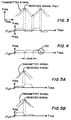
- the oscillator 100 typically sweeps through a 250 MHz range of frequencies within the 76-77 GHz limits in a 1.2 msec time period as illustrated in Fig. 2. In Fig. 2, the sweep range is centered at 76.5 GHz, but the 250 MHz range may also be found centered closer to one of the 76 GHz or 77 GHz limits.
- the signal provided from the oscillator 100 is provided through the isolator 104 and antenna 106 as a transmitted signal which is illustrated in Fig. 3.
- a reflected signal is then received by the antenna 106 and provided by the isolator 104 as the F RF signal, also as illustrated in Fig. 3.
- the received signal is shown in Fig. 3 shifted in frequency from the transmitted signal and will be shifted in frequency dependent on the distance D, shown in Fig. 1.
- the distance D is a distance which a reflecting object such as the 1 2 meter standard 108 is located from the antenna 104. If the distance D is zero, no frequency shift will occur between the transmitted and received signals.
- Fig. 3 also shows an intermediate frequency signal F IF which is the difference in the transmitted signal F LO and the received signal F RF provided at the inputs of mixer 110. Because the mixer 110 cannot distinguish between positive and negative, the actual signal provided from mixer 100 F IF is a positive frequency signal changing with time as illustrated in Fig. 4.
- the frequency of the signal F IF output from mixer 110 is converted to a corresponding voltage by a discriminator, or frequency to voltage converter 112. Since transitions such as 120 occur at regular 1.2 msec intervals, as shown in Fig. 4, the transitions 120 can be filtered out by the discriminator 112. The voltage output from discriminator 112 can then be processed to determine the distance D.
- the rate an object is moving toward or away from the antenna 106, or the change in D with respect to time (dD/dt) can also be determined by the circuitry of Fig. 1.
- the object such as simulator 108
- moving farther away from the antenna 106 the received signal will increase in frequency relative to the transmitted signal as shown in Fig. 5A.
- frequency F IF provided from mixer 110 during a period ⁇ t when the transmitted signal is increasing in frequency will be smaller than during a period ⁇ t when the transmitted signal is decreasing in frequency, dependent on dD/dt, as illustrated in Fig. 5A.
- the received signal will decrease in frequency relative to the transmitted signal as shown in Fig. 5B.
- frequency F IF provided from mixer 110 during a period when the transmitted signal is increasing in frequency will then be larger than during a period when the transmitted signal is decreasing in frequency, dependent on dD/dt, as further illustrated in Fig. 5B.
- dD/dt can, thus, be determined.
- the device To assure proper performance of the collision avoidance radar of Fig. 1, the device must be regularly tested or calibrated. During calibration, assurances must be made that the oscillator 100 is operating inside the 76-77 GHz range specified by the FCC, even though the radar may be functioning properly outside that range. Further, the 250 MHz sweep range ⁇ f and 1.2 msec sweep period ⁇ t must be verified to assure accurate distance calculations are being made using equation (4). A receiver is typically connected to the oscillator 100 during calibration to assure the oscillator is functioning properly.
- Calibration is also performed using the simulator 108 to check that the radar indicates proper distances D accurately up to 100 meters.
- the simulator 108 is also utilized to assure the radar system indicates proper change in distance measurements dD/dt as described above.
- the present invention enables testing a collision avoidance radar system while using significantly less space than a 1 2 meter metal plate standard requires. Further, dD/dt tests can be made without requiring the awkward movement of equipment as is required with a 1 2 meter plate simulator.
- the present invention also enables testing the frequency sweep range ⁇ f and time period ⁇ of a signal provided from oscillator 100 without requiring that additional test equipment be connected to the oscillator.
- EP-A-0182418 describes a simulator for testing a radar system by generating a signal with a delay line offset in frequency from a signal received from the radar system under test and transmitting the offset frequency signal to the radar system under test.
- the present invention provides, as is known from EP-A-0182418, a method for testing a collision avoidance radar system comprising:
- the step of a signal offset in frequency comprises generating a first portion of the offset signal having a first difference in frequency from the signal received from the collision avoidance radar system when the signal from the collision avoidance radar system is increasing in frequency; and generating a second portion of the offset signal having a second difference in frequency from the signal received from the collision avoidance radar system when the signal from the collision avoidance radar system is decreasing in frequency, the first difference in frequency and the second difference in frequency being controlled so that the collision avoidance radar system should indicate an object is moving at a rate (dD/dt) upon receiving the offset signal.
- the present invention provides, as is known from EP-A-0182418 a simulator for testing a collision avoidance radar system, the simulator comprising:
- the simulator further comprises: an isolator connected to the antenna for providing the received signal from the antenna to the first input of the first mixer and for providing the output of the second mixer as the transmitted signal to the antenna; a voltage controlled oscillator having an output connected to the second input of the first mixer and the second input of the second mixer, and having a voltage control input; a phase detector having an input coupled to the output of the first mixer, the phase detector comparing a signal from the output of the first mixer with a reference signal, the phase detector having an output providing a signal to the voltage control input of the VCO to enable the VCO output to provide a signal having a frequency equal to the signal provided from the collision avoidance radar system offset by the reference signal frequency; a numerically controlled oscillator having an output connected to a first input of the second mixer and an input, the NCO providing a signal at its output equal to the reference signal frequency offset by an amount as controlled by a numerical value provided at the input of the NCO so that the collision
- the provision of the differential controlled offset according to whether the radar system output is increasing or decreasing in frequency can cause the output of the first mixer to appear as shown in Figs. 5A and 5B.
- the simulator may further include components to indicate the frequency range and amplitude of the radar system output as determined from the tracking signal which it generates.
- Fig. 6 shows a simulator of the present invention utilized to test or calibrate a collision avoidance radar system 10 as shown in Fig. 1.
- the simulator includes an antenna 606 which in operation is placed immediately next to the antenna 106 of the collision avoidance radar system 10.
- the antenna 606 is connected to an isolator 608 which provides a received signal (F) received from the radar system 10 to a first input of mixer 610.
- the isolator 608 is also connected to the output of a mixer 612 to provide a signal from mixer 612 as a transmitted signal through antenna 606 to the radar system 10.
- An attenuator 613 is connected between mixer 612 and isolator 608 so that a signal transmitted from the antenna 606 will simulate the signal strength of a similar signal reflected from an object at a distance D.
- a tracking signal F T is provided to a second input of mixer 610 and mixer 612 by a voltage controlled oscillator (VCO) 614.
- VCO voltage controlled oscillator
- the tracking signal F T is controlled to track the received signal F with a frequency offset by a reference signal Fo.
- the reference signal Fo in Fig. 6 is assumed to be 10 MHz, although other values may be chosen.
- the output of mixer 610 will be a signal having the reference frequency Fo along with broadband noise.
- the output of the mixer 610 is provided through a preamplifier 616 to a low pass filter 618.
- the low pass filter 618 functions to limit broadband noise in a signal applied to amplifier 620 so that the signal to noise ratio for the amplifier 620 is within acceptable limits.
- the amplifier 620 provides a relative signal strength signal (V RSS ) test connection enabling an amplitude of the signal F from the collision avoidance radar system to be determined.
- the amplifier 620 further provides a square wave output with a fixed amplitude to bandpass filter 622.
- the bandpass filter 622 provides a fixed amplitude sine wave output having a bandpass range centered on the reference signal Fo, here 10 MHz.
- a phase detector 624 receives the output of bandpass filter 622.
- the phase detector 624 compares the signal from filter 622 with the reference signal Fo and provides an output indicating any difference to the voltage control input of VCO 614.
- the phase detector 624 which is preferred, has components illustrated in Fig. 6 which are found in a Wiltron 360 Analyzer manufactured by Wiltron Company, Morgan Hill, CA.
- the phase detector 624 is a quadrature phase detector as configured in the Wiltron 360 Analyzer because the signal F T could be F ⁇ Fo, and the circuitry of the phase detector 624 enables detection of a desired one of the signals, preferably F+Fo, so that the tracking signal F T can be used to accurately measure the frequency of the collision avoidance radar signal F.
- the signal F T could be either 76.51 GHz or 76.49 GHz.
- the phase detector 624 configured as shown would enable detection of only the 76.51 GHz signal.
- the phase detector 624 includes an oscillator 626 and two D-type flip-flops 628 and 630.
- the oscillator 626 provides a signal four times the reference signal frequency, here 40 MHz, to the clock inputs of flip-flops 628 and 630.
- the Q output of flip-flop 628 is connected to the D input of flip-flop 630.
- the Q output of flip-flop 630 is connected to the D input of flip-flop 628.
- the Q outputs of the flip-flops 628 and 630 each provide the 10 MHz signal Fo, the Q output of flip-flop 628 being 90 degrees out of phase with the Q output of flip-flop 630.
- the Q output of flip-flop 628 is provided to a first input of multiplier 634 and the Q output of flip-flop 630 is provided to a first input of multiplier 632.
- Second inputs of multipliers 632 and 634 are provided from filter 622.
- the output of multiplier 634 is provided to a lock signal generator 636.
- the lock signal generator 636 provides an unlock signal when the signal provided from multiplier 634 from bandpass filter 622 is absent or is F-F T , and a lock signal when the signal provided to multiplier 634 by bandpass filter 622 is F T -F.
- the lock signal generator output is provided to a search signal generator 638, as well as to integrators 640 and 642 connected in series to the output of multiplier 632.
- the search signal generator 638 provides an output through summer 644 to the input of oscillator 614.
- the search signal generator 638 provides a continuously sweeping signal to sweep a frequency at the VCO 614 output through the range of possible frequencies for F when the lock signal generator 636 indicates an unlocked condition.
- the search signal generator 638 has its output signal disabled when the lock signal generator indicates a locked condition when the signal F T is tracking the signal F with an offset of Fo.
- the series integrators 640 and 642 likewise provide a signal through summer 644 to the input of VCO 614.
- the integrators 640 and 642 each include a switch connected in parallel with a capacitor. The switch is controlled by the output of the lock signal generator to be closed in an unlocked condition and opened in a locked condition.
- integrators 640 and 642 are disabled and the output of multiplier 632 is provided to summer 644 with a low gain and a finite phase error.
- integrators 640 and 642 are enabled and provide a signal from multiplier 632 with a zero phase error and high gain through summer 644 to control the VCO 614 input so that the signal F T tracks the signal F with an offset Fo.
- the lock signal generator 636 will initially be in an unlocked state.
- the search signal generator 638 will then provide a sweeping voltage to summer 644 causing the signal F T from VCO 614 to sweep through frequencies of approximately 76-77 GHz.
- the lock signal generator will disable integrators 640 and 642 so the multiplier 632 will provide a low gain signal path to VCO 614 which will momentarily phase lock VCO 614 if the search signal generator 638 causes VCO 614 to sweep through F ⁇ Fo. If the signal F T is not equal to F ⁇ Fo, the DC signal provided from multiplier 634 to lock signal generator 636 will be 0 volts.
- the voltage control input to VCO 614 is provided as a test connection to provide the signal V FT .
- the signal V FT enables determination of the frequency of F when phase lock is obtained without requiring a connection to the oscillator 100 of the collision avoidance radar system 10 shown in Fig. 1 as in previous test configurations.
- a second input of mixer 612 is connected to the output of a numerically controlled oscillator (NCO) 646.
- NCO numerically controlled oscillator
- a typical 32 bit NCO is the Analog Devices AD9850.
- a configuration for a 4 bit NCO 646 is shown in Fig. 7, although a 32 bit NCO is preferably utilized.
- the NCO of Fig. 7 includes a series of D flip-flops 700 with Q outputs connected to a first set of inputs A 0-3 of an adder 702. Outputs ⁇ 0-3 of the adder 702 are then fed back to the D inputs of the flip-flops 700.
- a second set of inputs B 0-3 to the adder are provided as an input (INPUT) to the NCO.
- the Q outputs of flip-flops 700 are further provided through a sine output read only memory (SINE ROM) 704 and D/A converter 706 to provide the output of the NCO (F NCO .)
- a count provided by adder 702 will proceed with the clock (CK) provided to flip-flops 700 and proceed in increments depending on the B 0-3 input to the adder 702. For instance, if the B 0-3 input is 0001, the count will proceed by binary 1's, or if the B 0-3 input is 0010, the count will proceed by binary 2's.
- the SINE ROM 704 output will then increase in value until overflow of the adder 702 and then reset creating a signal at the output (SINE OUTPUT) of the D/A converter 706 having a frequency controlled by the B 0-3 input.
- An input (INPUT) to the NCO 646 in Fig. 6 is provided from registers 648 and 650.
- the values N A and N B stored in registers 648 and 650 and an appropriate CK provided to the NCO 646 enables the NCO 646 to provide a signal F NCO having the frequency of the reference signal Fo offset by an amount ⁇ F as controlled by registers 648 and 650.
- the output of mixer 612 will be F T ⁇ F NCO .
- the signal FT + F NCO will be above the range of frequencies accepted by the collision avoidance radar 10 and will be filtered out as long as Fo is selected as a high enough value, such as the 10 MHz signal suggested.
- F T being F+Fo
- F NCO Fo- ⁇ F
- the values stored in registers 648 and 650 are provided by a processor and controlled so that offset ⁇ F will cause the collision avoidance radar system 10 to indicate an object is located a chosen distance D away.
- Two separate registers 648 and 650 are utilized to enable the offset ⁇ F to be controlled to cause the collision avoidance radar system 10 to indicate an object is moving at a rate dD/dt.
- the circuit of Fig. 6 includes a differentiator 652, comparator 654 and inverter 656.
- the differentiator 652 has an input connected to integrator 642. With the integrator 642 providing a signal 800 as shown in Fig. 8 when phase lock occurs, the output of the differentiator 652 will be the signal 802. Because the signal 800 increases and decreases voltage in correspondence with any increase or decrease in the frequency of F, the state of signal 802 will indicate whether F is increasing or decreasing in frequency. To provide a voltage swing to adequately drive subsequent circuitry, the output of differentiator 652 is provided through a comparator 654. The output of comparator 654 will, thus, transition between ground or a logic 0 and a logic 1 depending on whether the signal F is increasing or decreasing in frequency.
- the output of comparator 654 is provided to an enable input of register 650.
- the output of comparator 654 is further provided through an inverter 656 to an enable input of register 648.
- F when F is increasing in frequency the output of one of registers 648 and 650 will be enabled, and when F is decreasing in frequency the output of the other one of registers 648 and 650 will be enabled.
- N A and N B the signal transmitted from antenna 606 will make the output of the mixer 110 in the collision avoidance radar system 10 of Fig. 1 to appear as shown in Fig. 5.
- the values N A and N B stored in registers 648 and 650 are controlled so that the offset ⁇ F will cause the collision avoidance radar system to indicate an object is moving at a chosen rate (dD/dt).
Landscapes
- Engineering & Computer Science (AREA)
- Computer Networks & Wireless Communication (AREA)
- Physics & Mathematics (AREA)
- General Physics & Mathematics (AREA)
- Radar, Positioning & Navigation (AREA)
- Remote Sensing (AREA)
- Radar Systems Or Details Thereof (AREA)
Claims (8)
- Procédé de test d'un système radar anticollision (10) comprenant :caractérisé en ce que l'étape de génération d'un signal décalé en fréquence comprend :la réception d'un signal (F, FRF) depuis le système radar anticollision (10) ;la génération d'un signal (FT) décalé en fréquence par rapport au signal reçu du système radar anticollision, le décalage en fréquence étant commandé de telle sorte que le système radar anticollision devrait indiquer qu'un objet est situé à une distance (D) lors de la réception du signal décalé ; etla transmission du signal décalé au système radar anticollision,la génération d'une première partie du signal décalé présentant une première différence de fréquence par rapport au signal reçu du système radar anticollision lorsque le signal provenant du système radar anticollision augmente en fréquence; etla génération d'une seconde partie du signal décalé présentant une seconde différence de fréquence par rapport au signal reçu depuis le système radar anticollision lorsque le signal provenant du système radar anticollision diminue en fréquence, la première différence de fréquence et la seconde différence de fréquence étant commandées de telle sorte que le système radar anticollision devrait indiquer qu'un objet se déplace à une vitesse (dD/dt) à la réception du signal décalé.
- Procédé selon la revendication 1 et comprenant en outre l'étape consistant à :indiquer la plage de fréquences du signal provenant du système radar anticollision telle qu'elle est déterminée d'après le signal décalé.
- Simulateur destiné à tester un système radar anticollision selon la revendication 1, le simulateur comprenant :une antenne (606) destinée à fournir un signal reçu depuis le système radar anticollision et à fournir un signal émis au système radar anticollision ;un premier mélangeur (610) comportant une première entrée, une seconde entrée et une sortie etun second mélangeur (612) comportant une première entrée, une seconde entrée et une sortie ;un isolateur (608) relié à l'antenne afin de fournir le signal reçu depuis l'antenne à la première entrée du premier mélangeur et à fournir la sortie du second mélangeur en tant que signal émis vers l'antenne ;un oscillateur commandé en tension (VCO) (614) comportant une sortie reliée à une seconde entrée du premier mélangeur et à la seconde entrée du second mélangeur, et comportant une entrée de tension de commande ;un détecteur de phase (624) comportant une entrée reliée à la sortie du premier mélangeur, le détecteur de phase comparant un signal provenant de la sortie du premier mélangeur à un signal de référence, le détecteur de phase ayant une sortie fournissant un signal à l'entrée de tension de commande de l'oscillateur VCO pour permettre que la sortie de l'oscillateur VCO fournisse un signal présentant une fréquence égale au signal fourni à partir du système radar anticollision décalé par la fréquence du signal de référence ;un oscillateur commandé numériquement (NCO) (646) ayant une sortie reliée à une première entrée du second mélangeur et une entrée, l'oscillateur NCO fournissant un signal à sa sortie égal à la fréquence du signal de référence décalée d'une valeur qui est commandée par une valeur numérique fournie à l'entrée de l'oscillateur NCO de telle sorte que le système radar anticollision devrait indiquer qu'un objet est situé à une distance (D) lors de la réception du signal émis ;un différentiateur (652) comportant une entrée reliée au détecteur de phase et une sortie ; etun moyen de mémorisation (648, 650, 654, 656) recevant la sortie du différentiateur et fournissant une première valeur numérique à l'entrée de l'oscillateur NCO lorsque l'état de la sortie du différentiateur indique que la sortie de l'oscillateur VCO devrait augmenter la fréquence et fournir une seconde valeur numérique à l'entrée de l'oscillateur NCO lorsque l'état de la sortie du différentiateur indique que la sortie de l'oscillateur VCO devrait diminuer la fréquence, de sorte que le système radar anticollision devrait indiquer qu'un objet se déplace à une vitesse (dD/dt) lors de la réception du signal émis.
- Simulateur selon la revendication 3, dans lequel le moyen de mémorisation comprend :un comparateur (654) ayant une première entrée reliée à la sortie du différentiateur, une seconde entrée reliée à une référence de tension et une sortie ;un inverseur (656) ayant une entrée reliée à la sortie du comparateur et une sortie ;un premier registre (648) destiné à mémoriser une valeur, le premier registre ayant une sortie reliée à l'entrée de l'oscillateur NCO et ayant une entrée de validation reliée à la sortie de l'inverseur ; etun second registre (650) destiné à mémoriser une valeur, le second registre ayant une sortie reliée à l'entrée de l'oscillateur NCO et ayant une entrée de validation reliée à l'entrée de l'inverseur.
- Simulateur selon la revendication 3 ou 4 et comprenant en outre :une connexion de test (VFT) reliée à la sortie du détecteur de phase, la connexion de test indiquant la plage de fréquences du signal reçu depuis le système radar anticollision telle qu'elle est déterminée d'après un signal à la sortie du détecteur de phase.
- Simulateur selon l'une quelconque des revendications 3 à 5, dans lequel le détecteur de phase est un détecteur de phase en quadrature comprenant :un premier multiplicateur (634) ayant une première entrée reliée à la sortie du premier mélangeur, une seconde entrée et une sortie ;un second multiplicateur (632) ayant une première entrée reliée à la sortie du premier mélangeur, une seconde entrée et une sortie ;un générateur de signal de référence (626, 628, 630) destiné à fournir un signal de référence à la seconde entrée du premier multiplicateur et à la seconde entrée du second multiplicateur, le signal de référence appliqué au premier multiplicateur étant déphasé de 90 degrés par rapport au signal de référence tel qu'il est appliqué au second multiplicateur ;un générateur de signal de verrouillage (636) relié à la sortie du premier multiplicateur, le générateur de signal de verrouillage fournissant un premier signal lorsque la sortie du premier multiplicateur fournit principalement un signal en courant continu d'une première valeur de tension, et un second signal lorsque la sortie du premier multiplicateur indique que la sortie fournit principalement un signal en courant continu d'une seconde valeur de tension ;un générateur de signal de recherche (638) ayant une entrée reliée à la sortie du générateur de signal de verrouillage et une sortie reliée par l'intermédiaire d'un sommateur à l'entrée de l'oscillateur VCO, le générateur de signal de recherche, lorsqu'il reçoit le premier signal du générateur de signal de verrouillage, fournissant une tension variable à l'entrée de l'oscillateur VCO pour faire balayer une fréquence à la sortie de l'oscillateur VCO sur la plage de fréquences qui peuvent être fournies par le signal provenant du système radar anticollision, le générateur de signal de recherche, lorsqu'il reçoit le second signal du générateur de signal de verrouillage, désactivant sa sortie ; etau moins un intégrateur (640, 642) comprenant un commutateur relié en parallèle à un condensateur en vue de relier la sortie du second multiplicateur par l'intermédiaire du sommateur à l'entrée de l'oscillateur VCO, le commutateur étant relié au générateur de signal de verrouillage de façon à ce que le commutateur soit commandé pour se fermer lorsque le générateur de signal de verrouillage fournit le premier signal et pour s'ouvrir lorsque le générateur de signal de verrouillage fournit le second signal.
- Simulateur selon la revendication 6, dans lequel la première valeur de tension provenant du premier multiplicateur est nulle ou bien une valeur positive et la seconde valeur de tension provenant du premier multiplicateur est une valeur négative.
- Simulateur selon la revendication 6 ou 7, dans lequel le détecteur de phase en quadrature comprend en outre :un différentiateur (652) ayant une entrée reliée à la sortie dudit au moins un intégrateur (640, 642) et une sortie ;un comparateur (654) ayant une première entrée reliée à la sortie du différentiateur, une seconde entrée reliée à une référence de tension et une sortie ;un inverseur (656) ayant une entrée reliée à la sortie du comparateur et une sortie ;un premier registre (648) destiné à mémoriser une valeur, le premier registre ayant une sortie reliée à l'entrée de l'oscillateur NCO et ayant une entrée de validation reliée à la sortie de l'inverseur ; etun second registre (650) destiné à mémoriser une valeur, le second registre ayant une sortie reliée à l'entrée de l'oscillateur NCO et ayant une entrée de validation reliée à l'entrée de l'inverseur.
Applications Claiming Priority (3)
| Application Number | Priority Date | Filing Date | Title |
|---|---|---|---|
| US771051 | 1996-12-20 | ||
| US08/771,051 US5821897A (en) | 1996-12-20 | 1996-12-20 | Simulator for testing a collision avoidance radar system |
| PCT/US1997/022447 WO1998028633A1 (fr) | 1996-12-20 | 1997-12-09 | Simulateur de controle d'un radar anticollisions |
Publications (2)
| Publication Number | Publication Date |
|---|---|
| EP0946884A1 EP0946884A1 (fr) | 1999-10-06 |
| EP0946884B1 true EP0946884B1 (fr) | 2003-03-26 |
Family
ID=25090543
Family Applications (1)
| Application Number | Title | Priority Date | Filing Date |
|---|---|---|---|
| EP97954541A Expired - Lifetime EP0946884B1 (fr) | 1996-12-20 | 1997-12-09 | Simulateur de controle d'un radar anticollisions |
Country Status (6)
| Country | Link |
|---|---|
| US (1) | US5821897A (fr) |
| EP (1) | EP0946884B1 (fr) |
| JP (1) | JP3996645B2 (fr) |
| AT (1) | ATE235694T1 (fr) |
| DE (1) | DE69720258T2 (fr) |
| WO (1) | WO1998028633A1 (fr) |
Families Citing this family (14)
| Publication number | Priority date | Publication date | Assignee | Title |
|---|---|---|---|---|
| US5920281A (en) * | 1997-08-05 | 1999-07-06 | Wiltron Company | Radar test system for collision avoidance automotive radar |
| SE511151C2 (sv) * | 1997-10-21 | 1999-08-09 | Celsiustech Electronics Ab | Förfarande och anordning för att kontrollera funktionen hos en bilradar av FMCW-typ |
| DE19946161A1 (de) * | 1999-09-27 | 2001-04-26 | Siemens Ag | Verfahren zur Abstandsmessung |
| KR20050007372A (ko) | 2002-05-03 | 2005-01-17 | 디에스엠 아이피 어셋츠 비.브이. | 방사선 경화성 수지 조성물 및 이를 이용한 쾌속 성형법 |
| US20040254728A1 (en) * | 2002-10-25 | 2004-12-16 | Poropat George Vladimir | Collision warning system and method |
| DE102004062496A1 (de) * | 2004-12-24 | 2006-07-06 | Daimlerchrysler Ag | Verfahren zum Betreiben eines Kollisionsvermeidungs- oder Kollisionsfolgenminderungssystems eines Fahrzeugs sowie Kollisionsvermeidungs- oder Kollisionsfolgenminderungssystem |
| US20070120970A1 (en) * | 2005-11-15 | 2007-05-31 | Goffin Glen P | Video telephony device having automatic user detection and recognition capabilities to provide user-specific information |
| US7295151B2 (en) * | 2005-12-19 | 2007-11-13 | Honeywell International Inc. | Systems and methods for self-test of a radar altimeter |
| RU2449308C1 (ru) * | 2010-09-29 | 2012-04-27 | Федеральное государственное автономное образовательное учреждение высшего профессионального образования "ЮЖНЫЙ ФЕДЕРАЛЬНЫЙ УНИВЕРСИТЕТ" | Имитатор движущихся объектов |
| FR3027161B1 (fr) * | 2014-10-09 | 2017-05-12 | Centre Nat Rech Scient | Procede de generation de rayonnements electromagnetiques haute puissance |
| EP3495363B1 (fr) * | 2016-07-28 | 2023-08-23 | Shionogi & Co., Ltd | Composés cycliques condensés contenant de l'azote ayant un effet antagoniste du récepteur de la dopamine d3 |
| RU186130U1 (ru) * | 2018-06-04 | 2019-01-10 | Федеральное государственное автономное образовательное учреждение высшего образования "Уральский федеральный университет имени первого Президента России Б.Н. Ельцина" | Многофункциональный имитатор радиолокационных целей |
| RU2707506C1 (ru) * | 2019-06-10 | 2019-11-27 | Акционерное общество "НИИ измерительных приборов - Новосибирский завод имени Коминтерна" (АО "НПО НИИИП-НЗиК") | Способ контроля работоспособности радиолокационной станции и комплекс для его осуществления |
| CN116990819B (zh) * | 2023-09-27 | 2023-12-15 | 成都国营锦江机器厂 | 一种防撞雷达起动检测保护方法、系统及装置 |
Family Cites Families (20)
| Publication number | Priority date | Publication date | Assignee | Title |
|---|---|---|---|---|
| US3745579A (en) * | 1969-02-26 | 1973-07-10 | Us Navy | Double mixing doppler simulator |
| US3832712A (en) * | 1973-02-15 | 1974-08-27 | Singer Co | Doppler signal simulator |
| US3860925A (en) * | 1974-01-09 | 1975-01-14 | Singer Co | Velocity-altimeter frequency-modulation continuous-wave doppler system |
| US3924341A (en) * | 1974-06-17 | 1975-12-09 | Itt | Doppler microwave landing system signal simulator |
| US4209786A (en) * | 1979-01-15 | 1980-06-24 | The United States Of America As Represented By The Secretary Of The Army | Near carrier AM-FM calibration technique |
| US4477811A (en) * | 1979-07-02 | 1984-10-16 | California Microwave, Inc. | Automatic MDS level analyzer |
| US4435712A (en) * | 1981-08-13 | 1984-03-06 | Rca Corporation | FM-CW Radar ranging system with signal drift compensation |
| US4660041A (en) * | 1983-09-22 | 1987-04-21 | Boeing Aerospace Company | Radar scene simulator |
| US4686534A (en) * | 1984-02-02 | 1987-08-11 | The United States Of America As Represented By The Secretary Of The Air Force | Retro directive radar and target simulator beacon apparatus and method |
| FR2573217B1 (fr) * | 1984-11-13 | 1987-01-23 | Trt Telecom Radio Electr | Simulateur de retards pour appareil de mesure de distance a onde continue modulee en frequence |
| DE3830992A1 (de) * | 1988-09-12 | 1990-03-22 | Messerschmitt Boelkow Blohm | Radarhoehenmesser |
| GB2226204A (en) * | 1988-12-07 | 1990-06-20 | Philips Electronic Associated | Continuously transmitting and receiving radar |
| US5111208A (en) * | 1989-02-23 | 1992-05-05 | Hazeltine Corporation | Calibration of plural - channel system |
| US4972192A (en) * | 1989-11-06 | 1990-11-20 | Georgia Tech Research Corporation | Constant amplitude doppler producing radar reflector |
| US4968968A (en) * | 1989-11-09 | 1990-11-06 | Hughes Aircraft Company | Transmitter phase and amplitude correction for linear FM systems |
| US5546090A (en) * | 1991-12-12 | 1996-08-13 | Arraycomm, Inc. | Method and apparatus for calibrating antenna arrays |
| DE4404736A1 (de) * | 1994-02-15 | 1995-08-17 | Daimler Benz Aerospace Ag | Verfahren zum Testen einer FM-CW-Radaranlage und Anordnung zur Durchführung des Verfahrens |
| JPH08102771A (ja) * | 1994-09-30 | 1996-04-16 | Toshiba Corp | Ofdm同期復調装置 |
| US5677696A (en) * | 1995-07-07 | 1997-10-14 | General Electric Company | Method and apparatus for remotely calibrating a phased array system used for satellite communication using a unitary transform encoder |
| US5721554A (en) * | 1996-12-20 | 1998-02-24 | Hughes Electronics | Near field planar wave generation for electronic range testing |
-
1996
- 1996-12-20 US US08/771,051 patent/US5821897A/en not_active Expired - Fee Related
-
1997
- 1997-12-09 WO PCT/US1997/022447 patent/WO1998028633A1/fr not_active Ceased
- 1997-12-09 DE DE69720258T patent/DE69720258T2/de not_active Expired - Fee Related
- 1997-12-09 AT AT97954541T patent/ATE235694T1/de not_active IP Right Cessation
- 1997-12-09 JP JP52879398A patent/JP3996645B2/ja not_active Expired - Fee Related
- 1997-12-09 EP EP97954541A patent/EP0946884B1/fr not_active Expired - Lifetime
Also Published As
| Publication number | Publication date |
|---|---|
| DE69720258D1 (de) | 2003-04-30 |
| US5821897A (en) | 1998-10-13 |
| EP0946884A1 (fr) | 1999-10-06 |
| JP2001517301A (ja) | 2001-10-02 |
| DE69720258T2 (de) | 2004-01-29 |
| ATE235694T1 (de) | 2003-04-15 |
| JP3996645B2 (ja) | 2007-10-24 |
| WO1998028633A1 (fr) | 1998-07-02 |
Similar Documents
| Publication | Publication Date | Title |
|---|---|---|
| EP0946884B1 (fr) | Simulateur de controle d'un radar anticollisions | |
| US5400034A (en) | Digital phase lock detector | |
| US4335383A (en) | Method and apparatus for digitally determining the speed of a target vehicle while the radar platform vehicle is in motion | |
| US5023572A (en) | Voltage-controlled oscillator with rapid tuning loop and method for tuning same | |
| JP4045626B2 (ja) | 特に自動車のための障害物検出用レーダ | |
| EP0348036B1 (fr) | Appareil radar à modulation de fréquence et à largeur de bande étroite pour la détection d'obstacles | |
| RU2419813C2 (ru) | Устройство измерения расстояния и способ измерения расстояния | |
| US6278397B1 (en) | Quiet radar method and apparatus | |
| US4335382A (en) | Traffic radar system | |
| CN100460891C (zh) | 通过脉冲雷达来测量距离的方法及装置 | |
| US5117230A (en) | Electronic target radar simulator | |
| JP5202844B2 (ja) | 位相導出式レンジ測定のための改善されたプロセス | |
| US2837738A (en) | Passive range measuring device | |
| US7598905B2 (en) | Systems and methods for monitoring transponder performance | |
| US4245221A (en) | FM-CW Radar ranging system with automatic calibration | |
| Miguelez et al. | A new automobile radar based on the six-port phase/frequency discriminator | |
| KR102063468B1 (ko) | 능동형 레이더 모의 타겟 장치 | |
| US6710737B1 (en) | Calibrator for radar target simulator | |
| US5315307A (en) | Doppler frequency angle measurement technique | |
| US4715707A (en) | Laser doppler velocimeter with laser backscatter discriminator | |
| Gerstmair et al. | Phase noise monitoring in cascaded systems for high-resolution automotive radar sensors | |
| RU2144681C1 (ru) | Устройство распознавания воздушных целей двухчастотным способом | |
| US4045797A (en) | Radar doppler frequency measuring apparatus | |
| Melzer et al. | Phase noise estimation in FMCW radar transceivers using an artificial on-chip target | |
| RU2212684C1 (ru) | Радиовысотомер |
Legal Events
| Date | Code | Title | Description |
|---|---|---|---|
| PUAI | Public reference made under article 153(3) epc to a published international application that has entered the european phase |
Free format text: ORIGINAL CODE: 0009012 |
|
| 17P | Request for examination filed |
Effective date: 19990625 |
|
| AK | Designated contracting states |
Kind code of ref document: A1 Designated state(s): AT BE CH DE DK ES FI FR GB GR IE IT LI LU MC NL PT SE |
|
| 17Q | First examination report despatched |
Effective date: 19991015 |
|
| GRAG | Despatch of communication of intention to grant |
Free format text: ORIGINAL CODE: EPIDOS AGRA |
|
| GRAG | Despatch of communication of intention to grant |
Free format text: ORIGINAL CODE: EPIDOS AGRA |
|
| GRAH | Despatch of communication of intention to grant a patent |
Free format text: ORIGINAL CODE: EPIDOS IGRA |
|
| GRAH | Despatch of communication of intention to grant a patent |
Free format text: ORIGINAL CODE: EPIDOS IGRA |
|
| GRAA | (expected) grant |
Free format text: ORIGINAL CODE: 0009210 |
|
| AK | Designated contracting states |
Designated state(s): AT BE CH DE DK ES FI FR GB GR IE IT LI LU MC NL PT SE |
|
| PG25 | Lapsed in a contracting state [announced via postgrant information from national office to epo] |
Ref country code: NL Free format text: LAPSE BECAUSE OF FAILURE TO SUBMIT A TRANSLATION OF THE DESCRIPTION OR TO PAY THE FEE WITHIN THE PRESCRIBED TIME-LIMIT Effective date: 20030326 Ref country code: LI Free format text: LAPSE BECAUSE OF FAILURE TO SUBMIT A TRANSLATION OF THE DESCRIPTION OR TO PAY THE FEE WITHIN THE PRESCRIBED TIME-LIMIT Effective date: 20030326 Ref country code: IT Free format text: LAPSE BECAUSE OF FAILURE TO SUBMIT A TRANSLATION OF THE DESCRIPTION OR TO PAY THE FEE WITHIN THE PRESCRIBED TIME-LIMIT;WARNING: LAPSES OF ITALIAN PATENTS WITH EFFECTIVE DATE BEFORE 2007 MAY HAVE OCCURRED AT ANY TIME BEFORE 2007. THE CORRECT EFFECTIVE DATE MAY BE DIFFERENT FROM THE ONE RECORDED. Effective date: 20030326 Ref country code: GR Free format text: LAPSE BECAUSE OF FAILURE TO SUBMIT A TRANSLATION OF THE DESCRIPTION OR TO PAY THE FEE WITHIN THE PRESCRIBED TIME-LIMIT Effective date: 20030326 Ref country code: FR Free format text: LAPSE BECAUSE OF FAILURE TO SUBMIT A TRANSLATION OF THE DESCRIPTION OR TO PAY THE FEE WITHIN THE PRESCRIBED TIME-LIMIT Effective date: 20030326 Ref country code: FI Free format text: LAPSE BECAUSE OF FAILURE TO SUBMIT A TRANSLATION OF THE DESCRIPTION OR TO PAY THE FEE WITHIN THE PRESCRIBED TIME-LIMIT Effective date: 20030326 Ref country code: CH Free format text: LAPSE BECAUSE OF FAILURE TO SUBMIT A TRANSLATION OF THE DESCRIPTION OR TO PAY THE FEE WITHIN THE PRESCRIBED TIME-LIMIT Effective date: 20030326 Ref country code: BE Free format text: LAPSE BECAUSE OF FAILURE TO SUBMIT A TRANSLATION OF THE DESCRIPTION OR TO PAY THE FEE WITHIN THE PRESCRIBED TIME-LIMIT Effective date: 20030326 Ref country code: AT Free format text: LAPSE BECAUSE OF FAILURE TO SUBMIT A TRANSLATION OF THE DESCRIPTION OR TO PAY THE FEE WITHIN THE PRESCRIBED TIME-LIMIT Effective date: 20030326 |
|
| REG | Reference to a national code |
Ref country code: GB Ref legal event code: FG4D |
|
| REG | Reference to a national code |
Ref country code: CH Ref legal event code: EP |
|
| REF | Corresponds to: |
Ref document number: 69720258 Country of ref document: DE Date of ref document: 20030430 Kind code of ref document: P |
|
| REG | Reference to a national code |
Ref country code: IE Ref legal event code: FG4D |
|
| PG25 | Lapsed in a contracting state [announced via postgrant information from national office to epo] |
Ref country code: SE Free format text: LAPSE BECAUSE OF FAILURE TO SUBMIT A TRANSLATION OF THE DESCRIPTION OR TO PAY THE FEE WITHIN THE PRESCRIBED TIME-LIMIT Effective date: 20030626 Ref country code: PT Free format text: LAPSE BECAUSE OF FAILURE TO SUBMIT A TRANSLATION OF THE DESCRIPTION OR TO PAY THE FEE WITHIN THE PRESCRIBED TIME-LIMIT Effective date: 20030626 Ref country code: DK Free format text: LAPSE BECAUSE OF FAILURE TO SUBMIT A TRANSLATION OF THE DESCRIPTION OR TO PAY THE FEE WITHIN THE PRESCRIBED TIME-LIMIT Effective date: 20030626 |
|
| NLV1 | Nl: lapsed or annulled due to failure to fulfill the requirements of art. 29p and 29m of the patents act | ||
| PG25 | Lapsed in a contracting state [announced via postgrant information from national office to epo] |
Ref country code: ES Free format text: LAPSE BECAUSE OF FAILURE TO SUBMIT A TRANSLATION OF THE DESCRIPTION OR TO PAY THE FEE WITHIN THE PRESCRIBED TIME-LIMIT Effective date: 20030930 |
|
| REG | Reference to a national code |
Ref country code: CH Ref legal event code: PL |
|
| PG25 | Lapsed in a contracting state [announced via postgrant information from national office to epo] |
Ref country code: LU Free format text: LAPSE BECAUSE OF NON-PAYMENT OF DUE FEES Effective date: 20031209 Ref country code: IE Free format text: LAPSE BECAUSE OF NON-PAYMENT OF DUE FEES Effective date: 20031209 |
|
| PG25 | Lapsed in a contracting state [announced via postgrant information from national office to epo] |
Ref country code: MC Free format text: LAPSE BECAUSE OF NON-PAYMENT OF DUE FEES Effective date: 20031231 |
|
| PLBE | No opposition filed within time limit |
Free format text: ORIGINAL CODE: 0009261 |
|
| STAA | Information on the status of an ep patent application or granted ep patent |
Free format text: STATUS: NO OPPOSITION FILED WITHIN TIME LIMIT |
|
| EN | Fr: translation not filed | ||
| 26N | No opposition filed |
Effective date: 20031230 |
|
| REG | Reference to a national code |
Ref country code: IE Ref legal event code: MM4A |
|
| PGFP | Annual fee paid to national office [announced via postgrant information from national office to epo] |
Ref country code: DE Payment date: 20081230 Year of fee payment: 12 |
|
| PGFP | Annual fee paid to national office [announced via postgrant information from national office to epo] |
Ref country code: GB Payment date: 20081110 Year of fee payment: 12 |
|
| GBPC | Gb: european patent ceased through non-payment of renewal fee |
Effective date: 20091209 |
|
| PG25 | Lapsed in a contracting state [announced via postgrant information from national office to epo] |
Ref country code: DE Free format text: LAPSE BECAUSE OF NON-PAYMENT OF DUE FEES Effective date: 20100701 |
|
| PG25 | Lapsed in a contracting state [announced via postgrant information from national office to epo] |
Ref country code: GB Free format text: LAPSE BECAUSE OF NON-PAYMENT OF DUE FEES Effective date: 20091209 |