EP0955693A2 - Connecteur électrique - Google Patents
Connecteur électrique Download PDFInfo
- Publication number
- EP0955693A2 EP0955693A2 EP99107527A EP99107527A EP0955693A2 EP 0955693 A2 EP0955693 A2 EP 0955693A2 EP 99107527 A EP99107527 A EP 99107527A EP 99107527 A EP99107527 A EP 99107527A EP 0955693 A2 EP0955693 A2 EP 0955693A2
- Authority
- EP
- European Patent Office
- Prior art keywords
- contact
- connector
- spring
- spring legs
- contact elements
- Prior art date
- Legal status (The legal status is an assumption and is not a legal conclusion. Google has not performed a legal analysis and makes no representation as to the accuracy of the status listed.)
- Withdrawn
Links
Images


Classifications
-
- H—ELECTRICITY
- H01—ELECTRIC ELEMENTS
- H01R—ELECTRICALLY-CONDUCTIVE CONNECTIONS; STRUCTURAL ASSOCIATIONS OF A PLURALITY OF MUTUALLY-INSULATED ELECTRICAL CONNECTING ELEMENTS; COUPLING DEVICES; CURRENT COLLECTORS
- H01R13/00—Details of coupling devices of the kinds covered by groups H01R12/70 or H01R24/00 - H01R33/00
- H01R13/02—Contact members
- H01R13/10—Sockets for co-operation with pins or blades
- H01R13/11—Resilient sockets
-
- H—ELECTRICITY
- H01—ELECTRIC ELEMENTS
- H01R—ELECTRICALLY-CONDUCTIVE CONNECTIONS; STRUCTURAL ASSOCIATIONS OF A PLURALITY OF MUTUALLY-INSULATED ELECTRICAL CONNECTING ELEMENTS; COUPLING DEVICES; CURRENT COLLECTORS
- H01R12/00—Structural associations of a plurality of mutually-insulated electrical connecting elements, specially adapted for printed circuits, e.g. printed circuit boards [PCB], flat or ribbon cables, or like generally planar structures, e.g. terminal strips, terminal blocks; Coupling devices specially adapted for printed circuits, flat or ribbon cables, or like generally planar structures; Terminals specially adapted for contact with, or insertion into, printed circuits, flat or ribbon cables, or like generally planar structures
- H01R12/70—Coupling devices
- H01R12/71—Coupling devices for rigid printing circuits or like structures
- H01R12/72—Coupling devices for rigid printing circuits or like structures coupling with the edge of the rigid printed circuits or like structures
- H01R12/722—Coupling devices for rigid printing circuits or like structures coupling with the edge of the rigid printed circuits or like structures coupling devices mounted on the edge of the printed circuits
-
- H—ELECTRICITY
- H01—ELECTRIC ELEMENTS
- H01R—ELECTRICALLY-CONDUCTIVE CONNECTIONS; STRUCTURAL ASSOCIATIONS OF A PLURALITY OF MUTUALLY-INSULATED ELECTRICAL CONNECTING ELEMENTS; COUPLING DEVICES; CURRENT COLLECTORS
- H01R12/00—Structural associations of a plurality of mutually-insulated electrical connecting elements, specially adapted for printed circuits, e.g. printed circuit boards [PCB], flat or ribbon cables, or like generally planar structures, e.g. terminal strips, terminal blocks; Coupling devices specially adapted for printed circuits, flat or ribbon cables, or like generally planar structures; Terminals specially adapted for contact with, or insertion into, printed circuits, flat or ribbon cables, or like generally planar structures
- H01R12/70—Coupling devices
- H01R12/71—Coupling devices for rigid printing circuits or like structures
- H01R12/72—Coupling devices for rigid printing circuits or like structures coupling with the edge of the rigid printed circuits or like structures
- H01R12/73—Coupling devices for rigid printing circuits or like structures coupling with the edge of the rigid printed circuits or like structures connecting to other rigid printed circuits or like structures
- H01R12/735—Printed circuits including an angle between each other
- H01R12/737—Printed circuits being substantially perpendicular to each other
-
- H—ELECTRICITY
- H01—ELECTRIC ELEMENTS
- H01R—ELECTRICALLY-CONDUCTIVE CONNECTIONS; STRUCTURAL ASSOCIATIONS OF A PLURALITY OF MUTUALLY-INSULATED ELECTRICAL CONNECTING ELEMENTS; COUPLING DEVICES; CURRENT COLLECTORS
- H01R13/00—Details of coupling devices of the kinds covered by groups H01R12/70 or H01R24/00 - H01R33/00
- H01R13/02—Contact members
- H01R13/193—Means for increasing contact pressure at the end of engagement of coupling part, e.g. zero insertion force or no friction
-
- H—ELECTRICITY
- H01—ELECTRIC ELEMENTS
- H01R—ELECTRICALLY-CONDUCTIVE CONNECTIONS; STRUCTURAL ASSOCIATIONS OF A PLURALITY OF MUTUALLY-INSULATED ELECTRICAL CONNECTING ELEMENTS; COUPLING DEVICES; CURRENT COLLECTORS
- H01R12/00—Structural associations of a plurality of mutually-insulated electrical connecting elements, specially adapted for printed circuits, e.g. printed circuit boards [PCB], flat or ribbon cables, or like generally planar structures, e.g. terminal strips, terminal blocks; Coupling devices specially adapted for printed circuits, flat or ribbon cables, or like generally planar structures; Terminals specially adapted for contact with, or insertion into, printed circuits, flat or ribbon cables, or like generally planar structures
- H01R12/70—Coupling devices
- H01R12/71—Coupling devices for rigid printing circuits or like structures
- H01R12/712—Coupling devices for rigid printing circuits or like structures co-operating with the surface of the printed circuit or with a coupling device exclusively provided on the surface of the printed circuit
- H01R12/716—Coupling device provided on the PCB
Definitions
- the invention relates to an electrical connector with contact elements arranged in contact chambers, spring legs of the contact elements provided with an embossed contour being arranged in mirror image.
- Such connectors are used as circuit board connectors.
- the aim is to increase the number of contact elements of a connector more and more, but to reduce the size of the connector itself. So that two-leg spring contact elements can be produced economically even with small grid spacings of ⁇ 2 mm, it is necessary to punch them out of a continuous metal strip in the respective mounting grid. Due to the resulting narrowness of the distances, however, it becomes difficult to make the contact on both sides, since the handling no longer fits into a small stamping grid in conventional contact elements with a U-shaped or folded contact body. This is particularly true for connector designs for surface mounted technology (SMT), in which the size of the surface mount device (SMD) is kept very flat and very small and the number of contacts can hardly be reduced. In addition, the plug force of the connector increases with an increasing number of contacts.
- SMT surface mounted technology
- a connector for printed circuits which has spring legs arranged in mirror image in its contact chambers with an embossed contour, the contact elements or whose spring legs are designed such that they are supported on the contact turns in the idle state.
- the invention has for its object to provide a connector of the type mentioned in such a way that the insertion forces are reduced in spite of constant contact forces and the same number of contacts compared to conventional connectors, wherein when inserting the knife contacts into the contact elements of the contact chambers, first a low contact pressure of the spring legs on the knife contacts is exercised so that a soft insertion of the mating connector is achieved - but at the same time an immediate secure contact is guaranteed - and that the maximum contact forces only act when the knife contacts are fully inserted.
- the spring legs are designed such that they are at a distance from the contact chamber walls when the contact elements are inserted into the contact chambers, and the spring legs are deflected when inserting a contact pin into the contact elements in such a way that they are supported on the contact chamber walls .
- the advantages achieved with the invention consist in particular in that the insertion forces of the connector according to the invention are lower than conventional connectors. This is achieved in that the spring legs, due to a longer effective spring length and a narrow spring root, during the insertion of a mating connector (male connector), be deflected with little force. The spring legs are then supported on the contact chamber walls by an appropriately designed contour and, due to a shorter active spring length in connection with the wider contact legs, generate an increased spring force which is necessary for reliable contacting.
- the plug connection contains a mating connector 2 designed as a male connector, which is soldered to the printed circuit board 4, and a plug connector 1 designed as a female connector which is connected to the printed circuit board 3.
- one or more row signal contacts (knife contacts) 5 are connected, which are designed as pins and protrude upwards through the bottom 6 of the insulating body 7 of the mating connector 2 (the further configuration of the mating connector 2 is not described in more detail here) interact with a corresponding number of resilient contact elements 8, which are located in recesses of an insulating body 9, with corresponding contact chambers 10.
- the contact element 8 has a fixed area, the so-called tight fit 11, with which the contact elements 8 are firmly anchored in the contact chambers 10 of the connector 1.
- a circuit board connection 12 can be seen on the circuit board 3. As shown, this can be carried out using surface-mounted technology (SMT) or using conventional press-fit technology.
- SMT surface-mounted technology
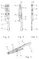
- the contact element 8 shown in Figs. 2-5 is provided as a one-piece, two-legged contact spring with a spring leg connection 14 and with mirror-inverted opposite contact tips 15 and is, as shown in Fig. 2, first by continuous punching from a metal band with a narrowed spring root 16 and widened spring legs 13 made. The contact element is then brought into the shape shown in FIGS. 3-5 by embossing.
- FIG. 6 shows a plug connection in which the knife contacts 5 of the mating connector 2 have not yet been inserted into the contact elements 8 of the connector 1. It can be seen that between the contact chamber walls 18 and the contact legs 13 due to a corresponding contour 17 there is a small distance (B). At the moment of inserting the knife contacts 5 of the mating connector 2 into the contact inlet (KE) of the contact elements 8, the spring legs 13 are deflected laterally with little force, 16 low insertion forces being achieved by the combination of a long effective spring length (l) and a narrow spring root.
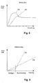
- the plug force curve of the plug connector is plotted over the insertion path in a diagram in FIG. 8. It can be seen that the plug-in force (SH) of a conventional connector has a much steeper course and also greater height than the plug-in force (SN) of a connector according to the invention.
- Fig. 9 the spring forces of the spring legs of a contact element of conventional design and a contact element / connector according to the invention are shown in a further diagram.
- the spring force (FH) of the spring legs increases linearly in conventional connectors
- the spring force (FN) of the spring legs of the contact element / connector according to the invention initially increases with a slight slope and rises steeply when the spring legs rest against the contact chamber walls.
Landscapes
- Coupling Device And Connection With Printed Circuit (AREA)
- Connector Housings Or Holding Contact Members (AREA)
Applications Claiming Priority (2)
| Application Number | Priority Date | Filing Date | Title |
|---|---|---|---|
| DE19820144 | 1998-05-06 | ||
| DE19820144A DE19820144C1 (de) | 1998-05-06 | 1998-05-06 | Elektrischer Steckverbinder |
Publications (2)
| Publication Number | Publication Date |
|---|---|
| EP0955693A2 true EP0955693A2 (fr) | 1999-11-10 |
| EP0955693A3 EP0955693A3 (fr) | 2000-11-15 |
Family
ID=7866800
Family Applications (1)
| Application Number | Title | Priority Date | Filing Date |
|---|---|---|---|
| EP99107527A Withdrawn EP0955693A3 (fr) | 1998-05-06 | 1999-04-15 | Connecteur électrique |
Country Status (4)
| Country | Link |
|---|---|
| US (1) | US6193561B1 (fr) |
| EP (1) | EP0955693A3 (fr) |
| CA (1) | CA2269753A1 (fr) |
| DE (1) | DE19820144C1 (fr) |
Families Citing this family (7)
| Publication number | Priority date | Publication date | Assignee | Title |
|---|---|---|---|---|
| DE19901962B4 (de) * | 1999-01-19 | 2006-05-11 | Erni Elektroapparate Gmbh | Verfahren zum Montieren elektrischer Steckverbindungen sowie Montagehilfe zur Verfahrensdurchführung |
| JP2002359033A (ja) * | 2001-05-31 | 2002-12-13 | Yazaki Corp | コネクタの嵌合構造 |
| JP2005141930A (ja) | 2003-11-04 | 2005-06-02 | Molex Inc | ケーブルコネクタ |
| TW200812156A (en) * | 2006-08-21 | 2008-03-01 | Speed Tech Corp | High destiny electrical connector and method for assembling thereof |
| DE102009030917B4 (de) * | 2009-06-25 | 2013-08-08 | Siemens Aktiengesellschaft | Elektrische Schaltanordnung |
| US8183155B1 (en) * | 2011-03-30 | 2012-05-22 | Hon Hai Precision Ind. Co., Ltd. | Lower profile connector assembly |
| US9444198B2 (en) * | 2014-03-04 | 2016-09-13 | Hitachi Metals, Ltd. | Communication module and communication module connector |
Family Cites Families (10)
| Publication number | Priority date | Publication date | Assignee | Title |
|---|---|---|---|---|
| DE1813739A1 (de) * | 1968-12-10 | 1970-06-25 | Schaltbau Gmbh | Steckverbindung,insbesondere fuer gedruckte Schaltungen |
| US3601775A (en) * | 1969-02-04 | 1971-08-24 | Amp Inc | Printed circuit connector |
| DE2125169B1 (de) * | 1971-05-21 | 1972-08-24 | Sauer H | Relais Steckkontaktfeder |
| US4033656A (en) * | 1975-09-02 | 1977-07-05 | Zero Manufacturing Company | Low profile integrated circuit socket |
| US4274700A (en) * | 1977-10-12 | 1981-06-23 | Bunker Ramo Corporation | Low cost electrical connector |
| DE9105347U1 (de) * | 1991-04-30 | 1992-09-03 | Panduit Gmbh, 6380 Bad Homburg | Steckverbinder |
| NL9200119A (nl) * | 1992-01-22 | 1993-08-16 | Du Pont Nederland | Connector met plaatvormige, interne afscherming. |
| JPH07230861A (ja) * | 1994-02-14 | 1995-08-29 | Whitaker Corp:The | ストラドル型コネクタ |
| US5807142A (en) * | 1996-05-10 | 1998-09-15 | Molex Incorporated | Electrical connector having terminals with improved retention means |
| US6048230A (en) * | 1996-11-25 | 2000-04-11 | Nec Corporation | Contact and high-density connector using the same |
-
1998
- 1998-05-06 DE DE19820144A patent/DE19820144C1/de not_active Expired - Fee Related
-
1999
- 1999-04-15 EP EP99107527A patent/EP0955693A3/fr not_active Withdrawn
- 1999-04-22 CA CA002269753A patent/CA2269753A1/fr not_active Abandoned
- 1999-05-05 US US09/305,582 patent/US6193561B1/en not_active Expired - Fee Related
Also Published As
| Publication number | Publication date |
|---|---|
| US6193561B1 (en) | 2001-02-27 |
| DE19820144C1 (de) | 2000-03-02 |
| EP0955693A3 (fr) | 2000-11-15 |
| CA2269753A1 (fr) | 1999-11-06 |
Similar Documents
| Publication | Publication Date | Title |
|---|---|---|
| DE69300865T2 (de) | Elektrischer verbinder mit blech als steckkontaktmaterial. | |
| DE69426133T2 (de) | Elektrische Kontaktstruktur mit geringer Einsteckkraft | |
| EP0793313B1 (fr) | Connecteur d'insérage à angle droit à insérer en force dans les trous d'un circuit imprimé | |
| DE2460848C2 (de) | Stromklemme | |
| DE19705509C2 (de) | Einstückige Kontaktfeder | |
| DE102009045550B4 (de) | Anschluss | |
| DE3888532T2 (de) | Fassungen für chipträger mit verbesserten kontakten. | |
| DE112013005813B4 (de) | Weiblicher Anschluss | |
| EP0353330B1 (fr) | Contact à douille | |
| DE102006017587A1 (de) | Federnd nachgiebiger Stift und elektrisches Bauteil zur Verwendung mit diesem federnd nachgiebigen Stift | |
| DE2460704A1 (de) | Elektrischer kontakt | |
| DE8508343U1 (de) | Überbrückter elektrischer Verbinder | |
| DE1465098A1 (de) | Elektrisches Verbindungsstueck | |
| DE2456977A1 (de) | Zugentlastung fuer leitungsanschluesse | |
| WO2005107019A1 (fr) | Broche pour liaison electrique sans etain comprenant une plaque conductrice, outil d'estampage et procede pour produire une liaison electrique sans etain | |
| DE102015211725B4 (de) | Verbinderanschluss und Verbinder hiermit | |
| DE4334088C2 (de) | Mehrpoliger Verbinder | |
| DE19820144C1 (de) | Elektrischer Steckverbinder | |
| DE19725966C1 (de) | Steckverbinder für Kartenrandmontage | |
| DE3925958C1 (en) | Plug connector insertable in metallised bores of PCB - has parallel rows of contact element at right angles to insertion direction of counter-plug for other appts. | |
| DE10308586B4 (de) | Verbinder zur Verbindung eines Paares parallel angeordneter Schaltplatinen | |
| DE69216212T2 (de) | Verbinder mit Haltemitteln | |
| EP1154521B1 (fr) | Connecteur et procédé de montage de connecteur | |
| DE19541953A1 (de) | Kontaktfeder | |
| DE9308142U1 (de) | Flachfederkontakt für eine Steckverbindung |
Legal Events
| Date | Code | Title | Description |
|---|---|---|---|
| PUAI | Public reference made under article 153(3) epc to a published international application that has entered the european phase |
Free format text: ORIGINAL CODE: 0009012 |
|
| AK | Designated contracting states |
Kind code of ref document: A2 Designated state(s): AT BE CH CY DE DK ES FI FR GB GR IE IT LI LU MC NL PT SE |
|
| AX | Request for extension of the european patent |
Free format text: AL;LT;LV;MK;RO;SI |
|
| PUAL | Search report despatched |
Free format text: ORIGINAL CODE: 0009013 |
|
| AK | Designated contracting states |
Kind code of ref document: A3 Designated state(s): AT BE CH CY DE DK ES FI FR GB GR IE IT LI LU MC NL PT SE |
|
| AX | Request for extension of the european patent |
Free format text: AL;LT;LV;MK;RO;SI |
|
| RIC1 | Information provided on ipc code assigned before grant |
Free format text: 7H 01R 13/11 A, 7H 01R 23/68 B, 7H 01R 13/41 B |
|
| STAA | Information on the status of an ep patent application or granted ep patent |
Free format text: STATUS: THE APPLICATION HAS BEEN WITHDRAWN |
|
| 18W | Application withdrawn |
Withdrawal date: 20010405 |