EP0962980A1 - Module micro-électronique hyperfréquences comportant deux matériaux de substrat différents et procédé de fabrication d'un tel module - Google Patents
Module micro-électronique hyperfréquences comportant deux matériaux de substrat différents et procédé de fabrication d'un tel module Download PDFInfo
- Publication number
- EP0962980A1 EP0962980A1 EP99401359A EP99401359A EP0962980A1 EP 0962980 A1 EP0962980 A1 EP 0962980A1 EP 99401359 A EP99401359 A EP 99401359A EP 99401359 A EP99401359 A EP 99401359A EP 0962980 A1 EP0962980 A1 EP 0962980A1
- Authority
- EP
- European Patent Office
- Prior art keywords
- substrate
- ferrite
- metallized
- carrier substrate
- carrier
- Prior art date
- Legal status (The legal status is an assumption and is not a legal conclusion. Google has not performed a legal analysis and makes no representation as to the accuracy of the status listed.)
- Granted
Links
Images


Classifications
-
- H—ELECTRICITY
- H10—SEMICONDUCTOR DEVICES; ELECTRIC SOLID-STATE DEVICES NOT OTHERWISE PROVIDED FOR
- H10W—GENERIC PACKAGES, INTERCONNECTIONS, CONNECTORS OR OTHER CONSTRUCTIONAL DETAILS OF DEVICES COVERED BY CLASS H10
- H10W44/00—Electrical arrangements for controlling or matching impedance
- H10W44/20—Electrical arrangements for controlling or matching impedance at high-frequency [HF] or radio frequency [RF]
-
- H—ELECTRICITY
- H10—SEMICONDUCTOR DEVICES; ELECTRIC SOLID-STATE DEVICES NOT OTHERWISE PROVIDED FOR
- H10W—GENERIC PACKAGES, INTERCONNECTIONS, CONNECTORS OR OTHER CONSTRUCTIONAL DETAILS OF DEVICES COVERED BY CLASS H10
- H10W70/00—Package substrates; Interposers; Redistribution layers [RDL]
- H10W70/60—Insulating or insulated package substrates; Interposers; Redistribution layers
- H10W70/67—Insulating or insulated package substrates; Interposers; Redistribution layers characterised by their insulating layers or insulating parts
- H10W70/68—Shapes or dispositions thereof
- H10W70/681—Shapes or dispositions thereof comprising holes not having chips therein, e.g. for outgassing, underfilling or bond wire passage
-
- H—ELECTRICITY
- H10—SEMICONDUCTOR DEVICES; ELECTRIC SOLID-STATE DEVICES NOT OTHERWISE PROVIDED FOR
- H10W—GENERIC PACKAGES, INTERCONNECTIONS, CONNECTORS OR OTHER CONSTRUCTIONAL DETAILS OF DEVICES COVERED BY CLASS H10
- H10W72/00—Interconnections or connectors in packages
- H10W72/50—Bond wires
- H10W72/531—Shapes of wire connectors
- H10W72/5363—Shapes of wire connectors the connected ends being wedge-shaped
-
- H—ELECTRICITY
- H10—SEMICONDUCTOR DEVICES; ELECTRIC SOLID-STATE DEVICES NOT OTHERWISE PROVIDED FOR
- H10W—GENERIC PACKAGES, INTERCONNECTIONS, CONNECTORS OR OTHER CONSTRUCTIONAL DETAILS OF DEVICES COVERED BY CLASS H10
- H10W72/00—Interconnections or connectors in packages
- H10W72/50—Bond wires
- H10W72/551—Materials of bond wires
- H10W72/552—Materials of bond wires comprising metals or metalloids, e.g. silver
- H10W72/5522—Materials of bond wires comprising metals or metalloids, e.g. silver comprising gold [Au]
Definitions
- the present invention relates to micro-electronic modules microwave with two different substrate materials in one thick layer interconnection structure.
- the invention also relates to method of manufacturing such a module and more precisely the manufacture of metallized substrate of the module.
- Modern micro-electronic modules allow perform various electronic functions by combining on a substrate various components such as resistors, capacitors, diodes, transistors, microwave integrated circuits etc.
- the substrate can be of ceramic or glass type and has the connections electrical and all or part of the passive components produced for example by thick layer techniques.
- these microelectronic modules use in a microstrip technology operating up to 20 GHz, two substrates made of different materials, generally an alumina substrate (Al 2 O 3 ) of 99.6% purity and a substrate ferrite.
- the alumina substrate (Al 2 O 3 ) receives the functions of oscillator, amplifier, filter type, the ferrite substrate receiving the functions of isolator, circulator.
- FIG. 1 shows a microelectronic module 10 Microwaves according to the prior art comprising two substrates in different materials, an alumina substrate 12 (or carrier substrate in alumina) and a ferrite substrate 14, integrated in a case 16 made of titanium.
- the alumina substrate 12 has metallizations 18 on each of its two opposite faces, and in the same way the ferrite substrate has metallizations 20.
- the metallizations of the two substrates are made in thick layer technology.
- the two substrates metallized are produced separately according to known techniques.
- FIG. 2a shows the alumina substrate 12 in which is made a passage 30 of circular shape by CO2 laser cutting so to receive the ferrite substrate 14 in the form of a circular plate of dimension substantially identical to that of passage 30.
- the tolerances of fabrications of passage 30 and of ferrite substrate 14 are such that the substrate 14 can be inserted into passage 30 without difficulty.
- the figure 2b shows a sectional view, along an axis AA ', showing the passage 30 of the alumina substrate of FIG. 2a.
- FIG. 3a shows the ferrite substrate 14 comprising the metallizations 20.
- FIG. 3b represents a sectional view along an axis BB 'of the ferrite substrate of Figure 3a.
- a small permanent magnet is arranged on the ferrite substrate in a known manner in order to perform the function isolator or circulator necessary for the operation of the microelectronic module of figure 1.
- the microelectronic module can be more complex than that represents in example in FIG. 1 which can comprise several substrates ferrites.
- FIG. 1 which can comprise several substrates ferrites.
- microwave micro-electronic modules comprises two separate screen printing operations for the metallization of substrates in different materials and involves wired micro-wiring of the electrical interconnections between these substrates, long and delicate and therefore expensive.
- the present invention solves the double problem of separate screen printing of substrates made of different materials and interconnection by wire micro-wiring between the substrates by proposing a microwave micro-electronic module comprising a carrier substrate and a ferrite substrate separated by a gap, each substrate having at at least one metallized face, a first metallized face of the carrier substrate and a first metallized face of the ferrite substrate being located in a same foreground, the two substrates being located on the same side of this foreground, characterized in that the ferrite substrate is fixed to the substrate carrier by a material located in the gap and which outcrops in the foreground, the carrier substrate, the ferrite substrate and the material, forming a unique metallized substrate, the material where it is exposed in the foreground being covered by a metallization ensuring electrical interconnection between those of the metallized faces of the carrier substrate and the ferrite substrate which are located in the foreground.
- the carrier substrate and the ferrite substrate are of the same thickness and each have a second metallized face, respectively a second metallized face of the carrier substrate and a second metallized face of ferrite substrate.
- These second metallized faces are located in a same background, and the material located in the interstice and which is exposed in the second plane is covered by a metallization located in this second plan ensuring the electrical interconnection between those of the metallized faces of the carrier substrate and the ferrite substrate which are located in the second plan.
- the single substrate includes metallizations on its two faces located respectively on the first and the second plane.
- the material located in the gap is a dielectric sealing paste, for example a dielectric sealing glass.
- This dough must have a coefficient of compatible K dilation, that is to say of close value and of the same sign, that the expansion coefficients K1 of the carrier substrate and K2 of the substrate ferrite, in order to obtain a reliable fixing of the ferrite substrate to the substrate carrier.
- the production according to the invention of a single metallized substrate eliminates at least two important and costly operations necessary in the manufacturing processes of the prior art, the bonding of the ferrite substrate in the module housing and interconnection by wire micro-wiring between the metallizations of the two substrates.
- the integration in the housing of the micro-electronic module of the single substrate constituted by the carrier substrate the ferrite substrate and the filling material of the gap between the two substrates is made of a single operation unlike the manufacturing process according to art previous which requires as described above at least two operations, one for each of the substrates, consisting of a first integration operation in the housing of the metallized alumina substrate then a second integration operation in the housing of the ferrite substrate metallic.
- Another advantage of the module manufacturing process according to the invention lies in the sole metallization operation of the substrate and the removal of the wired micro-wiring required in the manufacture of modules according to the prior art. Indeed only one operation collective metallization in a thick layer of the single substrate allows metallizing the carrier substrate, the ferrite substrate attached to the carrier substrate and material located in the gap flush with the level faces of the single substrate, which ensures electrical interconnection between the metallizations of the carrier substrate and those of the ferrite substrate.
- FIG. 4 represents an electronic module 40 according to the invention comprising a single substrate 42 metallized on its two faces and produced at from an alumina carrier substrate 44 and an integrated ferrite substrate 46 or sealed to the carrier substrate in a circular recess 50 made in the alumina carrier substrate, the carrier substrate and the ferrite substrate having substantially the same thickness.
- Each substrate has a first side and a second side opposite the first, respectively a first face 51 and a second face 52 of the carrier substrate and a first face 53 and a second face 54 of the ferrite substrate.
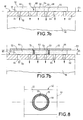
- the device 60 comprises a plate 62 having holes suction 64 opening on one side of the plate into an enclosure 66 in air depression Dp in relation to the ambient environment and on the other side of the plate, in a foreground P1, in the ambient environment.
- the alumina-bearing substrate 44 is placed by its first face 51 on the foreground P1, on the other side of the plate 62, at the pressure ambient, on the suction holes 64.
- the carrier substrate is maintained applied against the plate by the depression Dp through the holes 64.
- the ferrite substrate 46 is placed in succession in the recess 50 of the carrier substrate, its first face 53 being applied against the plate 62 on the foreground P1.
- the ferrite substrate is in turn maintained in position against the plate by the depression Dp through the holes 64
- the two substrates having the same thickness, the second face 52 of the carrier substrate and the second face 54 of the ferrite substrate are located on the same second plane P2 represents in FIG. 7b.
- a gap 68 appears between the carrier substrate alumina 44 and the ferrite substrate 46 positioned in the recess 50.
- a dielectric sealing paste 70 for example glass of sealing, is then deposited in the gap 68 using a screen serigraph 72
- the sealing compound must have a coefficient of expansion K compatible with the coefficient of expansion K1 of the carrier substrate and the coefficient of expansion K2 of the ferrite substrate.
- fixing the substrate ferrite 46 to the carrier substrate 44 by the dielectric sealing glass is obtained by baking at about a temperature of 850 ° C, forming the single substrate 42.
- Figure 9a shows a section of the single substrate 42 after metallization and FIG. 9b a view of one of its metallized faces.
- Metallizations 80 are deposited on both sides of the single substrate 42 thus achieving in a single operation the metallization of the alumina carrier substrate 44, ferrite substrate 46 and the metallizations of the sealing glass 70 located at the gap 68.
- An industrial gain is also obtained on the cost of production of the module by the reduction in the cost linked to the manufacture of the single substrate and the simplification of its mounting in the module housing.
- the cycle of module manufacturing can be lowered by at least an hour thanks to the elimination of the manual operation of mounting the ferrite substrate in the housing and the elimination of the wired wiring of the modules of the prior art.
- micro-electronic module shown in example in Figure 4 is not limiting. More complex modules using a carrier substrate and several ferrite substrates sealed in the carrier substrate according to the invention, in order to produce circulators or insulators microwaves can integrate passive elements produced by thick film techniques, for example screen-printed resistors from a paste made from Rhutenium dioxide, but also from chips and integrated circuits transferred onto the substrate according to known techniques.
- micro-electronic modules according to the invention provides better stability of the module's microwave performance and very good resistance to rapid temperature variations which can be between approximately -55 ° C and + 125 ° C,
Landscapes
- Non-Reversible Transmitting Devices (AREA)
- Parts Printed On Printed Circuit Boards (AREA)
Abstract
- réalisation du substrat porteur (44) et du substrat ferrite (46), non métallisés.
- fixation du substrat ferrite (46) au substrat porteur (44) par une matière (70) remplissant l'interstice entre le substrat porteur et le substrat ferrite, formant le substrat unique (42).
- métallisation du substrat unique.
Description
- collage du substrat d'alumine 12 dans le boítier 16 par un film 22 tramé conducteur électrique préimpreigné de colle conductrice, puis polymérisation à chaud de la colle rendant le substrat en alumine 12 solidaire du boítier 16.
- collage du substrat ferrite 14 avec de la colle conductrice 24 dans le fond du boítier 16, le substrat ferrite 14 étant positionné préalablement à la main à l'intérieur de l'évidement 30 du substrat en alumine 12.
- réalisation des interconnexions électriques entre les métallisations 18 du substrat en alumine 12 et les métallisations 20 du substrat ferrite 14 par microcâblage de fils 32 en or d'un diamètre d'environ 25 micromètres. Le microcâblage des fils 32 est réalisé par ultrasons, thermo-compression ou soudure électrique.
- réalisation du substrat porteur et du substrat ferrite.
- fixation du substrat ferrite au substrat porteur par une matière remplissant l'interstice entre le substrat porteur et le substrat ferrite, la première face du substrat porteur et la première face du substrat ferrite étant situées dans le même premier plan, les deux substrats étant situés d'un même coté du premier plan.
- métallisation d'au moins la face du substrat unique située dans le premier plan.
- la figure 1 représente un module micro-électronique, déjà décrit, selon l'art antérieur.
- les figures 2a,2b,3a,3b des vues du substrat d'alumine et du substrat ferrite du module de la figure 1, selon l'art antérieur.
- la figure 4 représente un module micro-électronique selon l'invention.
- les figures 5a,5b,6a,6b, des vues du substrat en porteur et du substrat ferrite du module de la figure 4 selon l'invention.
- les figures 7a et 7b montrent un dispositif utilisé pour la fixation du substrat ferrite au substrat porteur.
- la figure 8 montre le substrat unique du module de la figure 4 selon l'invention.
- les figures 9a et 9b montrent le substrat unique métallisé du module de la figure 4 selon l'invention.
- réalisation du substrat porteur en alumine 44 selon des techniques connues, comportant un passage 50 de forme circulaire permettant le scellement du substrat ferrite 46 dans le substrat porteur en alumine 44. Le passage 50 peut être réalisé par une découpe au laser C02 du substrat porteur.
- réalisation du substrat ferrite 46 en forme de pastille circulaire de diamètre sensiblement identique à celui du passage 50. Les tolérances de fabrications du passage 50 et du substrat ferrite 46 sont telles que ce dernier puisse être inséré dans le passage 50 sans difficulté. Par exemple dans cette réalisation les tolérances sur le diamètre de découpe du passage circulaire dans le substrat porteur sont de 0µm, +20µm et les tolérances sur le diamètre du substrat ferrite sont de 0µm, -20µm.
- fixation du substrat ferrite 46 dans le substrat porteur 44 en alumine. A cet effet on utilise un dispositif 60 représenté aux figures 7a et 7b.
- métallisation du substrat unique 42 selon les techniques connues en couche épaisse.
- fixation du substrat unique métallisé selon des méthodes connues dans le boítier 16, par exemple par collage par un film tramé conducteur électrique préimpregné de colle conductrice.
Claims (12)
- Module micro-électronique hyperfréquences comportant un substrat porteur (12,44) et un substrat ferrite (14,46) séparés par un interstice (26,68), chaque substrat ayant au moins face métallisée, une première face (51) métallisée du substrat porteur et une première face (53) métallisée du substrat ferrite étant situées dans un même premier plan (P1), les deux substrats étant situés d'un même coté de ce premier plan, caractérisé en ce que le substrat ferrite (46) est fixé au substrat porteur (44) par une matière (70) située dans l'interstice (68) et qui affleure dans le premier plan (P1), le substrat porteur, le substrat ferrite et la matière, formant un substrat unique (42) métallisé, la matière là où elle affleure dans le premier plan (P1) étant recouverte par une métallisation (76) assurant l'interconnexion électrique entre celles (80) des faces métallisées du substrat porteur et du substrat ferrite qui sont situées dans le premier plan (P1).
- Module micro-électronique selon la revendication 1, caractérisé en ce que le substrat porteur (12,44) et le substrat ferrite (14,46) sont de même épaisseur et comportent chacun une seconde face métallisée, respectivement une seconde face métallisée (52) du substrat porteur et une seconde face métallisée (54) du substrat ferrite, ces secondes faces métallisées étant situées dans un même second plan (P2), et en ce que la matière (70) située dans l'interstice (68) et qui affleure dans le second plan (P2) est recouverte par une métallisation (74) située dans ce second plan assurant l'interconnexion électrique entre celles (80) des faces métallisées du substrat porteur et du substrat ferrite qui sont situées dans le second plan (P2).
- Module micro-électronique hyperfréquences selon l'une des revendications 1 ou 2, caractérisé en ce que le substrat porteur (12,44) est un substrat en alumine.
- Module micro-électronique hyperfréquences selon l'une des revendications 1 à 3, caractérisé en en ce que la matière (70) est une pâte de scellement présentant un coefficient de dilatation K compatible avec le coefficient de dilatation K1 du substrat porteur et le coefficient de dilatation K2 du substrat ferrite.
- Module micro-électronique hyperfréquences selon la revendication 4, caractérisé en en ce que :le coefficient de dilatation K de la pâte de scellement diélectrique est compris entre environ 7.10-6/°C et 8.10-6/°C,que le coefficient de dilatation K1 du substrat porteur en alumine (Al2O3) est d'environ 7.10-6/°C,et en ce que le coefficient de dilatation K2 du substrat ferrite est compris entre environ 6.10-6/°C et 7.10-6/°C.
- Module micro-électronique hyperfréquences selon l'une des revendications 3 à 5, caractérisé en en ce que le substrat porteur en alumine (44) comporte un passage (50) de forme circulaire permettant le scellement d'un substrat ferrite (46) dans le substrat porteur en alumine (44), le substrat ferrite étant en forme de pastille circulaire de diamètre sensiblement identique à celui du passage (50).
- Procédé de fabrication d'un module micro-électronique hyperfréquences selon l'une quelconque des revendications précédentes, caractérisé en ce qu'il comporte au moins les étapes suivantes:réalisation du substrat porteur (44) et du substrat ferrite (46), non métallisés.fixation du substrat ferrite (46) au substrat porteur (44) par une matière (70) remplissant l'interstice (68) entre le substrat porteur et le substrat ferrite, formant un substrat unique (42), la première face (51) du substrat porteur et la première face (53) du substrat ferrite étant situées dans le même premier plan (P1), les deux substrats étant situés d'un même coté du premier plan (P1).métallisation d'au moins la face du substrat unique située dans le premier plan.
- Procédé de fabrication d'un module micro-électronique hyperfréquences selon la revendication 7 caractérisée en ce que matière (70) remplissant l'interstice (68) entre le substrat porteur et le substrat ferrite est une pâte diélectrique et en ce que le remplissage de l'interstice (68) est effectué l'aide un écran de sérigraphie (72).
- Procédé de fabrication d'un module micro-électronique hyperfréquences selon la revendication 8 caractérisée en ce que la pâte est un verre de scellement diélectrique.
- Procédé de fabrication d'un module micro-électronique hyperfréquences selon la revendication 9, caractérisée en ce que, après séchage du verre de scellement, la fixation du substrat ferrite (46) au substrat porteur (44) par le verre de scellement diélectrique est obtenu, par une cuisson à environ une température de 850°C, formant le substrat unique (42).
- Procédé de fabrication d'un module micro-électronique hyperfréquences selon l'une des revendications 7 à 10, caractérisée en ce que la métallisation (80) du substrat unique est effectuée selon la technologie de couche épaisse.
- Procédé de fabrication d'un module micro-électronique hyperfréquences selon l'une des revendications 7 à 11, caractérisée en ce que le passage (50) de forme circulaire permettant le scellement du substrat ferrite (46) dans le substrat porteur en alumine (44) est réalisé par une découpe au laser C02 du substrat porteur en alumine.
Applications Claiming Priority (2)
| Application Number | Priority Date | Filing Date | Title |
|---|---|---|---|
| FR9807096A FR2779576B1 (fr) | 1998-06-05 | 1998-06-05 | Module micro-electronique hyperfrequences comportant deux materiaux de substrat differents et procede de fabrication d'un tel module |
| FR9807096 | 1998-06-05 |
Publications (2)
| Publication Number | Publication Date |
|---|---|
| EP0962980A1 true EP0962980A1 (fr) | 1999-12-08 |
| EP0962980B1 EP0962980B1 (fr) | 2006-12-27 |
Family
ID=9527062
Family Applications (1)
| Application Number | Title | Priority Date | Filing Date |
|---|---|---|---|
| EP99401359A Expired - Lifetime EP0962980B1 (fr) | 1998-06-05 | 1999-06-04 | Module micro-électronique hyperfréquences comportant deux matériaux de substrat différents et procédé de fabrication d'un tel module |
Country Status (4)
| Country | Link |
|---|---|
| EP (1) | EP0962980B1 (fr) |
| DE (1) | DE69934542T2 (fr) |
| ES (1) | ES2280114T3 (fr) |
| FR (1) | FR2779576B1 (fr) |
Cited By (1)
| Publication number | Priority date | Publication date | Assignee | Title |
|---|---|---|---|---|
| WO2002043146A1 (fr) * | 2000-11-21 | 2002-05-30 | Kerafol Keramische Folien Gmbh | Pellicule de ferrite |
Citations (2)
| Publication number | Priority date | Publication date | Assignee | Title |
|---|---|---|---|---|
| EP0197476A2 (fr) * | 1985-04-03 | 1986-10-15 | ANT Nachrichtentechnik GmbH | Circulateur à micro-ondes |
| US5745981A (en) * | 1993-04-01 | 1998-05-05 | General Electric Company | Method for making magnetic and electromagnetic circuit components having embedded magnetic materials in a high density interconnect structure |
-
1998
- 1998-06-05 FR FR9807096A patent/FR2779576B1/fr not_active Expired - Fee Related
-
1999
- 1999-06-04 DE DE69934542T patent/DE69934542T2/de not_active Expired - Lifetime
- 1999-06-04 ES ES99401359T patent/ES2280114T3/es not_active Expired - Lifetime
- 1999-06-04 EP EP99401359A patent/EP0962980B1/fr not_active Expired - Lifetime
Patent Citations (2)
| Publication number | Priority date | Publication date | Assignee | Title |
|---|---|---|---|---|
| EP0197476A2 (fr) * | 1985-04-03 | 1986-10-15 | ANT Nachrichtentechnik GmbH | Circulateur à micro-ondes |
| US5745981A (en) * | 1993-04-01 | 1998-05-05 | General Electric Company | Method for making magnetic and electromagnetic circuit components having embedded magnetic materials in a high density interconnect structure |
Non-Patent Citations (1)
| Title |
|---|
| H. TOMIMURO ET AL.: "Reliability study on microwave integrated circuits for the 20G-D2 transmission systems", REVIEW OF THE ELECTRICAL COMMUNICATION LABORATORIES, vol. 32, no. 6, November 1984 (1984-11-01), tokyo,JP, pages 1100 - 1106, XP002093322 * |
Cited By (1)
| Publication number | Priority date | Publication date | Assignee | Title |
|---|---|---|---|---|
| WO2002043146A1 (fr) * | 2000-11-21 | 2002-05-30 | Kerafol Keramische Folien Gmbh | Pellicule de ferrite |
Also Published As
| Publication number | Publication date |
|---|---|
| ES2280114T3 (es) | 2007-09-01 |
| DE69934542T2 (de) | 2007-10-25 |
| EP0962980B1 (fr) | 2006-12-27 |
| FR2779576A1 (fr) | 1999-12-10 |
| FR2779576B1 (fr) | 2001-04-27 |
| DE69934542D1 (de) | 2007-02-08 |
Similar Documents
| Publication | Publication Date | Title |
|---|---|---|
| US7692292B2 (en) | Packaged electronic element and method of producing electronic element package | |
| EP0638933B1 (fr) | Procédé d'interconnexion de pastilles semi-conductrices en trois dimensions, et composant en résultant | |
| CA2321360C (fr) | Procede d'encapsulation de composants electroniques | |
| EP0321340B1 (fr) | Support de composant électronique, notamment pour carte mémoire, et produit ainsi obtenu | |
| EP3089211B1 (fr) | Procede d'encapsulation d'un circuit electronique | |
| CA2320343A1 (fr) | Composant a ondes de surface encapsule et procede de fabrication collective | |
| EP0044247B1 (fr) | Procédé de fabrication d'un support de composants électroniques pour la connexion des supports de puces de circuits intégrés | |
| FR2635920A1 (fr) | Procede de fabrication d'une zone de connexion pour un circuit hyperfrequence de type triplaque et circuit ainsi obtenu | |
| EP0962980B1 (fr) | Module micro-électronique hyperfréquences comportant deux matériaux de substrat différents et procédé de fabrication d'un tel module | |
| EP1964204B1 (fr) | Boitier avec fonction accordable en frequence | |
| EP1657749B1 (fr) | Boîtier microélectronique multiplans avec blindage interne | |
| EP0334747A1 (fr) | Dispositif d'interconnexion et de protection d'une pastille nue de composant hyperfréquence | |
| FR2565030A1 (fr) | Structure de metallisations de reprise de contacts d'un dispositif semi-conducteur et dispositif dote d'une telle structure | |
| FR2495837A1 (fr) | Embase de microboitier d'encapsulation et microboitier comportant une telle embase | |
| EP0586010B1 (fr) | Circuit pour des fréquences élevées, et procédé pour le réaliser | |
| FR2529386A1 (fr) | Boitier de circuit electronique comportant un condensateur | |
| FR2529385A1 (fr) | Microboitier d'encapsulation de circuits integres logiques fonctionnant en tres haute frequence | |
| EP1557394B1 (fr) | Dispositif et procédé pour assurer l'herméticité d'une cavité dans laquelle débouche un passage | |
| EP2688137B1 (fr) | Résonateur hyperfréquence a saut d'impédance, notamment pour filtres hyperfréquence coupe-bande ou passe-bande | |
| FR2633789A1 (fr) | Filtre compact a resonateurs utilisant l'effet piezoelectrique | |
| FR2507017A1 (fr) | Microassemblage utilisable en hyperfrequences | |
| FR2843485A1 (fr) | Procede de fabrication d'un module de circuits integres et module correspondant | |
| FR2674682A1 (fr) | Module hybride et procede de realisation. | |
| FR2758417A1 (fr) | Boitier d'encapsulation de composant hyperfrequence, et procede d'obtention | |
| WO2020012101A1 (fr) | Procede de fabrication d'un module electronique de puissance pour une électronique embarquée sur aeronef |
Legal Events
| Date | Code | Title | Description |
|---|---|---|---|
| PUAI | Public reference made under article 153(3) epc to a published international application that has entered the european phase |
Free format text: ORIGINAL CODE: 0009012 |
|
| AK | Designated contracting states |
Kind code of ref document: A1 Designated state(s): DE ES FI FR GB GR IT SE |
|
| AX | Request for extension of the european patent |
Free format text: AL;LT;LV;MK;RO;SI |
|
| 17P | Request for examination filed |
Effective date: 20000412 |
|
| AKX | Designation fees paid |
Free format text: DE ES FI FR GB GR IT SE |
|
| RAP1 | Party data changed (applicant data changed or rights of an application transferred) |
Owner name: THALES |
|
| GRAP | Despatch of communication of intention to grant a patent |
Free format text: ORIGINAL CODE: EPIDOSNIGR1 |
|
| GRAS | Grant fee paid |
Free format text: ORIGINAL CODE: EPIDOSNIGR3 |
|
| GRAA | (expected) grant |
Free format text: ORIGINAL CODE: 0009210 |
|
| AK | Designated contracting states |
Kind code of ref document: B1 Designated state(s): DE ES FI FR GB GR IT SE |
|
| REG | Reference to a national code |
Ref country code: GB Ref legal event code: FG4D Free format text: NOT ENGLISH |
|
| REF | Corresponds to: |
Ref document number: 69934542 Country of ref document: DE Date of ref document: 20070208 Kind code of ref document: P |
|
| REG | Reference to a national code |
Ref country code: SE Ref legal event code: TRGR |
|
| REG | Reference to a national code |
Ref country code: GR Ref legal event code: EP Ref document number: 20070400947 Country of ref document: GR |
|
| REG | Reference to a national code |
Ref country code: ES Ref legal event code: FG2A Ref document number: 2280114 Country of ref document: ES Kind code of ref document: T3 |
|
| PLBE | No opposition filed within time limit |
Free format text: ORIGINAL CODE: 0009261 |
|
| STAA | Information on the status of an ep patent application or granted ep patent |
Free format text: STATUS: NO OPPOSITION FILED WITHIN TIME LIMIT |
|
| 26N | No opposition filed |
Effective date: 20070928 |
|
| REG | Reference to a national code |
Ref country code: FR Ref legal event code: PLFP Year of fee payment: 17 |
|
| PGFP | Annual fee paid to national office [announced via postgrant information from national office to epo] |
Ref country code: GB Payment date: 20150603 Year of fee payment: 17 Ref country code: DE Payment date: 20150527 Year of fee payment: 17 Ref country code: ES Payment date: 20150527 Year of fee payment: 17 Ref country code: FI Payment date: 20150609 Year of fee payment: 17 Ref country code: SE Payment date: 20150611 Year of fee payment: 17 |
|
| PGFP | Annual fee paid to national office [announced via postgrant information from national office to epo] |
Ref country code: GR Payment date: 20150529 Year of fee payment: 17 Ref country code: FR Payment date: 20150608 Year of fee payment: 17 |
|
| PGFP | Annual fee paid to national office [announced via postgrant information from national office to epo] |
Ref country code: IT Payment date: 20150625 Year of fee payment: 17 |
|
| REG | Reference to a national code |
Ref country code: DE Ref legal event code: R119 Ref document number: 69934542 Country of ref document: DE |
|
| PG25 | Lapsed in a contracting state [announced via postgrant information from national office to epo] |
Ref country code: FI Free format text: LAPSE BECAUSE OF NON-PAYMENT OF DUE FEES Effective date: 20160604 |
|
| REG | Reference to a national code |
Ref country code: SE Ref legal event code: EUG |
|
| PG25 | Lapsed in a contracting state [announced via postgrant information from national office to epo] |
Ref country code: SE Free format text: LAPSE BECAUSE OF NON-PAYMENT OF DUE FEES Effective date: 20160605 |
|
| GBPC | Gb: european patent ceased through non-payment of renewal fee |
Effective date: 20160604 |
|
| REG | Reference to a national code |
Ref country code: GR Ref legal event code: ML Ref document number: 20070400947 Country of ref document: GR Effective date: 20170109 |
|
| REG | Reference to a national code |
Ref country code: FR Ref legal event code: ST Effective date: 20170228 |
|
| PG25 | Lapsed in a contracting state [announced via postgrant information from national office to epo] |
Ref country code: FR Free format text: LAPSE BECAUSE OF NON-PAYMENT OF DUE FEES Effective date: 20160630 Ref country code: DE Free format text: LAPSE BECAUSE OF NON-PAYMENT OF DUE FEES Effective date: 20170103 Ref country code: GR Free format text: LAPSE BECAUSE OF NON-PAYMENT OF DUE FEES Effective date: 20170109 |
|
| PG25 | Lapsed in a contracting state [announced via postgrant information from national office to epo] |
Ref country code: GB Free format text: LAPSE BECAUSE OF NON-PAYMENT OF DUE FEES Effective date: 20160604 |
|
| PG25 | Lapsed in a contracting state [announced via postgrant information from national office to epo] |
Ref country code: IT Free format text: LAPSE BECAUSE OF NON-PAYMENT OF DUE FEES Effective date: 20160604 |
|
| REG | Reference to a national code |
Ref country code: ES Ref legal event code: FD2A Effective date: 20180507 |
|
| PG25 | Lapsed in a contracting state [announced via postgrant information from national office to epo] |
Ref country code: ES Free format text: LAPSE BECAUSE OF NON-PAYMENT OF DUE FEES Effective date: 20160605 |