EP0998084B1 - Démodulateur et procédé de démodulation de signaux MDP qui employent une technique de fenêtrage de la largeur de la période - Google Patents
Démodulateur et procédé de démodulation de signaux MDP qui employent une technique de fenêtrage de la largeur de la période Download PDFInfo
- Publication number
- EP0998084B1 EP0998084B1 EP99308181A EP99308181A EP0998084B1 EP 0998084 B1 EP0998084 B1 EP 0998084B1 EP 99308181 A EP99308181 A EP 99308181A EP 99308181 A EP99308181 A EP 99308181A EP 0998084 B1 EP0998084 B1 EP 0998084B1
- Authority
- EP
- European Patent Office
- Prior art keywords
- output
- signal
- demodulator
- carrier
- communications signal
- Prior art date
- Legal status (The legal status is an assumption and is not a legal conclusion. Google has not performed a legal analysis and makes no representation as to the accuracy of the status listed.)
- Expired - Lifetime
Links
- 238000000034 method Methods 0.000 title claims description 20
- 238000004891 communication Methods 0.000 claims description 102
- 230000010363 phase shift Effects 0.000 claims description 56
- 230000007704 transition Effects 0.000 claims description 50
- 230000008859 change Effects 0.000 claims description 8
- 238000003860 storage Methods 0.000 claims description 6
- 230000000694 effects Effects 0.000 claims description 5
- 230000002123 temporal effect Effects 0.000 claims description 4
- 230000011664 signaling Effects 0.000 claims 2
- 238000004519 manufacturing process Methods 0.000 description 9
- 230000036039 immunity Effects 0.000 description 4
- 230000035945 sensitivity Effects 0.000 description 4
- 230000001960 triggered effect Effects 0.000 description 4
- 238000005259 measurement Methods 0.000 description 3
- 238000012545 processing Methods 0.000 description 3
- 238000005516 engineering process Methods 0.000 description 2
- 238000011156 evaluation Methods 0.000 description 2
- 238000012986 modification Methods 0.000 description 2
- 230000004048 modification Effects 0.000 description 2
- 230000000630 rising effect Effects 0.000 description 2
- 230000002238 attenuated effect Effects 0.000 description 1
- 230000009286 beneficial effect Effects 0.000 description 1
- 230000015556 catabolic process Effects 0.000 description 1
- 238000002485 combustion reaction Methods 0.000 description 1
- 238000006731 degradation reaction Methods 0.000 description 1
- 230000002939 deleterious effect Effects 0.000 description 1
- 238000013461 design Methods 0.000 description 1
- 238000001514 detection method Methods 0.000 description 1
- 238000010586 diagram Methods 0.000 description 1
- 238000009826 distribution Methods 0.000 description 1
- 238000009432 framing Methods 0.000 description 1
- 230000010354 integration Effects 0.000 description 1
- 230000007246 mechanism Effects 0.000 description 1
- 230000009467 reduction Effects 0.000 description 1
- 230000001360 synchronised effect Effects 0.000 description 1
Images


Classifications
-
- H—ELECTRICITY
- H04—ELECTRIC COMMUNICATION TECHNIQUE
- H04L—TRANSMISSION OF DIGITAL INFORMATION, e.g. TELEGRAPHIC COMMUNICATION
- H04L27/00—Modulated-carrier systems
- H04L27/18—Phase-modulated carrier systems, i.e. using phase-shift keying
- H04L27/22—Demodulator circuits; Receiver circuits
-
- H—ELECTRICITY
- H04—ELECTRIC COMMUNICATION TECHNIQUE
- H04L—TRANSMISSION OF DIGITAL INFORMATION, e.g. TELEGRAPHIC COMMUNICATION
- H04L27/00—Modulated-carrier systems
- H04L27/18—Phase-modulated carrier systems, i.e. using phase-shift keying
- H04L27/22—Demodulator circuits; Receiver circuits
- H04L27/233—Demodulator circuits; Receiver circuits using non-coherent demodulation
- H04L27/2335—Demodulator circuits; Receiver circuits using non-coherent demodulation using temporal properties of the received signal
- H04L27/2337—Demodulator circuits; Receiver circuits using non-coherent demodulation using temporal properties of the received signal using digital techniques to measure the time between zero-crossings
Definitions
- the present invention relates generally to demodulators for communications equipment and, in particular, to demodulators for phase-shift-keyed or analogous communications signals.
- Phase-shift-keying (PSK) demodulators often have used inflexible fixed-function circuitry limited to particular applications. Consequently, new or different applications have required designing new circuitry for particular applications, which tended to increase costs of the demodulators.
- PSK Phase-shift-keying
- ASIC Application Specific Integrated Circuits
- PLL phase locked loops
- An ASIC may comprise a dedicated algorithm to recover the message content of a received signal.
- a PLL comprises an oscillator control mechanism that limits the practical frequency range of demodulators. While the frequency range of a PLL circuit may be enhanced by using adjustable components or replacing components, such hardware changes may require disassembly of the PLL circuit, its housing, or other disruptive measures. Thus, a need exists for a cost-effective demodulator that is readily apposite to a wide assortment of applications.
- Fleek discloses a PSK demodulator which operates at a given frequency by counting a predetermined number of pulses for a measured clock count value.
- the demodulator disclosed therein determines when the spacing between peaks of a square wave change due to phase-shift-keying. This square wave is output by a digital filter which helps distinguish transitory events in a waveform from being confused with disturbances.
- Inter-message noise refers to electromagnetic noise energy between PSK messages.
- Inter-message noise may be modeled as a randomly occurring electromagnetic signal with an amplitude characterized by a probability density function. Inter-message noise tends to degrade reception of PSK messages and interpretation of demodulated data.
- a demodulator with insufficient immunity to noise is characterized by an unacceptably high frequency of false phase shift detections.
- some electronic manufacturers have attenuated the received signal at the PSK demodulator.
- an unwanted side effect of such attenuation is reduced sensitivity of the demodulator, which may make weaker received signals incapable of being properly detected.
- a need exists for a demodulator which has suitable immunity to noise without unduly sacrificing sensitivity.
- a need also exists for a demodulator with minimal attenuation levels suitable for obtaining received signal strength indicator (RSSI) measurements over the broadest possible range at the demodulator.
- RSSI received signal strength indicator
- a demodulator reduces or eliminates inter-message noise which would otherwise degrade the reception or interpretation of demodulated data.
- the demodulator reduces or eliminates noise based upon a period-width windowing evaluation of a communications signal to accurately time the presence of a message interval and to disable a demodulator output outside of the message interval.
- the period-width windowing evaluation identifies phase shifts in the communications signal as deviations from an adjustable time window, called a period-width window.
- the period-width window is readily adjustable to accommodate different carrier frequencies because the demodulator is well-suited for fabrication using programmable digital logic circuitry.
- the demodulator may be readily incorporated into receivers or transceivers to reduce or eliminate inter-message noise.
- the demodulator contributes toward maximizing receive sensitivity of its host receiver by eliminating the potential need for an attenuator to reduce noise at the receiver. Consequently, the demodulator is well-suited for operation in tandem with a receive signal strength indicator to measure a broad dynamic range of signal strengths.
- a demodulator for demodulating a PSK communications signal synchronizes the demodulator with the communication signal by generating a transition signal modulated to represent reference edges of the communication signal.
- the demodulator measures a time interval between the reference edges of the communications signal and establishes a durational state associated with the measured time interval.
- the durational state is used to logically derive a logic output signal indicating the presence or absence of a phase shift in the communications signal.
- the communications signal preferably includes a phase-shift modulated state and a generally unmodulated carrier state.
- the demodulator is adapted to detect the state of the communications signal and control the enablement of the demodulator output based upon whether the communications signal is in the phase-shift modulated state or the unmodulated state. Appropriately controlling the enablement of the demodulator reduces or eliminates noise reception of inter-message noise.
- the demodulator of the invention is preferably manufactured by using only minimal discrete components and basic printed circuit board (PCB) fabrication techniques.
- the demodulator is readily implemented with flexible architecture, known as a field programmable gate array (FPGA) technology.
- FPGA field programmable gate array
- An FPGA-based demodulator may have a lower production cost than fixed-function demodulators if the FPGA demodulator is suited to a sufficiently large common pool of applications to meet manufacturing target volumes.
- an FPGA demodulator may be programmed to account for drift of a carrier frequency or a different carrier frequency to maximize production volume; hence, reduce production costs.
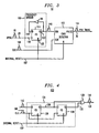
- FIG. 1 illustrates a demodulator 10 for demodulating a communications signal 18.
- the demodulator 10 comprises a synchronizer 12 for providing a transition signal 144 representing reference edges of the communication signal 18; a period-window detector 20 coupled to the synchronizer 12, for measuring a time interval between reference edges based on the transition signal 144; and a logic device 22 having logic inputs 24 coupled to the outputs of the period-window detector 20 and yielding a logic output signal 26 indicative of the presence or absence of a phase shift in the communications signal.
- the foregoing components of the demodulator 10 are well-suited for fabrication using conventional commercially available digital logic circuitry or programmable digital logic circuitry.
- the synchronizer 12 includes a synchronizer input 28 for accepting a communications signal 18 and a synchronizer output 30 for providing a transition signal 144 representing reference edges of the communications signal 18.
- a period-window detector 20 is coupled to the synchronizer 12 for receiving the transition signal 144.
- the period-window detector 20 measures a time interval between reference edges based on the transition signal 144.
- the period-window detector 20 has output signals indicative of durational states of the measured time interval.
- a logic device 22 has logic inputs 24 coupled to the outputs of the period-window detector 20.
- the logic device 22 yields a logic output signal 26 indicative of the presence or absence of a phase shift in the communications signal 18.
- the communications signal 18 includes a phase-shift modulated state and a generally unmodulated carrier state.
- the communications signal 18 optimally is a phase-shift-keying signal (PSK) such as a binary phase-shift-keying (BPSK) signal.
- PSK phase-shift-keying signal
- BPSK binary phase-shift-keying
- the demodulator 10 is well-suited for demodulating binary phase-shift-keying (BPSK) signals, although the demodulator 10 may operate on other PSK modulation schemes or variants of PSK modulation schemes.
- the demodulator 10 further preferably comprises a phase shift toggle circuit 32 connected to the logic device 22 and a carrier boundary detector 34 connected to the phase shift toggle circuit 32.
- the phase shift toggle circuit 32, the logic device 22, and the carrier boundary detector 34 may be readily fabricated using well-known digital logic integrated circuits or components.
- the phase shift toggle circuit 32 is adapted to receive the transition signal 144 and the logic output signal 26.
- the phase shift toggle circuit 32 provides demodulated data 38 at a toggle output 36.
- the carrier boundary detector 34 is adapted to detect the unmodulated carrier state and control the enablement of the toggle output 36 based upon the communications signal 18 being in the phase-shift modulated state or the unmodulated carrier state.
- the carrier boundary detector 34 has a clear carrier flip-flop input 308 for resetting the carrier boundary detector 34.
- the carrier boundary detector 34 accepts a carrier present input signal 44 from the phase shift toggle circuit 32 and provides an enable output signal 40 to the phase shift toggle circuit 32.
- the carrier present input signal 44 has a logic state indicative of the presence or absence of an unmodulated state (i.e. carrier only state).
- the enable output signal 40 provides a logic state generally indicative of the presence or absence of a message interval 52, an end portion of a leading carrier interval 50, and a beginning portion of a trailing carrier interval 54.
- the demodulator 10 may be manufactured using only minimal discrete components and basic printed circuit board (PCB) techniques, wherein the synchronizer 12, the period-window detector 20, the logic device 22, the carrier boundary detector 34, and the phase shift toggle circuit 32 may be embodied as field-programmable gate array elements.
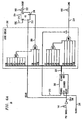
- FIG. 2A through FIG. 2E show the timing relationship between various waveforms associated with the demodulator 10, including the enable output signal 40 (Fig. 2A), carrier steady-state signal 42 (Fig. 2B), carrier present signal 44 (Fig. 2C), communications signal 18 (Fig. 2D), and demodulated data 38 (Fig. 2E).
- the dashed lines indicate the synchronization of the signals between different figures of FIG. 2A through FIG. 2E.
- the horizontal axis represents a common time axis for FIG. 2A through FIG. 2E, while each of the vertical axes represents signal amplitude in one corresponding figure.
- a typical PSK-modulated communications signal 18 is illustratively corrupted by noise during an inter-message noise interval 51 between adjacent message intervals 52.
- Inter-message noise refers to unwanted electromagnetic energy present between PSK message intervals 52.
- Inter-message noise may be modeled as a randomly occurring electromagnetic energy, within a frequency range affecting the communication signal 18, with an amplitude characterized by a probability density function.
- the demodulated data 38 is shown including a leading carrier interval 50, a message body 52, and a trailing carrier interval 54 without the unwanted effects of inter-message noise 51 in accordance with the demodulator 10.
- the synchronizer 12 preferably comprises a frequency divider 100 cooperatively coupled to an edge detector 102.
- the edge detector 102 accepts a reference clock signal 108.
- the synchronizer 12 includes a synchronizer input 28 for accepting a communications signal 18 and a synchronizer output 30 for transmitting a transition signal 144 to the period window detector 20.
- An internal reset input 107 is preferably provided for the synchronizer 12 and to edge detector 102.
- the frequency divider 100 divides the original frequency of the communications signal 18 (i.e. PSK modulated signal) to yield a divided frequency for the edge detector 102.
- the divisor is preferably two, although other configurations may use other positive integers.
- the frequency divider 100 generally comprises a digital logic circuit for dividing a radio frequency signal, such as the communications signal 18.
- the frequency divider 100 preferably includes a flip-flop 114 arranged in a toggling mode.
- the flip-flop 114 comprises a D-type flip-flop which includes a D input 116, an edge-triggered input 118, an active low reset input 120, and a Q output 122.
- a D-type flip-flop is described herein, any type of flip-flop or logic storage device capable of a toggling mode may be used to make the frequency divider 100.
- the Q output 122 is first inverted by an inverter 99 and then coupled as feedback to the D input 116. Therefore, a divided output signal 142 at the Q output 122 toggles at one-half the frequency of the D input 116.
- the edge detector 102 generally comprises a digital logic circuit for providing a timing relationship between transitions in a radio frequency signal, such as the communications signal 18.
- FIG. 4 shows an illustrative embodiment of the edge detector 102, in detail, in which the edge detector 102 includes a shift register 124 in combination with a exclusive "OR" gate 126.
- the divided output signal 142 of the D-type flip-flop 114 and a clock output signal 108 are coupled to the shift register 124.
- the shift register 124 may comprise two flip-flops 128 cascaded in the manner shown in FIG. 4.
- the Q outputs 130 of the cascaded flip-flops 128 are preferably exclusively OR'ed such that an output of an exclusive OR gate 126 provides a transition signal 144.
- the output of the exclusive OR gate 126 represents a pulse output 133 of the edge detector 102.
- the edge detector 102 includes an internal reset terminal 107 for resetting the edge detector 102.
- FIG. 5A depicts the communications signal 18 that is being applied to the synchronizer 12.
- the frequency divider 100 of synchronizer 12 divides the signal to obtain a divided signal 142 as shown in FIG. 5B, having a leading edge 138 and a trailing edge 140.
- the edge detector 102 of synchronizer 12 provides the transition signal 144 shown in FIG. 5C.
- the transition signal 144 preferably comprises a series of pulses 146 in which each pulse coincides with a reference edge, either a leading edge 138 or trailing edge 140 of divided signal 142, of the communications signal 18 after frequency division by the frequency divider 100.
- FIG. 5B shows the divided signal 142 designated as PSKDIV2.
- the divided signal 142 is applied as an input to the edge detector 102.
- the output waveform from the exclusive OR gate 126 of the edge detector 102 at pulse output 133 is the transition signal 144 and is designated PSK_TRANS in FIG. 5C.
- FIG. 5C shows the time between the pulses 146, which is called the pulse transition interval 148.
- the pulse transition interval 148 will generally vary with the instantaneous state of modulation of the communications signal.
- the horizontal axis represents a common time axis for FIG. 5A through FIG. 5C.
- Each vertical axis in FIG. 5A through FIG. 5C shows the logic state of a signal in one corresponding figure.
- the period-window detector 20 generally comprises a digital logic circuit for comparing input timing information on a communications signal 18 to a reference period-window to determine the presence or absence of phase shift in the communications signal 18.
- the period-window detector 20 preferably comprises a counter 200 operatively connected to a logic circuit 202 and a flip-flop 204 operatively connected to the logic circuit 202.
- the counter 200 has a clock input 206, a counter input 208 (or reset input) for accepting the transition signal 144, an enable input 210 receiving a feedback signal from the logic circuit 202, and a counter output 220 coupled to the logic circuit 202.
- the transition signal 144 is inverted prior to application to the counter 200.
- the flip-flop 204 has an edge-triggered input 212 which is coupled to the inverted transition signal. Another input 216 of the flip-flop 204, illustratively designated as a D input for a D-type flip-flop 204, is fixed at a fixed logic state (i.e. high logic level). A reset input 218 of the flip-flop 204 is coupled to an output 209 of the logic circuit 202. The flip-flop 204 has a first output indicative of one of the durational states. The logic circuit 202 has a second output 224 which may be indicative of another one of the states.
- the logic circuit 202 may be made from an arrangement of various multi-input logic gates, including NOR, NAND, AND, OR, or exclusive NOR gates.
- the illustrative example shown in FIG. 6A shows illustrative pin-outs between the logic gates and the counter 200.
- the counter 200 comprises at least an 11-bit counter to generate a time window to determine if the intervals between successive transition pulses of the transition signal are short pulse intervals, normal pulse intervals, or long pulse intervals.
- Short pulse intervals and long pulse intervals represent phase shift in the communications signal 18 associated with the modulated state.
- Normal pulse intervals represent no phase shift in the communications signal 18 associated with the unmodulated state. Normal pulse intervals are arranged to fall within the predetermined window width of the period window detector 20.
- the time window of the counter 200 may readily be changed via software instructions from a CPU to accommodate demodulation of communication signals 18 having different frequencies, phase shift or phase distortion characteristics.
- the transition signal 144 sets the flip-flop 204 and resets the counter 200 which then proceeds to count. If no new transition pulse 146 arrives before the counter 200 reaches a first minimum predetermined threshold time, then the flip-flop 204 is reset and the first output 222 (i.e. short) goes to a logic state (i.e. logic low) indicating that the period window detector 20 has not detected a short pulse interval, in the transition signal 144, as the durational state.
- the second output 224 (i.e. long) goes to a second logic state (i.e. high logic state) indicative of a long transition pulse as the durational state.
- a high logic state at the second output 224 disables the counter 200 so that the count is held until the next transition signal 144 arrives, both clearing and enabling the counter 200 for a new counting sequence.
- the transition pulse 144 arrives such that both the first output 222 and the second output 224 are simultaneously low during the arrival.
- the first minimum predetermined threshold time and the second minimum predetermined threshold time are selected based upon the frequency tolerance of the clock (i.e. CLK) of the demodulator 10, the distribution of measurements caused by jitter, and the frequency tolerance of the carrier derived from the modulator.
- CLK clock
- One illustrative source of jitter is a comparator which may be used to provide digitized PSK modulated data as input to the demodulator.
- an illustrative transition signal 144 at an input to a period-window detector 20 is temporally related to short and long output signals at a first output 222 and a second output 224, respectively.
- the signals in FIG. 6B through FIG. 6D are plotted with amplitudes of each signal on separate vertical axes and a common time scale on the horizontal axis. While the illustrative transition signal 144 shows pulses 146 in a particular sequence of a long pulse interval 601, a short pulse interval 602, and a normal pulse interval 603; the short, normal and long pulse intervals may occur in any order and any type of interval may occur with any frequency.
- the logic states of the short output signal 608 and the long output signal 610 indicate whether or not the communications signal 18 has been phase-shifted or modulated.
- the relative logic states of the transition signal 144, the short output signal 608, and the long output signal 610 may be expressed as a truth table in which the following states are present: (1) The short output signal 608 may be low and the long output signal 610 may be low for normal pulse intervals 603 - indicating no phase shift. (2) The short output signal 608 may be low and the long output signal 610 may be high for long pulse intervals 601 - indicating phase shift. (3) The short output signal 608 may be high and the long output 610 may be low for short pulse intervals 602 - indicating phase shift. Nevertheless, a period-window detector 20 falling within the scope of this invention may be practiced by using other logic states and truth table relationships not expressly set forth herein.
- the logic device 22 generally comprises a digital logic circuit for evaluating input logic states in accordance with a predetermined logic relationship or rule, and for providing a digital output consistent with the relationship or rule.
- the logic device 22 shown in FIG. 1 preferably comprises an OR gate or an equivalent logic circuit.
- the logic device 22 may comprise any logic structure or circuit capable of acting upon the durational states received from the period-window detector 20 to yield output information on the modulation of the communications signal 18.
- the logic device 22 has its inputs connected to the first output 222 and the second output 224 of the period-window detector 20.
- the first output 222 of the period-window detector 20 represents a phase change of the communications signal 18 as manifested by a measured time interval less than a minimum predetermined threshold time.
- the second output 224 of the period window detector 20 represents a phase change of the communications signal 18 as manifested by a measured time interval being greater than a maximum predetermined threshold time.
- the minimum and the maximum predetermined threshold times are proportional to stability factors and tolerance associated with a carrier frequency of the communications signal 18.
- the second output 224 disables the counter 200 if the measured time interval is greater than a maximum predetermined threshold time.
- first output 222 and the second output 224 may be replaced by a single output representing two possible states: a modulated state (i.e. phase-shifted) and an unmodulated state.
- the logic output 26 of the logic device 22 is preferably low.
- the logic output 26 may be high, indicating a phase shifted waveform.
- a demodulated data output or toggle output 36 of the demodulator 10 is activated and ripe for reading or further processing.
- the carrier boundary detector 34 generally comprises a digital logic circuit for evaluating a communications signal 18 to distinguish a message interval 52 from an inter-message noise interval 51.
- the carrier boundary detector 34 preferably comprises a carrier duration timer 300 operatively connected to a logic storage device.
- the logic storage device preferably comprises a flip-flop 302, although in alternate embodiments the logic storage device may comprise a latch, a memory device, or, a register, for example.
- the carrier boundary detector 34 has a clock input 304, a carrier present input 306, a clear carrier flip-flop input 308, and an enabling output 310.
- the carrier present input 306 is preferably inverted prior to application to the reset input of the timer 300.
- One of the timer outputs 318 of the carrier duration timer 300 is preferably coupled to an enable input 312 of the carrier duration timer 300 via an inverter 314.
- the toggle flip-flop 302 has an edge-triggered input 316 coupled to a timer output 318 of a timer, a logic input 320 labeled TE which is tied to a high logic state, a reset input 322 , and a Q output 310.
- the clear carrier flip-flop input 308 is connected to the reset input 322 of the flip-flop 302.
- the Q output 310 provides the enable output signal 40.
- a typical PSK modulated communications signal 18 may be corrupted by noise during an inter-message noise interval 51 (FIG. 2D) between messages.
- the noise in the inter-message noise interval 51 has a sufficient amplitude to negatively impact the performance of a demodulator without the beneficial action of the carrier boundary detector 34.
- the carrier boundary detector 34 eliminates, compensates for, suppresses, or otherwise reduces the deleterious effects of the inter-message noise 51 upon the demodulated output data during times between message intervals 52. Because the carrier boundary detector 34 functions as a noise eliminator, added attenuation for noise reduction purposes is rendered superfluous and the demodulator 10 is more responsive over a greater dynamic range of sensitivities than previously thought possible.
- a typical PSK modulated message during the message interval is preceded and followed by an unmodulated interval.
- the carrier boundary detector 34 discriminates between a modulated state (i.e. mode) and an unmodulated state (i.e. mode) of the communications signal 18.
- the unmodulated state of the communications signal 18 may be merely a generally square wave without intentional phase shifting.
- the unmodulated state preferably includes a leading carrier interval 50, which precedes the modulated state for a first fixed predetermined duration and a trailing carrier interval 54 which follows the modulated state for a second fixed predetermined duration.
- the leading carrier interval 50 and the trailing carrier interval 54 are preferably used for synchronization purposes to synchronize the decoding of modulated data in the message interval 52.
- the expiration of the first fixed predetermined duration indicates the imminent arrival time of the data or message body of the modulated state within the message interval 52.
- the expiration of the second fixed predetermined duration indicates the imminent arrival time of potential inter-message noise 51 between adjacent message intervals 52.
- the first fixed predetermined duration and the second predetermined fixed duration may range from approximately 200 to 1,000 unmodulated cycles of the communication signal 18, although other ranges are possible for practicing the invention.
- the carrier frequency boundary detector 34 initiates the carrier duration timer 300 having a starting time coincident with the beginning of the leading carrier interval 50 to prepare for reading the message body of the communications signal 18 in the modulated state upon the expiration of the timer 300.
- the carrier frequency boundary detector 34 also initiates the carrier duration timer 300 having a starting time coincident with a beginning of the trailing carrier interval 54 to prepare for temporarily disabling the demodulated output (i.e. toggle output 36) upon the expiration of the carrier duration timer 300.
- the temporarily disabling of the demodulated output between the expiration of the second predetermined duration and a start of a new first predetermined duration minimizes disruptive noise signals, which might otherwise be interpreted as corrupt data.
- the carrier signal present signal 44 remains low and the timer 300 is not held in reset. If no phase shifts are detected for the first fixed predetermined duration, the timer feedback bit of the carrier duration timer 300 goes high and toggles the enable output signal of the flip-flop 302 high, which in turn enables the demodulated PSK output of the demodulator 10. The feedback bit going high disables the carrier duration timer 300 from further counting. When the message body is being received, phase shifts repeatedly reset the carrier duration timer 300 so the feedback bit stays low.
- the clear carrier flip-flop input 308 may be pulsed low by a central processing unit (i.e. CPU) at a time between messages to guarantee that the enable output signal is low before the leading carrier tone is detected.
- a central processing unit i.e. CPU
- a noise eliminator comprises the carrier boundary detector 34.
- the noise eliminator discriminates between a message interval 52 and an inter-message noise interval 51 of the communications signal by recognizing a trailing carrier interval 54 and a leading carrier interval 50 as temporal boundaries of the inter-message noise interval 51.
- the noise eliminator is adapted to generate an eliminator output for indicating whether or not the logic output signal 26 of the logic device 22 is usable or potentially corrupt by noise in the inter-message noise interval 51.
- the noise eliminator preferably comprises a carrier duration timer 300 for synchronizing the trailing and leading carrier intervals with the noise eliminator output, which may be represented as enable output signal 40.
- the demodulator output or toggle output 36 may be coupled to the noise eliminator output so that the eliminator output controls enablement of the demodulator output.
- the phase shift toggle circuit generally comprises digital logic circuitry for providing a demodulated data output based upon timing information on transitions in a communications signal 18 and logic input indicative of the present or absence of a phase shift in the communications signal 18.
- the phase shift toggle circuit 32 preferably comprises a first flip-flop 400 cascaded with a second flip-flop 402.
- the first flip flop 400 has an edge-triggered input or strobe input for receiving the transition signal 144.
- the first flip flop 400 is arranged such that the data present on its input lines 404 just before a reference edge of the clock signal determines the output state of the first flip-flop 400 after the clock has pulsed.
- the second flip-flop 402 preferably comprises a T-type flip-flop arranged in a toggling mode to yield a demodulated data signal 38 at the demodulated signal output or toggle output 36.
- the first output 222 or the second output 224 of the logic device 22 will be high at the rising edge or a reference edge of the transition signal.
- the high logic level is latched into the first flip-flop 400.
- the rising edge then clocks the input to the second flip flop 402 to toggle the toggle output 36.
- the carrier present signal 44 has a high logic level if the previous PSK period was either a short pulse interval or a long pulse interval.
- the carrier present signal 44 then goes to the carrier boundary detector 34 and is used as described in the previous section.
- the demodulator 10 is primarily intended to yield demodulated data 38 at the toggle output 36 (i.e. demodulator output) from a PSK-modulated signal 18, a PSK-modulated signal, or a variant of a PSK-modulated signal, presented at the synchronizer input 28 (i.e. demodulator input).
- FIG. 9 illustrates an application of the demodulator 10 of the invention in a receiving system 500.
- the demodulator 10 is connected to the output 506 of digitizing comparator 508.
- the digitizing comparator 508 accepts raw phase shifted modulated data 504 from an analog receiver 502 and converts the signal in a suitable digital logic level signals in a PSK data format for the demodulator 10.
- the inputs to the demodulator 10 include the synchronizer input 28, a clock signal input 516, and a clear carrier flip-flop signal input 308.
- the synchronizer input 28 receives a PSK-modulated signal 18 from the comparator 508.
- the output 36 includes demodulated data which is preferably coupled to a central processing unit 512, such as a general purpose computer that feeds the clear carrier flip-flop signal input 308 to the demodulator 10.
- the demodulator 10 may be flexibly used in a prodigious assortment of specific applications, such as being used in a receiving system 500, by merely changing software configurable features.
- the demodulator 10 is preferably designed so as to be field configurable by using field programmable gate array (FPGA) technology to embody the demodulator components.
- FPGA field programmable gate array
- An FPGA-based demodulator may have a lower production cost than fixed-function demodulators if the FPGA demodulator is suited to a sufficiently large common pool of applications to meet manufacturing target volumes.
- an FPGA demodulator may be programmed to account for drift of a carrier frequency or a different carrier frequency entirely by changing a window width and a window center of a period window, which is associated with a period window detector 20 of the invention.
- the demodulator 10 of the present invention features a period-window detector 20 for establishing period-width windowing of a communications signal and a carrier boundary detector 34 for framing by carrier signal integration.
- the demodulator 10 of the present invention may be implemented with only minimal discrete components and basic printed circuit board (PCB) layouts.
- the carrier boundary detector 34 of the demodulator frames messages in a manner compatible with taking RSSI measurements over a wider dynamic range than demodulators using added attenuation.
- the demodulator 10 is well-suited for use in communications systems that carry Personal Communication Services (PCS) over coaxial cable or hybrid networks.
- the demodulator 10 may be used to demodulate status messages sent from a Cable Microcell Integrator (CMI), a hub site, a primary trunk, a switch point, a secondary trunk, or a subscriber device.
- CMS Cable Microcell Integrator
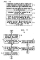
- FIG. 10 is a flow chart illustrating a preferred method of demodulating a phase-shift keyed communications signal with a demodulator 10 having a logic device 22.
- the demodulator is synchronized with a communications signal by generating a transition signal representing reference edges of the communications signal.
- a time interval between the reference edges of the communications signal is measured.
- a durational state associated with the measured time interval is established.
- the durational state is applied to a logic device to yield a logic output signal indicating the presence or absence of a phase shift in the communications signal.
- a demodulator output of the demodulator is controlled based upon whether the phase shift is present or absent such that the demodulator output is active if the phase shift is present and otherwise inactive to reduce intermessage noise associated with communication signal.
- Measuring the time interval in step S2 may further comprise measuring the time between successive transition signal pulses of the transition signal to establish the time interval.
- Controlling the output of the demodulator in step S5 may further comprise detecting an unmodulated carrier state and controlling an output of the demodulator based upon whether the communications signal is in an unmodulated state or a modulated state.
- the demodulator may be muted for a portion of the unmodulated state to minimize noise degradation of the received communication signal.
- FIG. 11 shows an illustrative example of step S3 in more detail than FIG. 10.
- a minimum predetermined threshold time and a maximum predetermined threshold time are set to define a time window for the period-window detector.
- the time window represents a time range which is proportional to a carrier frequency of the communications signal.
- step S6 the phase shift may be detected where the time interval previously measured in step S2 is less than a minimum predetermined threshold time set in step S16. If the measured time interval in step S6 is less than the minimum predetermined threshold, then a first durational state indicating phase shift is established in step S9 and the method continues at step S4. However, if the time interval previously measured in step S2 is greater than or equal to the minimum predetermined threshold set in step S16, then the method continues with step S7. In step S7, the phase shift may be detected where the time interval previously measured in step S2 is greater than a maximum predetermined threshold time set in step S16.
- step S10 a second durational state indicating a phase shift is established, and the method continues at step S4. Finally, if the measured time interval falls within the window between the minimum predetermined threshold and the maximum predetermined threshold previously set in S16, a third durational state indicating no phase shift is established in step S8 and the method continues at step S4.
- controlling the demodulator output in step S5 may include the step S11 of timing a first fixed predetermined duration corresponding to a duration of a leading carrier interval preceding the modulated mode to identify an imminent arrival time of a message body to prepare for enabling of a demodulator output of the demodulator.
- step S12 the demodulator is then enabled upon the expiration of the first predetermined duration. If the demodulator is enabled in step S12, demodulated output data is generated from the logic output signal and the time interval in step S15.
- a second fixed predetermined duration corresponding to a duration of a trailing carrier interval is timed in step S13.
- the trailing carrier interval follows the modulated mode.
- the demodulator is disabled upon the expiration of the second predetermined duration in step S14.
- the disabling of the demodulator output in step S14 upon expiration of the second predetermined duration reduces the effects of noise associated with the communications signal.
- the demodulator output is preferably only temporarily disabled such that the output is reactivated for subsequent messages upon the expiration of the first predetermined duration.
Landscapes
- Engineering & Computer Science (AREA)
- Computer Networks & Wireless Communication (AREA)
- Signal Processing (AREA)
- Digital Transmission Methods That Use Modulated Carrier Waves (AREA)
Claims (24)
- Démodulateur (10) pour démoduler un signal de communication à modulation par déplacement de phase (18) comprenant :un synchroniseur (12) pour accepter le signal de communication et sortir un signal de transition (144) représentant des bords de référence du signal de communication ; etun détecteur de fenêtre de période (20) couplé au synchroniseur et recevant le signal de transition, le détecteur de fenêtre de période mesurant un intervalle de temps entre les bords de référence du signal de communication sur la base du signal de transition et fournissant des sorties révélatrices d'états de durée de l'intervalle de temps mesuré ; etun dispositif logique (22), ayant des entrées logiques (24) couplées aux sorties du détecteur de fenêtre de période, produisant un signal de sortie logique (26) révélateur de la présence ou l'absence d'un déplacement de phase dans le signal de communication ; etcaractérisé par :un éliminateur de bruit (34) pour discriminer entre un intervalle de message (52) et un intervalle de bruit inter-messages (51) du signal de communication par la reconnaissance d'un intervalle de porteuse arrière (54) et d'un intervalle de porteuse avant (50) en tant que frontières temporelles de l'intervalle de bruit inter-messages, l'éliminateur de bruit étant apte à générer une sortie d'éliminateur pour indiquer si le signal de sortie logique est utilisable ou non ou est potentiellement altéré par un bruit dans l'intervalle de bruit inter-messages.
- Démodulateur selon la revendication 1 dans lequel le signal de communication comprend un état modulé par déplacement de phase et un état de porteuse généralement non modulé, le démodulateur étant en outre caractérisé par :un circuit à bascule par déplacement de phase (32) pour recevoir le signal de transition et le signal de sortie logique et fournir des données démodulées à une sortie de bascule ; etun détecteur de frontière de porteuse (34) pour détecter l'état de porteuse non modulé du signal de communication et commander l'activation de la sortie de bascule sur la base du signal de communication étant soit dans l'état modulé par déplacement de phase, soit dans l'état non modulé.
- Démodulateur selon la revendication 2 dans lequel le détecteur de frontière de porteuse active la sortie de bascule lorsque que le signal de communication est dans l'état modulé par déplacement de phase.
- Démodulateur selon la revendication 1 caractérisé en outre par un circuit à bascule par déplacement de phase (32) pour recevoir le signal de transition et le signal de sortie logique et fournir des données démodulées à une sortie de bascule, l'éliminateur de bruit activant la sortie de bascule alors que le signal de sortie logique indique la présence du déplacement de phase.
- Démodulateur selon la revendication 1 dans lequel l'éliminateur de bruit comprend un temporisateur de durée de porteuse pour synchroniser les intervalles de porteuse arrière et avant avec la sortie d'éliminateur.
- Démodulateur selon la revendication 1 caractérisé en outre par une sortie de démodulateur couplée à la sortie d'éliminateur de bruit, la sortie d'éliminateur de bruit commandant l'activation de la sortie de démodulateur.
- Démodulateur selon la revendication 1 dans lequel le détecteur de fenêtre de période comprend un compteur (200), un circuit logique (202) et une bascule bistable (204), le compteur ayant une entrée de compteur (208) pour accepter le signal de transition et ayant une sortie de compteur (220) couplée au circuit logique, la bascule bistable ayant une première sortie révélatrice de l'un des états de durée, et le circuit logique ayant une seconde sortie (224) révélatrice d'un autre des états de durée.
- Démodulateur selon la revendication 7 dans lequel la première sortie du circuit logique représente un changement de phase du signal de communication tel que manifesté par un intervalle de temps mesuré inférieur à un temps de seuil prédéterminé minimum, le temps de seuil prédéterminé minimum étant proportionnel à une fréquence porteuse du signal de communication.
- Démodulateur selon la revendication 7 dans lequel la seconde sortie du circuit logique représente un changement de phase du signal de communication tel que manifesté par un intervalle de temps mesuré étant supérieur à un temps de seuil prédéterminé maximum, le temps de seuil prédéterminé maximum étant basé sur une fréquence porteuse du signal de communication.
- Démodulateur selon la revendication 7 dans lequel la seconde sortie du circuit logique inactive le compteur si l'intervalle de temps mesuré est supérieur à un temps de seuil prédéterminé maximum.
- Démodulateur selon la revendication 1 dans lequel le signal de transition représente un intervalle de temps entre des bords avant du signal de communication, et dans lequel le synchroniseur divise le signal de communication par un entier positif constant pour déduire le signal de transition.
- Démodulateur selon la revendication 1 dans lequel le synchroniseur, le détecteur de fenêtre de période et le dispositif logique comprennent des éléments de réseau prédiffusé programmable par l'utilisateur.
- Démodulateur selon la revendication 1 dans lequel le dispositif logique comprend une porte « OU ».
- Démodulateur selon la revendication 1 dans lequel le signal de communication comprend un mode modulé par déplacement de phase et un état de porteuse généralement non modulé, le démodulateur comprenant en outre un détecteur de frontière de porteuse pour détecter au moins un desdits modes pour supprimer un bruit en dehors du mode modulé par déplacement de phase.
- Démodulateur selon la revendication 14 dans lequel le détecteur de frontière de porteuse comprend un temporisateur de durée de porteuse (300) et un dispositif de stockage logique couplé audit temporisateur de durée de porteuse, le dispositif de stockage logique ayant une sortie verrouillable pour activer ou inactiver une sortie du démodulateur.
- Démodulateur selon la revendication 15 dans lequel le temporisateur a une première durée prédéterminée fixée correspondant à une durée d'un intervalle de porteuse avant précédant le mode modulé et une seconde durée prédéterminée fixée correspondant à une durée d'un intervalle de porteuse arrière suivant le mode modulé, et dans lequel le détecteur de frontière de porteuse inactive la sortie du démodulateur à l'expiration de la seconde durée prédéterminée fixée pour réduire les effets d'un bruit associé au signal de communication.
- Démodulateur selon la revendication 1, dans lequel
le démodulateur est un démodulateur de réseau prédiffusé programmable par l'utilisateur (FPGA) ; et
le signal de communication est un signal à modulation par déplacement de phase (PSK) ; et
le signal de transition sorti par le synchroniseur comprend une série d'impulsions générée en réponse à des bords de référence du signal PSK ; et
l'intervalle de temps mesuré provient des bords de référence du signal PSK qui correspondent à des impulsions successives parmi les impulsions générées, le détecteur de fenêtre de période ayant une pluralité de sorties révélatrice d'un déplacement de phase potentiel dans le signal PSK sur la base de l'intervalle de temps mesuré ; et
le démodulateur est en outre caractérisé par un circuit à bascule par déplacement de phase fournissant une sortie de données démodulées, le circuit à bascule par déplacement de phase étant apte à recevoir le signal de transition provenant du synchroniseur et apte à changer la sortie de données démodulées d'un premier état à un second état si l'intervalle de temps se situe dans une période de fenêtre prédéterminée pendant une durée fixée prédéterminée ; et
Le démodulateur est en outre caractérisé par un détecteur de frontière de porteuse pour détecter un début et une fin du message et fournir une sortie pour inactiver la sortie de données démodulées après la détection d'un signal de porteuse non modulé arrière après la fin. - Procédé de démodulation d'un signal de communication modulé par déplacement de phase avec un démodulateur ayant un dispositif logique, le procédé comprenant les étapes de :synchronisation du démodulateur avec le signal de communication par la génération d'un signal de transition modulé pour représenter des bords de référence du signal de communication ;mesure d'un intervalle de temps entre les bords de référence du signal de communication ;établissement d'un état de durée associé à l'intervalle de temps mesuré ; application de l'état de durée au dispositif logique pour produire un signal de sortie logique indiquant la présence ou l'absence d'un déplacement de phase dans le signal de communication ; et le procédé est caractérisé par :la discrimination entre un intervalle de message et un intervalle de bruit inter-messages du signal de communication par la reconnaissance d'un intervalle de porteuse arrière et d'un intervalle de porteuse avant en tant que frontières temporelles de l'intervalle de bruit inter-messages.
- Procédé selon la revendication 18 caractérisé en outre par l'étape de détection d'un état de porteuse non modulé du signal de communication et de commande d'une sortie du démodulateur sur la base du signal de communication étant soit dans un état de porteuse non modulé, soit dans un état modulé.
- Procédé selon la revendication 18 caractérisé en outre par l'étape de :temporisation d'une première durée prédéterminée fixée correspondant à une durée de l'intervalle de porteuse avant précédant un mode modulé du signal de communication pour identifier un temps d'arrivée imminente d'un corps de message afin de préparer l'activation d'une sortie du démodulateur.
- Procédé selon la revendication 18 caractérisé en outre par l'étape de :temporisation d'une seconde durée prédéterminée fixée correspondant à une durée de l'intervalle de porteuse arrière suivant le mode modulé du signal de communication ; etinactivation d'une sortie du démodulateur à l'expiration de la seconde durée prédéterminée pour réduire les effets d'un bruit associé au signal de communication.
- Procédé selon la revendication 18 dans lequel l'étape de mesure comprend en outre :le calcul du temps entre des impulsions successives de signal de transition du signal de transition pour établir l'intervalle de temps.
- Procédé selon la revendication 18 caractérisé en outre par l'étape de :détection d'un changement de phase du signal de communication manifesté par un intervalle de temps mesuré inférieur à un temps de seuil prédéterminé minimum, le temps de seuil prédéterminé étant proportionnel à une fréquence porteuse du signal de communication.
- Procédé selon la revendication 18 caractérisé en outre par l'étape de :détection d'un changement de phase du signal de communication manifesté par un intervalle de temps mesuré supérieur à un temps de seuil prédéterminé maximum, le temps de seuil prédéterminé étant proportionnel à une fréquence porteuse du signal de communication.
Applications Claiming Priority (2)
| Application Number | Priority Date | Filing Date | Title |
|---|---|---|---|
| US09/181,810 US6341146B1 (en) | 1998-10-29 | 1998-10-29 | Phase-shift-keying demodulator and demodulation method using a period-width windowing technique |
| US181810 | 1998-10-29 |
Publications (3)
| Publication Number | Publication Date |
|---|---|
| EP0998084A2 EP0998084A2 (fr) | 2000-05-03 |
| EP0998084A3 EP0998084A3 (fr) | 2003-10-08 |
| EP0998084B1 true EP0998084B1 (fr) | 2007-02-07 |
Family
ID=22665904
Family Applications (1)
| Application Number | Title | Priority Date | Filing Date |
|---|---|---|---|
| EP99308181A Expired - Lifetime EP0998084B1 (fr) | 1998-10-29 | 1999-10-18 | Démodulateur et procédé de démodulation de signaux MDP qui employent une technique de fenêtrage de la largeur de la période |
Country Status (9)
| Country | Link |
|---|---|
| US (1) | US6341146B1 (fr) |
| EP (1) | EP0998084B1 (fr) |
| JP (1) | JP3659476B2 (fr) |
| KR (1) | KR20000047572A (fr) |
| CN (1) | CN1253443A (fr) |
| AU (1) | AU5597999A (fr) |
| BR (1) | BR9905875A (fr) |
| CA (1) | CA2284138A1 (fr) |
| DE (1) | DE69935055T2 (fr) |
Families Citing this family (11)
| Publication number | Priority date | Publication date | Assignee | Title |
|---|---|---|---|---|
| JP2001267897A (ja) * | 2000-03-17 | 2001-09-28 | Oki Electric Ind Co Ltd | 遅延装置および方法 |
| US6944565B2 (en) * | 2003-08-08 | 2005-09-13 | Poseidon Scientific Instruments Pty Ltd | Signal analysis instrument, and a module for a signal analysis instrument |
| AU2003231682B2 (en) * | 2003-08-08 | 2009-04-23 | Poseidon Scientific Instruments Pty Ltd | A Signal Analysis Instrument, And a Module For A Signal Analysis Instrument |
| KR100976625B1 (ko) * | 2008-10-15 | 2010-08-18 | 한국전자통신연구원 | 타임투디지털컨버터를 이용한 위상 편이 복조기 |
| TWI413384B (zh) * | 2008-10-28 | 2013-10-21 | Univ Nat Central | Low complexity and low power consumption of the keyed phase shifter system |
| WO2010070459A1 (fr) * | 2008-12-16 | 2010-06-24 | Acceleradio Ltd. | Système et procédé d'exploitation d'un dispositif de relais |
| US7911266B2 (en) * | 2009-01-19 | 2011-03-22 | National Central University | Low complexity and low power phase shift keying demodulator structure |
| CN101692662A (zh) * | 2009-09-03 | 2010-04-07 | 中国石油大学(华东) | 一种相位调制方法、设备以及系统 |
| US9014303B2 (en) * | 2010-03-25 | 2015-04-21 | Custom Link Corporation | Receiver apparatus and method for carrier state modulation |
| KR102298160B1 (ko) * | 2015-08-13 | 2021-09-03 | 삼성전자주식회사 | 반도체 장치 및 이를 포함하는 통신 시스템 |
| JP6716485B2 (ja) * | 2017-03-24 | 2020-07-01 | 日立オートモティブシステムズ株式会社 | 回転角度検出装置 |
Family Cites Families (4)
| Publication number | Priority date | Publication date | Assignee | Title |
|---|---|---|---|---|
| JP2771354B2 (ja) * | 1991-08-26 | 1998-07-02 | 日本電気株式会社 | 復調器 |
| DE69329960T2 (de) * | 1992-05-29 | 2001-06-13 | Sony Corp., Tokio/Tokyo | Demodulator für phasensprungmodulierte (PSK) Signale |
| US5757868A (en) * | 1994-02-16 | 1998-05-26 | Motorola, Inc. | Digital phase detector with integrated phase detection |
| US5533069A (en) * | 1994-10-26 | 1996-07-02 | International Business Machines Corporation | Method and apparatus for digital frequency compensation of carrier drift in a PSK demodulator |
-
1998
- 1998-10-29 US US09/181,810 patent/US6341146B1/en not_active Expired - Lifetime
-
1999
- 1999-09-28 CA CA002284138A patent/CA2284138A1/fr not_active Abandoned
- 1999-10-18 DE DE69935055T patent/DE69935055T2/de not_active Expired - Lifetime
- 1999-10-18 EP EP99308181A patent/EP0998084B1/fr not_active Expired - Lifetime
- 1999-10-20 AU AU55979/99A patent/AU5597999A/en not_active Abandoned
- 1999-10-22 BR BR9905875-8A patent/BR9905875A/pt not_active Application Discontinuation
- 1999-10-27 CN CN99123171A patent/CN1253443A/zh active Pending
- 1999-10-29 JP JP30788599A patent/JP3659476B2/ja not_active Expired - Fee Related
- 1999-10-29 KR KR1019990047521A patent/KR20000047572A/ko not_active Withdrawn
Also Published As
| Publication number | Publication date |
|---|---|
| JP3659476B2 (ja) | 2005-06-15 |
| EP0998084A2 (fr) | 2000-05-03 |
| AU5597999A (en) | 2000-05-04 |
| CA2284138A1 (fr) | 2000-04-29 |
| DE69935055D1 (de) | 2007-03-22 |
| DE69935055T2 (de) | 2007-07-19 |
| JP2000151733A (ja) | 2000-05-30 |
| BR9905875A (pt) | 2000-09-05 |
| KR20000047572A (ko) | 2000-07-25 |
| US6341146B1 (en) | 2002-01-22 |
| CN1253443A (zh) | 2000-05-17 |
| EP0998084A3 (fr) | 2003-10-08 |
Similar Documents
| Publication | Publication Date | Title |
|---|---|---|
| US6008746A (en) | Method and apparatus for decoding noisy, intermittent data, such as manchester encoded data or the like | |
| US4450573A (en) | Bit data operated squelch | |
| EP0998084B1 (fr) | Démodulateur et procédé de démodulation de signaux MDP qui employent une technique de fenêtrage de la largeur de la période | |
| US4457005A (en) | Digital coherent PSK demodulator and detector | |
| WO1997032416A1 (fr) | Boucle numerique a phase verrouillee et systeme de recuperation d'horloge numerique | |
| US5311556A (en) | Digital FSK transmitter receiver and method of operating same | |
| EP0709993B1 (fr) | Démodulation de phase, par la mesure du temp entre passages par zéro | |
| EP0258697B1 (fr) | Démodulateur de signal FSK | |
| KR100431716B1 (ko) | 지연 동기 루프를 이용한 디지털 주파수 편이 복조기 및복조 방법 | |
| CA1228124A (fr) | Circuit de detection d'interferences pour recepteur radio | |
| JPH06507769A (ja) | クロック同期方法および回路 | |
| CA1189911A (fr) | Blocage pilote par les donnees relatives aux porteuses | |
| EP0709990B1 (fr) | Procédé et dispositif de détection numérique de porteuse dans un réseau local sans fils | |
| US20030094974A1 (en) | Clock's out-of-synchronism state detection circuit and optical receiving device using the same | |
| JP3003981B2 (ja) | ディジタル高周波信号における搬送波ドリフトを補償するための方法及び装置 | |
| JP3344530B2 (ja) | デジタル信号伝送方法およびデジタル信号復調装置 | |
| JP2703676B2 (ja) | ディジタルダイバーシチ装置 | |
| KR0176139B1 (ko) | 비트 동기회로 | |
| JP3622887B2 (ja) | 受信機 | |
| JPH05260017A (ja) | スペクトル拡散通信方式並びに送信回路及び受信回路 | |
| JP3551096B2 (ja) | デジタル信号処理装置 | |
| JP2000295193A (ja) | 同期検出装置 | |
| JP2000022576A (ja) | 周波数ずれ監視回路 | |
| JPH07118708B2 (ja) | バースト信号位相制御回路 | |
| JPS6335039A (ja) | Pll同期検出回路 |
Legal Events
| Date | Code | Title | Description |
|---|---|---|---|
| PUAI | Public reference made under article 153(3) epc to a published international application that has entered the european phase |
Free format text: ORIGINAL CODE: 0009012 |
|
| AK | Designated contracting states |
Kind code of ref document: A2 Designated state(s): AT BE CH CY DE DK ES FI FR GB GR IE IT LI LU MC NL PT SE |
|
| AX | Request for extension of the european patent |
Free format text: AL;LT;LV;MK;RO;SI |
|
| PUAL | Search report despatched |
Free format text: ORIGINAL CODE: 0009013 |
|
| AK | Designated contracting states |
Kind code of ref document: A3 Designated state(s): AT BE CH CY DE DK ES FI FR GB GR IE IT LI LU MC NL PT SE |
|
| AX | Request for extension of the european patent |
Extension state: AL LT LV MK RO SI |
|
| 17P | Request for examination filed |
Effective date: 20040327 |
|
| AKX | Designation fees paid |
Designated state(s): DE FR GB |
|
| GRAP | Despatch of communication of intention to grant a patent |
Free format text: ORIGINAL CODE: EPIDOSNIGR1 |
|
| GRAS | Grant fee paid |
Free format text: ORIGINAL CODE: EPIDOSNIGR3 |
|
| GRAA | (expected) grant |
Free format text: ORIGINAL CODE: 0009210 |
|
| AK | Designated contracting states |
Kind code of ref document: B1 Designated state(s): DE FR GB |
|
| REG | Reference to a national code |
Ref country code: GB Ref legal event code: FG4D |
|
| REF | Corresponds to: |
Ref document number: 69935055 Country of ref document: DE Date of ref document: 20070322 Kind code of ref document: P |
|
| ET | Fr: translation filed | ||
| PLBE | No opposition filed within time limit |
Free format text: ORIGINAL CODE: 0009261 |
|
| STAA | Information on the status of an ep patent application or granted ep patent |
Free format text: STATUS: NO OPPOSITION FILED WITHIN TIME LIMIT |
|
| 26N | No opposition filed |
Effective date: 20071108 |
|
| REG | Reference to a national code |
Ref country code: GB Ref legal event code: 732E Free format text: REGISTERED BETWEEN 20131107 AND 20131113 |
|
| REG | Reference to a national code |
Ref country code: FR Ref legal event code: CD Owner name: ALCATEL-LUCENT USA INC. Effective date: 20131122 |
|
| REG | Reference to a national code |
Ref country code: FR Ref legal event code: GC Effective date: 20140410 |
|
| REG | Reference to a national code |
Ref country code: FR Ref legal event code: RG Effective date: 20141015 |
|
| REG | Reference to a national code |
Ref country code: FR Ref legal event code: PLFP Year of fee payment: 17 |
|
| REG | Reference to a national code |
Ref country code: FR Ref legal event code: PLFP Year of fee payment: 18 |
|
| PGFP | Annual fee paid to national office [announced via postgrant information from national office to epo] |
Ref country code: DE Payment date: 20161020 Year of fee payment: 18 Ref country code: GB Payment date: 20161020 Year of fee payment: 18 Ref country code: FR Payment date: 20161020 Year of fee payment: 18 |
|
| REG | Reference to a national code |
Ref country code: DE Ref legal event code: R119 Ref document number: 69935055 Country of ref document: DE |
|
| GBPC | Gb: european patent ceased through non-payment of renewal fee |
Effective date: 20171018 |
|
| REG | Reference to a national code |
Ref country code: FR Ref legal event code: ST Effective date: 20180629 |
|
| PG25 | Lapsed in a contracting state [announced via postgrant information from national office to epo] |
Ref country code: GB Free format text: LAPSE BECAUSE OF NON-PAYMENT OF DUE FEES Effective date: 20171018 Ref country code: DE Free format text: LAPSE BECAUSE OF NON-PAYMENT OF DUE FEES Effective date: 20180501 |
|
| PG25 | Lapsed in a contracting state [announced via postgrant information from national office to epo] |
Ref country code: FR Free format text: LAPSE BECAUSE OF NON-PAYMENT OF DUE FEES Effective date: 20171031 |
|
| REG | Reference to a national code |
Ref country code: DE Ref legal event code: R081 Ref document number: 69935055 Country of ref document: DE Owner name: WSOU INVESTMENTS, LLC, LOS ANGELES, US Free format text: FORMER OWNER: LUCENT TECHNOLOGIES INC., MURRAY HILL, N.J., US |