EP0999517A1 - Transpondeur actif rechargeable - Google Patents
Transpondeur actif rechargeable Download PDFInfo
- Publication number
- EP0999517A1 EP0999517A1 EP98120833A EP98120833A EP0999517A1 EP 0999517 A1 EP0999517 A1 EP 0999517A1 EP 98120833 A EP98120833 A EP 98120833A EP 98120833 A EP98120833 A EP 98120833A EP 0999517 A1 EP0999517 A1 EP 0999517A1
- Authority
- EP
- European Patent Office
- Prior art keywords
- transponder
- voltage
- supply
- accumulator
- current
- Prior art date
- Legal status (The legal status is an assumption and is not a legal conclusion. Google has not performed a legal analysis and makes no representation as to the accuracy of the status listed.)
- Granted
Links
Images



Classifications
-
- G—PHYSICS
- G06—COMPUTING OR CALCULATING; COUNTING
- G06K—GRAPHICAL DATA READING; PRESENTATION OF DATA; RECORD CARRIERS; HANDLING RECORD CARRIERS
- G06K19/00—Record carriers for use with machines and with at least a part designed to carry digital markings
- G06K19/06—Record carriers for use with machines and with at least a part designed to carry digital markings characterised by the kind of the digital marking, e.g. shape, nature, code
- G06K19/067—Record carriers with conductive marks, printed circuits or semiconductor circuit elements, e.g. credit or identity cards also with resonating or responding marks without active components
- G06K19/07—Record carriers with conductive marks, printed circuits or semiconductor circuit elements, e.g. credit or identity cards also with resonating or responding marks without active components with integrated circuit chips
- G06K19/0701—Record carriers with conductive marks, printed circuits or semiconductor circuit elements, e.g. credit or identity cards also with resonating or responding marks without active components with integrated circuit chips at least one of the integrated circuit chips comprising an arrangement for power management
- G06K19/0702—Record carriers with conductive marks, printed circuits or semiconductor circuit elements, e.g. credit or identity cards also with resonating or responding marks without active components with integrated circuit chips at least one of the integrated circuit chips comprising an arrangement for power management the arrangement including a battery
-
- G—PHYSICS
- G06—COMPUTING OR CALCULATING; COUNTING
- G06K—GRAPHICAL DATA READING; PRESENTATION OF DATA; RECORD CARRIERS; HANDLING RECORD CARRIERS
- G06K19/00—Record carriers for use with machines and with at least a part designed to carry digital markings
- G06K19/06—Record carriers for use with machines and with at least a part designed to carry digital markings characterised by the kind of the digital marking, e.g. shape, nature, code
- G06K19/067—Record carriers with conductive marks, printed circuits or semiconductor circuit elements, e.g. credit or identity cards also with resonating or responding marks without active components
- G06K19/07—Record carriers with conductive marks, printed circuits or semiconductor circuit elements, e.g. credit or identity cards also with resonating or responding marks without active components with integrated circuit chips
- G06K19/0701—Record carriers with conductive marks, printed circuits or semiconductor circuit elements, e.g. credit or identity cards also with resonating or responding marks without active components with integrated circuit chips at least one of the integrated circuit chips comprising an arrangement for power management
-
- G—PHYSICS
- G06—COMPUTING OR CALCULATING; COUNTING
- G06K—GRAPHICAL DATA READING; PRESENTATION OF DATA; RECORD CARRIERS; HANDLING RECORD CARRIERS
- G06K19/00—Record carriers for use with machines and with at least a part designed to carry digital markings
- G06K19/06—Record carriers for use with machines and with at least a part designed to carry digital markings characterised by the kind of the digital marking, e.g. shape, nature, code
- G06K19/067—Record carriers with conductive marks, printed circuits or semiconductor circuit elements, e.g. credit or identity cards also with resonating or responding marks without active components
- G06K19/07—Record carriers with conductive marks, printed circuits or semiconductor circuit elements, e.g. credit or identity cards also with resonating or responding marks without active components with integrated circuit chips
- G06K19/0723—Record carriers with conductive marks, printed circuits or semiconductor circuit elements, e.g. credit or identity cards also with resonating or responding marks without active components with integrated circuit chips the record carrier comprising an arrangement for non-contact communication, e.g. wireless communication circuits on transponder cards, non-contact smart cards or RFIDs
Definitions
- the present invention relates to the field of active transponders and, more specifically, active transponders switchable into passive transponders.
- Such a portable device contains data which can be transferred, in the form of radio signals between a base station stationary serving as a transceiver and this device.
- a base station stationary serving as a transceiver
- transponders there are conventionally two types of transponders: passive transponders and active transponders.
- a passive transponder is arranged to convert a radio signal from a base station, in an electrical voltage which then supplies the power necessary for the operation of the transponder.
- Such a passive transponder includes an antenna arranged to receive and transmit signals containing data, a capacitor storage connected to the antenna, to be able to store the electrical energy received by the antenna, and a circuit integrated connected to the antenna and to the capacitor storage, to be able to process the data received by the antenna, and provide the latter with other data to transmit as a radio signal.
- the storage capacitor realizes, in such transponder, supply of electrical power of the integrated circuit.
- An active transponder is arranged to transmit data over large distances on the order of several hundreds of meters. Indeed, remote interrogation of such an active transponder does not require a low distance between the base station and this transponder, since there is no transfer of energy from the base station to the transponder.
- FIG. 1 shows such an active transponder designated by reference 1.
- This transponder includes a antenna 3 arranged to be able to receive and transmit radio signals 4 containing data, one integrated circuit 5 connected to the antenna 3, to be able process data received by antenna 3, and provide the latter other data to be sent in the form of radio signal.
- Active transponder 1 includes in addition a battery 7 capable of supplying power to different components of the transponder 1.
- a disadvantage of the active transponder 1 is that it operates normally, as long as battery 7 provides sufficient electrical voltage to supply the assembly components of the transponder 1. In case this the latter is incorporated in a vehicle door key, as soon as battery 7 no longer provides a voltage level sufficient to ensure the proper functioning of the transponder 1, the latter no longer provides the door opening control, which is generally troublesome for the vehicle user.
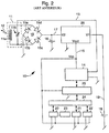
- FIG. 2 of this description shows a dual transponder 10 which includes an antenna circuit 11, a modulation-demodulation circuit 14, a rectifier 15, a storage capacitor 16, a battery 18, a central processing unit 20, a ROM memory 21, RAM memory 22, clock system 23 and a switching circuit 26.
- the antenna circuit 11 is arranged to receive and transmit data to and from an external device, in the form of a radiofrequency wave 12.
- the antenna circuit 11 comprises an antenna 11a formed by a coil and a capacitor 11b.
- the modulation-demodulation circuit 14 is arranged to modulate a digital signal received from a command 25 into an analog signal, and to demodulate a analog signal received through the antenna 11a into a digital signal.
- Reference 13 designates a line by which a received signal is transferred from the antenna 11a to the modulation-demodulation circuit 14, and by which a signal to be transmitted is transferred from modulation-demodulation circuit 3 at the antenna 11a.
- the rectifier circuit 15 is formed by a diode bridge 15a to 15d to convert an alternating voltage of the wave radio frequency 12 received by the antenna 11a in a voltage continues V2.
- the storage capacitor 16 is arranged to store the rectified DC voltage V2, this the latter being intended to be supplied to the various components via a connection line 17.
- the central processing unit 20 is arranged to process data according to an execution program.
- the ROM 21 read only memory (acronym from English "Read-Only Memory”) is arranged to store the program of execution.
- RAM 22 (acronym from English “Random-Access Memory”) is arranged to store temporarily data.
- the clock system 23 is arranged to supply a clock signal in response to which the processing unit 20 operates.
- Reference 24 designates a bus through which data is transmitted and addresses.
- the battery 18 is arranged to supply a voltage electric V1 intended to supply the various components of the transponder 10, via a connection line 19. Note that the voltage of operation of the transponder 10 is of the order of 5 V.
- the switching circuit 26 is connected to the lines 19 and 17, and is arranged so that when the voltage V2 present across the storage capacitor 16 is higher than voltage V1, transponder 10 operates using the electrical power supplied by the storage capacitor 16, via the line 17, and that, when the voltage V2 is lower than the voltage V1, the transponder 10 operates using the electric power supplied by battery 1, by via line 19.
- a disadvantage of the transponder 10 lies in the after the battery 18 has been discharged, the power supply of the transponder components 10 can only be supplied by the capacitor of storage 16. In the case where the transponder 10 is incorporated into a vehicle door key, this transponder should be a short distance from the base station so as to receive from the base station bases sufficient energy for its operation. Other says, once the battery 18 is discharged, the user of the key must wait the time necessary for the charge of the capacitor 18, before identification can have place, which can be particularly unpleasant for this user.
- An object of the present invention is to provide a dual transponder overcomes the disadvantages of conventional active transponders, in particular a transponder active to maintain a power level sufficient to ensure its functioning.
- Another object of the present invention is to provide an active transponder that meets the criteria traditional in the semiconductor industry, complexity and cost.
- the subject of the invention is an active transponder comprising in particular first and second means for compare the first and second signals respectively supply at a minimum threshold provided by a first means of supply and, in response, provide respectively first and second control signals and means for load controlled by the first and second signals of control, and arranged so that when the first and second power signals are respectively below and above the minimum threshold, the accumulator is charged, via the charging means, to from the energy contained in the storage medium.
- An advantage of such an arrangement of the charging means and of the first and second means of comparison is to order a charge of the accumulator, as soon as the first supply voltage becomes internal to minimum threshold.
- the minimum threshold corresponds to minimum level of supply voltage required for perform all of the transponder's functions, which has the advantage of providing the transponder with power sufficient to perform all of the functions of this transponder.
- Another advantage of comparing the first supply voltage at such a minimum threshold is to avoid the battery does not discharge completely during operation, which avoids putting the means of short circuit treatment.
- the first means of comparison can compare the first supply voltage to a maximum threshold which represents the upper limit of the battery charge, which has the advantage of avoiding overcharging the battery.
- the processing means is arranged to receive electrical energy from the storage medium when charging the accumulator, and the accumulator, once loaded.
- FIG. 3 represents a first embodiment preferred of the active transponder according to the present invention, designated by reference 30.
- the transponder 30 includes an antenna 32, a means 36, an accumulator 38 and a means of storage 40.
- the antenna 32 is arranged to be able to receive and transmit data to and from an external device (for example a conventional base station), in the form of a radiofrequency signal 34.
- an external device for example a conventional base station
- antenna 32 using a connected coil between two connection terminals 320 and 321, as is known per se.
- the processing means 36 further comprises two connection terminals 360 and 361 connected respectively at terminals 320 and 321 of antenna 32.
- the means of treatment 36 is arranged to be able to receive antenna 32 the data received, process this data, and provide antenna 32 with identification data to transmit in the form of a radio frequency signal.
- the processing means 36 comprises a logic block may include a central processing unit (not shown in Figure 3), a storage means (not shown in Figure 3), and a clock system (not shown in Figure 3).
- said processing unit is produced central, said storage means and said system clock like the components described in relation with figure 2.
- the processing means 36 is also arranged for ability to convert radio frequency signal 34 to power source capable of supplying voltage continues V2. To this end, the processing means 36 includes an interface including a circuit modulation-demodulation (not shown in Figure 3), a rectification circuit (not shown in Figure 3) and a terminal 364 connected to the storage means 40.
- said circuit is produced. modulation-demodulation and said rectification circuit at like the components described in relation to the figure 2.
- the means of storage 40 by forming a capacitor comprising a terminal 400 connected to terminal 364 of the processing means 36, and a ground terminal 401 connected to the ground of the transponder 30, so that the voltage between terminals 400 and 401 is equal to the DC voltage V2.
- the storage means 40 may contain an electrical charge equivalent to a voltage in the range of 2 to 6 V.
- the processing means 36 includes a ground terminal 362 connected to the ground of the transponder 10, and a terminal supply 363 intended to receive a voltage supply V1 supplied by the accumulator 38.
- the accumulator 38 is arranged to be able to provide the supply voltage V1, the latter to be sufficient to power all of the components of the transponder 30.
- the accumulator 38 includes a supply terminal 380 for supplying the voltage V1, and a ground terminal 381 connected to ground of the transponder 30.
- the accumulator 38 is arranged to be able to provide the supply voltage V1, the latter to be sufficient to power all of the components of the transponder 30.
- the accumulator 38 includes a supply terminal 380 for supplying the voltage V1, and a ground terminal 381 connected to ground of the transponder 30.
- a conventional accumulator Preferably, one realizes the accumulator 38 using a conventional accumulator.
- the transponder 30 further comprises two means of comparison 42 and 46, and a charging means 50.
- the comparison means 42 is arranged to be able to compare the electric voltage V1 supplied by the accumulator at a predetermined minimum voltage threshold Vmin and, in response, supply an electrical voltage V3 of so that when the voltage V1 is below the threshold Vmin, the voltage V3 is equal to a voltage level "0" and that, when the voltage V1 is greater than the threshold Vmin, the voltage V3 is equal to a voltage level "1".
- the comparison means 42 comprises a first input terminal 420 connected to a means of supply 44, to receive the threshold Vmin, and a second input terminal 421 connected to terminal 380 of the accumulator 38, to receive the voltage V1.
- the way comparator 42 also includes an output terminal 422, to supply the voltage V3 containing the result of the comparison between the voltage V1 and the threshold Vmin.
- the output terminal 422 of the comparison means 42 is connected to the charging means 50, as described below.
- the comparison means 42 is preferably carried out using an operational amplifier, as is known per se.
- the supply means 44 comprises a terminal output 440 connected to terminal 420 by means of comparison 42, to provide the threshold Vmin, as well as a supply terminal and a ground terminal, the latter not being shown in Figure 3.
- the means of supply 44 is arranged so that the threshold value Vmin is sufficient to meet criteria predetermined correct functioning of the transponder 30, i.e. to determine if the voltage value supplied by the accumulator is sufficient to power transponder 30, i.e. to ensure carrying out all the functions of the transponder 30.
- the supply means 44 are preferably produced by using a conventional reference voltage source.
- the means of comparison 46 is arranged to be able to compare at the threshold Vmin the electric voltage V2 present at terminals 400 and 401 of the storage means 40 and, in response, providing a electrical voltage V4 so that when the voltage V2 is below the threshold Vmin, the voltage V4 is equal to the voltage level "0" and that, when the voltage V2 is greater than the threshold Vmin, the voltage V4 is equal to the voltage level "1".
- the comparison means 46 comprises a first input terminal 460 connected to terminal 440 of the supply means 44, to receive the threshold Vmin, and a second input terminal 461 connected to terminal 400 of the storage means 40, for receiving the voltage V2.
- the comparison means 46 also includes a terminal output 462, to supply the electrical voltage V4 containing the result of the comparison between the voltage V2 and the threshold Vmin.
- the output terminal 462 of the means of comparison 46 is connected to charging means 50, as this is described below.
- the comparison means 15 is preferably carried out using an operational amplifier, as is known per se.
- the charging means 50 is arranged to be able to charge the accumulator 38 from the energy stored in the storage means 40 (i.e. from the voltage V2), in response to the comparisons of voltages V1 and V2 at threshold Vmin (that is to say in response to the voltages V3 and V4).
- the charging means 50 comprises a first input terminal 500 connected to terminal 400 of the storage means 40, for receiving the voltage V2, and second and third input terminals 501 and 502 connected respectively to the output terminals 422 and 462, to receive the respective voltages V3 and V4.
- the way charging station 50 also includes an output terminal 503 connected to terminal 380 of accumulator 38, by which the charging of the accumulator 38 takes place, like this is described below.
- FIG. 4 shows in detail the means of load 50 of the active transponder 30 of FIG. 3.
- the charging means 50 includes a current mirror 52 which can supply by the terminal 503 a load current I1, a current source 54 being able to supply a first reference current I2, a first switch 56 connected to terminal 501, so to be able to be controlled by the voltage V3, and a second switch 58 connected to terminal 502, so that can be controlled by voltage V4.
- the current mirror 52 is connected to terminal 500, through switch 58, so that the voltage V2 serves as supply voltage for the mirror current 52.
- the current mirror 52 is also connected to the current source 54, via the switch 56, so the current I2 can be copied by the current mirror 52 in the form of current I1.
- the current mirror 52 is produced at from two field effect transistors T1 and T2, as is known per se.
- the source current 54 from a current mirror formed of two field effect transistors T3 and T4, this mirror receiving a second reference current Iref supplied by a temperature stabilized current source (not shown in Figure 4).
- the switches 56 and 58 forming two respectively T5 and T6 field effect transistors controlled by the voltages V3 and V4, respectively.
- the transistors T1, T2, T5 and T6 each have a P-type channel
- the transistors T3 and T4 each have an N-type channel.
- an advantage of the arrangement charging means 50 and comparison means 42 and 46 in transponder 30 is to order a load of the accumulator 38, as soon as the voltage V1 supplied by this last becomes less than the threshold Vmin, that is to say from that the accumulator 38 can no longer provide a sufficient power supply to the transponder 30.
- the active transponder 30 has the advantage of ability to automatically recharge battery 38 as soon as that the latter is no longer sufficiently charged to ensure all functions of the transponder 30.
- all of the components of the transponder 30 are produced, by forming an integrated structure by steps of manufacturing a die of CMOS type known per se.
- CMOS type known per se.
- a monolithic manner is carried out in a single semiconductor substrate, the processing means 36, storage means 40, the s mean s of comparison 42 and 46, as well as load means 50.
- figures 5 and 7 represent two active transponders 60 and 70, respectively.
- the structures of transponders 60 and 70 are close to that of transponder 30.
- the objects of transponders 60 and 70 identical to those described in relationship with Figure 3 have been designated by the same references.
- the transponder 60 further includes switching means 62 and means additional supply 63, these components being connected to comparison means 42 to form a double threshold comparator, in order to avoid an overload of the accumulator 38, as described below.
- the supply means 63 comprises a terminal output 630 connected to switching means 62, for provide a maximum voltage threshold Vmax, as well as a supply terminal and a ground terminal, the latter not being shown in Figure 5.
- the means of supply 63 is arranged so that the threshold value Vmax represents the upper limit of the load of accumulator 38.
- the means of supply 63 using a voltage source of reference stable in temperature.
- the switching means 62 is arranged to be able to providing the comparison means 42 with a threshold Vth which is equal knows at threshold Vmin, i.e. at threshold Vmax, depending of the result of the comparison of the voltage V1.
- the switching means 62 comprises two input terminals 620 and 621 connected respectively to the terminal 630 of supply means 63 and terminal 440 of supply means, to receive the threshold respectively maximum Vmax and the minimum threshold Vmin.
- Way to switching 62 further includes a control terminal 622 connected to terminal 422 of comparison means 42, for receive the voltage V3, and an output terminal 623 connected to terminal 420 of comparison means 42, for provide the threshold Vth.
- the switching means 62 are preferably produced using two conventional transmission doors.
- FIG. 6 represents a curve 65 illustrating the relation between the voltage V1 supplied by the accumulator 38 and the voltage V3 supplied by the comparison means 42, this curve comprising six segments "A" to "F".
- the transponder 60 forms an improvement of the transponder 30 of FIG. 3, since the transponder 60 takes into account the upper load limit of the accumulator 38, which advantageously achieves a safety for the integrity of this accumulator.
- the processing means 36 further comprises two input terminals 365 and 366 connected respectively to the output terminal 422 of the comparison means 42 and at the output terminal 462 of the comparison means 46, and a output terminal 367 connected to terminals 501 and 502 of the charging medium 50.
- the processing means 36 of FIG. 7 is programmed so as to be able to supply, via the terminal 367, a control voltage V5 by means of load 50, in response to the electrical voltages V3 and V4 received by the respective bounds 365 and 366. It is noted that such a control of the charging means 50 is carried out so identical to the command described in relation to Figures 3 and 4.
- the control voltage V5 includes first and second bits containing states respective voltages V3 and V4.
- the processing means 36 can be arranged so that it can be connected: by means 40 by terminal 364, when charging the accumulator 38 (that is to say when the voltages V3 and V4 are equal to the respective levels "0" and "1"), of so that the electrical energy needed to power the transponder 70 is provided by the storage means 40; and to accumulator 38 via terminal 363, once accumulator 38 charged (i.e. when the voltage V3 is equal to level "1"), so that the energy necessary to power the transponder 70 is supplied by the accumulator 38.
- transponder 70 when charging accumulator 38, transponder 70 operates at like a passive transponder. Indeed, electrical power is then supplied by the means storage 40 which contains the energy received by the antenna 32, from the radiofrequency signal 34 emitted by said base station.
- FIGS. 4 to 6 we will describe the operation of the transponder 60, referring again to FIGS. 4 to 6 described above, and using figure 8 which represents four timing diagrams 81 to 84 illustrating the developments temporal voltages V1 to V4, respectively.
- time t1 corresponds to a moment from which the transponder 60 is located in the magnetic field of a transmitting base station data and energy in the form of the signal radio frequency 34.
- the antenna 32 of the transponder 60 receives in the form of the radiofrequency signal 34 of the data and of the energy.
- the storage means 40 receives said energy from antenna 32, via processing means 36, so that the voltage V2 increases until exceeding the threshold Vmin at an instant t2. he shows that, at time t2, the voltage V4 supplied by the comparison means 46 goes from level "0" to level "1". Beyond the instant t2, the voltage V2 continues to grow to a maximum level corresponding to the maximum load that the storage means 40 can store. Consequently, beyond the instant t2, the voltage V4 is equal to level "1".
- the transponder 60 receives also said data from antenna 32, and processes these data, which results in power consumption electric. This results in a drop in the level of voltage V1, from time t1. As long as the transponder 60 is located in said magnetic field, and works, the voltage level V1 continues to drop until reaching the threshold Vmin, at an instant t3.
- the voltage V1 continues to decrease and becomes below the threshold Vmin, while the voltage V2 is greater than the level Vmin.
- the voltage V3 goes from level "1" to level "0".
- the charging current I1 is supplied to accumulator 38, as already described above in relation to Figure 4.
- the charging means 50 is controlled to charge the accumulator 38. It there is an increase in voltage V1, and a drop in the voltage V2.
- the means of storage 40 provides energy through charging 50 to charge the accumulator 38 and that, on the other hand, it receives power from the base station, by through the antenna 32.
- the voltage V1 increases and reaches the threshold Vmax, which results in a passage of the voltage V3 from level "0" to level "1".
- the charge stored in the accumulator 38 is maximum, and the current source 54 of the charging means 50 is not no longer connected to the current mirror 52: the charge of the accumulator 38 by the charging means 50 is finished.
- the transponder according to the present invention can be advantageously used in a vehicle door key, which can remotely identify the key.
- the transponder 60 can operate under this application according to three different modes: “rest” mode, "identification” mode and “charge” mode.
Landscapes
- Engineering & Computer Science (AREA)
- Computer Hardware Design (AREA)
- Microelectronics & Electronic Packaging (AREA)
- Physics & Mathematics (AREA)
- General Physics & Mathematics (AREA)
- Theoretical Computer Science (AREA)
- Computer Networks & Wireless Communication (AREA)
- Near-Field Transmission Systems (AREA)
- Secondary Cells (AREA)
- Electrotherapy Devices (AREA)
Abstract
Description
- la figure 1 déjà citée représente un transpondeur actif classique;
- la figure 2 déjà citée représente un transpondeur dual classique;
- la figure 3 représente un premier mode de réalisation préféré du transpondeur actif selon la présente invention;
- la figure 4 représente de façon détaillée un composant du transpondeur actif de la figure 3;
- la figure 5 représente un deuxième mode de réalisation du transpondeur actif selon la présente invention;
- la figure 6 représente une courbe illustrant la relation entre deux tensions électriques présentes dans le transpondeur actif de la figure 5;
- la figure 7 représente un troisième mode de réalisation du transpondeur actif selon la présente invention; et
- la figure 8 représente un chronogramme d'une tension électrique présente dans le transpondeur actif de la figure 5.
Claims (12)
- Transpondeur actif (30; 60; 70) comprenant :une antenne (32) agencée pour pouvoir recevoir et émettre un signal radioélectrique (34) contenant des données;un moyen de traitement (36) connecté à ladite antenne, et agencé pour pouvoir fournir à ladite antenne des données d'identification à émettre sous forme de signal radioélectrique;un accumulateur (38) agencé pour pouvoir fournir un premier signal d'alimentation électrique (V1) aux composants dudit transpondeur; etun moyen de stockage (40) agencé pour pouvoir stocker de l'énergie électrique provenant dudit signal radioélectrique reçu par ladite antenne, et fournir un deuxième signal d'alimentation électrique (V2), ce transpondeur étant caractérisé en ce qu'il comprend en outre :des premier et deuxième moyens (42, 46) pour comparer respectivement lesdits premier et deuxième signaux d'alimentation à un seuil minimal (Vmin) fourni par un premier moyen de fourniture (44) et, en réponse, fournir respectivement des premier et deuxième signaux de commande (V3, V4); etun moyen de charge (50) commandé par lesdits premier et deuxième signaux de commande, et agencé de sorte que, lorsque lesdits premier et deuxième signaux d'alimentation sont respectivement inférieur et supérieur audit seuil minimal, ledit accumulateur est chargé, par l'intermédiaire dudit moyen de charge, à partir de l'énergie contenue dans ledit moyen de stockage.
- Transpondeur (30; 60; 70) selon la revendication 1, caractérisé en ce que ledit seuil minimal (Vmin) correspond au niveau minimal d'alimentation électrique nécessaire pour assurer l'ensemble des fonctions dudit transpondeur.
- Transpondeur (30; 60; 70) selon la revendication 1, caractérisé en ce que ledit moyen de charge (50) comprend un premier miroir de courant (52) pouvant fournir un courant de charge (I1), une source de courant (54) pouvant fournir un premier courant de référence (I2), des premier et deuxième commutateurs (56, 58) commandés respectivement par lesdits premier et deuxième signaux de commande (V3, V4), et en ce que ledit premier miroir de courant (52) est agencé pour pouvoir : être alimenté par ledit deuxième signal d'alimentation (V2), en fonction de l'état dudit premier commutateur; et être connecté à ladite source de courant (54), en fonction de l'état dudit deuxième commutateur, de sorte que, quand lesdits premier et deuxième commutateurs sont passants, ledit premier courant de référence est recopié par ledit premier miroir de courant sous la forme dudit courant de charge.
- Transpondeur (30; 60; 70) selon la revendication 3, caractérisé en ce que ledit premier miroir de courant (52) est formé de premier et deuxième transistors à effet de champ (T1, T2), en ce que ladite source de courant (54) est formée d'un deuxième miroir de courant comprenant des troisième et quatrième transistors à effet de champ (T3, T4), et recevant un deuxième courant de référence (Iref) fourni par une source de courant stabilisée en température, et en ce que lesdits premier et deuxième commutateurs (56, 58) sont formés respectivement de cinquième et sixième transistors a effet de champ (T5, T6) commandés par lesdits premier et deuxième signaux de commande (V3, V4), respectivement.
- Transpondeur (30; 60; 70) selon la revendication 4, caractérisé en ce que lesdits premier, deuxième, cinquième et sixième transistors à effet de champ (T1, T2, T5, T6) ont chacun un canal d'un premier type de conductivité (P), et en ce que lesdits troisième et quatrième transistors à effet de champ (T3, T4) ont chacun un canal d'un deuxième type de conductivité (N) différent dudit premier type de conductivité.
- Transpondeur (60) selon la revendication 1, caractérisé en ce qu'il comprend en outre un comparateur à double seuil comprenant : ledit premier moyen de comparaison (42) et un moyen de commutation (62) pouvant recevoir ledit premier signal de commande (V3) et, en réponse, fournir audit premier moyen de comparaison (42) un seuil (Vth) qui est égal soit audit seuil minimal (Vmin) soit à un seuil maximal (Vmax) fourni par un deuxième moyen de fourniture (63).
- Transpondeur (60) selon la revendication 6, caractérisé en ce que ledit seuil maximal (Vmax) représente la limite supérieure de la charge dudit accumulateur (38).
- Transpondeur (70) selon la revendication 1, caractérisé en ce que ledit moyen de traitement (36) est agencé pour pouvoir recevoir lesdits premier et deuxième signaux de commande (V3, V4) et, en réponse, fournir un troisième signal de commande (V5) pouvant entraíner la charge dudit accumulateur (38).
- Transpondeur (70) selon la revendication 8, caractérisé en ce que ledit moyen de traitement (36) est agencé pour recevoir l'énergie électrique nécessaire à alimenter ledit transpondeur : dudit moyen de stockage (40), lors de la charge dudit accumulateur (38); et dudit accumulateur 38, une fois que ce dernier est suffisamment chargé.
- Transpondeur actif (30; 60; 70) selon la revendication 1, caractérisé en ce que ledit moyen de traitement (36), ledit moyen de stockage (40), lesdits premier et deuxième moyens de comparaison (42, 46) et ledit moyen de charge (50) sont réalisés de façon monolithique dans un unique substrat semi-conducteur.
- Transpondeur actif (30 ; 60 ; 70) selon la revendication 10, caractérisé en ce que ladite antenne (32) est réalisée de façon monolithique dans ledit substrat.
- Dispositif portatif comprenant un transpondeur actif (30; 60; 70) selon l'une quelconque des revendications précédentes.
Priority Applications (5)
| Application Number | Priority Date | Filing Date | Title |
|---|---|---|---|
| EP98120833A EP0999517B1 (fr) | 1998-11-03 | 1998-11-03 | Transpondeur actif rechargeable |
| DE69815350T DE69815350T2 (de) | 1998-11-03 | 1998-11-03 | Wiederladbarer aktiver Transponder |
| AT98120833T ATE242517T1 (de) | 1998-11-03 | 1998-11-03 | Wiederladbarer aktiver transponder |
| US09/430,164 US6462647B1 (en) | 1998-11-03 | 1999-10-29 | Rechargeable active transponder |
| JP11314210A JP2000151460A (ja) | 1998-11-03 | 1999-11-04 | 充電式能動トランスポンダ |
Applications Claiming Priority (1)
| Application Number | Priority Date | Filing Date | Title |
|---|---|---|---|
| EP98120833A EP0999517B1 (fr) | 1998-11-03 | 1998-11-03 | Transpondeur actif rechargeable |
Publications (2)
| Publication Number | Publication Date |
|---|---|
| EP0999517A1 true EP0999517A1 (fr) | 2000-05-10 |
| EP0999517B1 EP0999517B1 (fr) | 2003-06-04 |
Family
ID=8232909
Family Applications (1)
| Application Number | Title | Priority Date | Filing Date |
|---|---|---|---|
| EP98120833A Expired - Lifetime EP0999517B1 (fr) | 1998-11-03 | 1998-11-03 | Transpondeur actif rechargeable |
Country Status (5)
| Country | Link |
|---|---|
| US (1) | US6462647B1 (fr) |
| EP (1) | EP0999517B1 (fr) |
| JP (1) | JP2000151460A (fr) |
| AT (1) | ATE242517T1 (fr) |
| DE (1) | DE69815350T2 (fr) |
Cited By (6)
| Publication number | Priority date | Publication date | Assignee | Title |
|---|---|---|---|---|
| WO2002071328A1 (fr) * | 2001-03-02 | 2002-09-12 | Schlumberger Systemes | Carte a puce avec alimentation en energie integree |
| WO2003091943A1 (fr) * | 2002-04-24 | 2003-11-06 | Marconi Intellectual Property (Us) Inc | Dispositif et procede de recharge d'une source d'energie |
| EP2114019A1 (fr) | 2008-04-30 | 2009-11-04 | STMicroelectronics (Rousset) SAS | Recharge d'un transpondeur actif |
| WO2010114576A1 (fr) * | 2009-03-30 | 2010-10-07 | Igt | Jeton de pari intelligent et techniques pour le pistage de jeton de pari |
| WO2010146277A1 (fr) | 2009-06-19 | 2010-12-23 | Stmicroelectronics (Rousset) Sas | Récupération d'énergie par un transpondeur électromagnétique |
| US8277314B2 (en) | 2006-11-10 | 2012-10-02 | Igt | Flat rate wager-based game play techniques for casino table game environments |
Families Citing this family (42)
| Publication number | Priority date | Publication date | Assignee | Title |
|---|---|---|---|---|
| US7248145B2 (en) | 2000-02-28 | 2007-07-24 | Magellan Technology Oty Limited | Radio frequency identification transponder |
| US7259654B2 (en) | 2000-02-28 | 2007-08-21 | Magellan Technology Pty Limited | Radio frequency identification transponder |
| GB2362070B (en) * | 2000-05-05 | 2004-06-16 | Nokia Mobile Phones Ltd | Communication devices and method of communication |
| GB0102882D0 (en) * | 2001-02-06 | 2001-03-21 | Koninkl Philips Electronics Nv | Signalling system and a transport for use in the system |
| US6944424B2 (en) * | 2001-07-23 | 2005-09-13 | Intermec Ip Corp. | RFID tag having combined battery and passive power source |
| US7565108B2 (en) * | 2002-03-26 | 2009-07-21 | Nokia Corporation | Radio frequency identification (RF-ID) based discovery for short range radio communication with reader device having transponder functionality |
| US6700491B2 (en) * | 2002-06-14 | 2004-03-02 | Sensormatic Electronics Corporation | Radio frequency identification tag with thin-film battery for antenna |
| US8905834B2 (en) | 2007-11-09 | 2014-12-09 | Igt | Transparent card display |
| US8795061B2 (en) | 2006-11-10 | 2014-08-05 | Igt | Automated data collection system for casino table game environments |
| EP1620956B1 (fr) * | 2003-04-29 | 2010-04-07 | Nxp B.V. | Circuit pour dispositif sans contact pourvu de modes d'envoi actif et passif |
| JP2007519268A (ja) * | 2003-06-25 | 2007-07-12 | コーニンクレッカ フィリップス エレクトロニクス エヌ ヴィ | 負荷期間を修正する修正手段を備えたデータキャリア |
| DE60330507D1 (de) * | 2003-07-22 | 2010-01-21 | Nokia Corp | Lesereinrichtung für einen hochfrequenz-identifikations-transponder mit transponder-funktionalität |
| US7176784B2 (en) * | 2004-01-21 | 2007-02-13 | Battelle Memorial Institute K1-53 | Multi-mode radio frequency device |
| WO2005081183A1 (fr) * | 2004-01-23 | 2005-09-01 | Nokia Corporation | Procede, dispositif et systeme destines a une fourniture automatisee de donnees selectives fondee sur des informations de contexte grace a des moyens d'identification |
| WO2005093643A1 (fr) | 2004-03-17 | 2005-10-06 | Nokia Corporation | Fourniture de donnees en continu par transpondeurs d'identification par radiofrequence |
| EP1725977B1 (fr) | 2004-03-19 | 2009-04-15 | Nokia Corporation | Dispositif d'identification logique detecteur et radio et procede d'amelioration du fonctionnement du terminal |
| DE502004009736D1 (de) * | 2004-04-01 | 2009-08-20 | Conti Temic Microelectronic | Verfahren und einrichtung zur übertragung zwischen einem steuergerät und einem radmodul |
| EP1738296B1 (fr) * | 2004-04-14 | 2008-02-27 | Matsushita Electric Industrial Co., Ltd. | Carte sans contact |
| JP4528332B2 (ja) * | 2005-02-09 | 2010-08-18 | エヌエックスピー ビー ヴィ | 無線移動通信機器の安全なnfc機能を確保する方法、及び安全なnfc機能を有する無線移動通信機器 |
| US7400250B2 (en) * | 2005-04-29 | 2008-07-15 | Nokia Corporation | Indicating radio frequency identification (RF-ID) tag |
| CN102360442B (zh) * | 2006-03-10 | 2015-01-07 | 株式会社半导体能源研究所 | 半导体器件及其操作方法 |
| EP2002383B1 (fr) | 2006-03-15 | 2012-04-25 | Semiconductor Energy Laboratory Co., Ltd. | Dispositif à semi-conducteurs |
| KR101435966B1 (ko) * | 2006-05-31 | 2014-08-29 | 가부시키가이샤 한도오따이 에네루기 켄큐쇼 | 반도체 장치 및 상기 반도체 장치를 가진 ic 라벨, ic 태그, 및 ic 카드 |
| US9489813B1 (en) * | 2006-09-22 | 2016-11-08 | Michael L. Beigel | System for location in environment and identification tag |
| JP5412034B2 (ja) | 2006-12-26 | 2014-02-12 | 株式会社半導体エネルギー研究所 | 半導体装置 |
| US7843316B1 (en) * | 2007-03-19 | 2010-11-30 | Synopsys, Inc. | Power-on reset apparatus, systems, and methods |
| DE102007027610A1 (de) * | 2007-06-12 | 2008-12-24 | Atmel Germany Gmbh | Transponder, Verfahren zum Betrieb eines Transponders |
| AU2009273748A1 (en) | 2008-07-21 | 2010-01-28 | Sato Holdings Corporation | A device having data storage |
| US8432070B2 (en) * | 2008-08-25 | 2013-04-30 | Qualcomm Incorporated | Passive receivers for wireless power transmission |
| US8947041B2 (en) | 2008-09-02 | 2015-02-03 | Qualcomm Incorporated | Bidirectional wireless power transmission |
| US8547227B2 (en) * | 2008-09-10 | 2013-10-01 | Avery Dennison Corporation | RF communication device with energy enhancement |
| US8532724B2 (en) | 2008-09-17 | 2013-09-10 | Qualcomm Incorporated | Transmitters for wireless power transmission |
| SI22945A (sl) * | 2008-12-16 | 2010-06-30 | IDS@d@o@o | Postopek za baterijsko in pasivno napajanje RFID nalepke in preklopno vezje za izvajanje tega postopka |
| EP2280580A1 (fr) * | 2009-07-07 | 2011-02-02 | Nokia Corporation | Transfert de données avec dispositifs de communication alimentés sans fil |
| JP4982594B2 (ja) * | 2009-12-25 | 2012-07-25 | 株式会社東芝 | 近距離無線通信装置 |
| DE102011100095B4 (de) * | 2011-04-29 | 2014-12-24 | Gottfried Wilhelm Leibniz Universität Hannover | Transpondereinheit |
| FR2976103B1 (fr) | 2011-06-03 | 2013-05-17 | St Microelectronics Rousset | Aide au positionnement d'un transpondeur |
| FR2976104B1 (fr) | 2011-06-03 | 2013-11-15 | St Microelectronics Rousset | Securisation d'une communication entre un transpondeur electromagnetique et un terminal |
| FR2976105B1 (fr) | 2011-06-03 | 2013-05-17 | St Microelectronics Rousset | Securisation d'une communication par un transpondeur electromagnetique |
| FR2976102B1 (fr) | 2011-06-03 | 2013-05-17 | St Microelectronics Rousset | Assistance au positionnement d'un transpondeur |
| US8818267B2 (en) | 2011-10-26 | 2014-08-26 | Qualcomm Incorporated | NFC transceiver utilizing common circuitry for active and passive modes |
| US9929779B2 (en) * | 2015-12-01 | 2018-03-27 | Maxim Integrated Products, Inc. | Power adaptive dual mode card emulation system for NFC and RFID application |
Citations (2)
| Publication number | Priority date | Publication date | Assignee | Title |
|---|---|---|---|---|
| US4962485A (en) * | 1988-02-16 | 1990-10-09 | Citizen Watch Co., Ltd. | Noncontacting IC card supplied with power from an outside source |
| GB2292866A (en) * | 1994-08-30 | 1996-03-06 | Mitsubishi Electric Corp | Power supply for non-contact IC card |
Family Cites Families (4)
| Publication number | Priority date | Publication date | Assignee | Title |
|---|---|---|---|---|
| US5483827A (en) * | 1994-06-03 | 1996-01-16 | Computer Methods Corporation | Active integrated circuit transponder and sensor apparatus for sensing and transmitting vehicle tire parameter data |
| US5850181A (en) * | 1996-04-03 | 1998-12-15 | International Business Machines Corporation | Method of transporting radio frequency power to energize radio frequency identification transponders |
| US5606323A (en) * | 1995-08-31 | 1997-02-25 | International Business Machines Corporation | Diode modulator for radio frequency transponder |
| US5822683A (en) * | 1996-04-05 | 1998-10-13 | Ball Aerospace And Technologies Corp. | Pseudo-passive transponder device |
-
1998
- 1998-11-03 AT AT98120833T patent/ATE242517T1/de not_active IP Right Cessation
- 1998-11-03 EP EP98120833A patent/EP0999517B1/fr not_active Expired - Lifetime
- 1998-11-03 DE DE69815350T patent/DE69815350T2/de not_active Expired - Lifetime
-
1999
- 1999-10-29 US US09/430,164 patent/US6462647B1/en not_active Expired - Lifetime
- 1999-11-04 JP JP11314210A patent/JP2000151460A/ja active Pending
Patent Citations (2)
| Publication number | Priority date | Publication date | Assignee | Title |
|---|---|---|---|---|
| US4962485A (en) * | 1988-02-16 | 1990-10-09 | Citizen Watch Co., Ltd. | Noncontacting IC card supplied with power from an outside source |
| GB2292866A (en) * | 1994-08-30 | 1996-03-06 | Mitsubishi Electric Corp | Power supply for non-contact IC card |
Cited By (6)
| Publication number | Priority date | Publication date | Assignee | Title |
|---|---|---|---|---|
| WO2002071328A1 (fr) * | 2001-03-02 | 2002-09-12 | Schlumberger Systemes | Carte a puce avec alimentation en energie integree |
| WO2003091943A1 (fr) * | 2002-04-24 | 2003-11-06 | Marconi Intellectual Property (Us) Inc | Dispositif et procede de recharge d'une source d'energie |
| US8277314B2 (en) | 2006-11-10 | 2012-10-02 | Igt | Flat rate wager-based game play techniques for casino table game environments |
| EP2114019A1 (fr) | 2008-04-30 | 2009-11-04 | STMicroelectronics (Rousset) SAS | Recharge d'un transpondeur actif |
| WO2010114576A1 (fr) * | 2009-03-30 | 2010-10-07 | Igt | Jeton de pari intelligent et techniques pour le pistage de jeton de pari |
| WO2010146277A1 (fr) | 2009-06-19 | 2010-12-23 | Stmicroelectronics (Rousset) Sas | Récupération d'énergie par un transpondeur électromagnétique |
Also Published As
| Publication number | Publication date |
|---|---|
| EP0999517B1 (fr) | 2003-06-04 |
| ATE242517T1 (de) | 2003-06-15 |
| DE69815350T2 (de) | 2004-04-29 |
| US6462647B1 (en) | 2002-10-08 |
| DE69815350D1 (de) | 2003-07-10 |
| JP2000151460A (ja) | 2000-05-30 |
Similar Documents
| Publication | Publication Date | Title |
|---|---|---|
| EP0999517B1 (fr) | Transpondeur actif rechargeable | |
| EP1617550B1 (fr) | Circuit d'alimentation adaptable | |
| FR2936886A1 (fr) | Dispositif electronique et gestion des communications sans contact concurrentes d'un tel dispositif et d'un equipement hote | |
| WO2002009028A1 (fr) | Transpondeur passif a faible consommation | |
| EP1936541B1 (fr) | Chargeur de batterie fonctionnant par "tout ou rien" avec circuit de protection d'alimentation pour circuits intégrés monolithiques utilisant l'énergie de l'antenne | |
| EP2507739A1 (fr) | Prolongateur d'antenne rfid auto-parametrable | |
| EP0926623A1 (fr) | Transpondeur actif commutable en transpondeur passif | |
| CA2657699A1 (fr) | Dispositif d'identification par radiofrequence (rfid) appose sur un objet a identifier | |
| FR2967538A1 (fr) | Procede pour moduler l'impedance d'un circuit d'antenne | |
| FR2707131A1 (fr) | Dispositif électronique comprenant un régulateur de charge interne pour contrôler l'application d'un courant de charge et procédé qui lui est associé. | |
| EP2810334B1 (fr) | Systeme de communication dans une batterie electrique | |
| EP1040447B1 (fr) | Transpondeur actif commutable en transpondeur passif | |
| FR2792137A1 (fr) | Detection, par un lecteur de transpondeur electromagnetique, de la distance qui le separe d'un transpondeur | |
| FR2782402A1 (fr) | Dispositif de controle d'acces entre une clef et une serrure electroniques | |
| FR3092706A1 (fr) | Dispositif de fourniture d'une puissance d'alimentation | |
| EP3831050A1 (fr) | Dispositif d'echantillonnage ameliore | |
| EP1087332A1 (fr) | Transpondeur destiné à plusieurs applications différentes | |
| EP0926855B1 (fr) | Transpondeur pour communication dite "half-duplex" | |
| FR3119058A1 (fr) | Gestion de la communication sans contact et du chargement sans contact à partir d’un dispositif sans contact, et dispositif sans contact correspondant | |
| WO2021094669A1 (fr) | Dispositif de communication optique sans fil | |
| EP1039652B1 (fr) | Arrangement d'antenne | |
| FR2787260A1 (fr) | Dispositif electronique de communication sans contact a source d'energie auxiliaire optionnelle | |
| FR3062937A1 (fr) | Activation d'un dispositif nfc | |
| EP4298707A1 (fr) | Dispositif de stockage et de génération concomitante d'au moins une tension électrique, et procédé de gestion associé | |
| FR3148121A1 (fr) | Dispositif de communication et de chargement sans fil |
Legal Events
| Date | Code | Title | Description |
|---|---|---|---|
| PUAI | Public reference made under article 153(3) epc to a published international application that has entered the european phase |
Free format text: ORIGINAL CODE: 0009012 |
|
| AK | Designated contracting states |
Kind code of ref document: A1 Designated state(s): AT CH DE FR GB LI NL |
|
| AX | Request for extension of the european patent |
Free format text: AL;LT;LV;MK;RO;SI |
|
| 17P | Request for examination filed |
Effective date: 20001110 |
|
| AKX | Designation fees paid |
Free format text: AT CH DE FR GB LI NL |
|
| GRAG | Despatch of communication of intention to grant |
Free format text: ORIGINAL CODE: EPIDOS AGRA |
|
| 17Q | First examination report despatched |
Effective date: 20020605 |
|
| GRAG | Despatch of communication of intention to grant |
Free format text: ORIGINAL CODE: EPIDOS AGRA |
|
| GRAH | Despatch of communication of intention to grant a patent |
Free format text: ORIGINAL CODE: EPIDOS IGRA |
|
| GRAH | Despatch of communication of intention to grant a patent |
Free format text: ORIGINAL CODE: EPIDOS IGRA |
|
| GRAA | (expected) grant |
Free format text: ORIGINAL CODE: 0009210 |
|
| AK | Designated contracting states |
Designated state(s): AT CH DE FR GB LI NL |
|
| PG25 | Lapsed in a contracting state [announced via postgrant information from national office to epo] |
Ref country code: NL Free format text: LAPSE BECAUSE OF FAILURE TO SUBMIT A TRANSLATION OF THE DESCRIPTION OR TO PAY THE FEE WITHIN THE PRESCRIBED TIME-LIMIT Effective date: 20030604 Ref country code: GB Free format text: LAPSE BECAUSE OF FAILURE TO SUBMIT A TRANSLATION OF THE DESCRIPTION OR TO PAY THE FEE WITHIN THE PRESCRIBED TIME-LIMIT Effective date: 20030604 Ref country code: AT Free format text: LAPSE BECAUSE OF FAILURE TO SUBMIT A TRANSLATION OF THE DESCRIPTION OR TO PAY THE FEE WITHIN THE PRESCRIBED TIME-LIMIT Effective date: 20030604 |
|
| REG | Reference to a national code |
Ref country code: GB Ref legal event code: FG4D Free format text: NOT ENGLISH |
|
| REG | Reference to a national code |
Ref country code: CH Ref legal event code: EP |
|
| REF | Corresponds to: |
Ref document number: 69815350 Country of ref document: DE Date of ref document: 20030710 Kind code of ref document: P |
|
| REG | Reference to a national code |
Ref country code: CH Ref legal event code: NV Representative=s name: HIEBSCH & PEEGE AG PATENTANWAELTE |
|
| NLV1 | Nl: lapsed or annulled due to failure to fulfill the requirements of art. 29p and 29m of the patents act | ||
| GBV | Gb: ep patent (uk) treated as always having been void in accordance with gb section 77(7)/1977 [no translation filed] |
Effective date: 20030604 |
|
| PLBE | No opposition filed within time limit |
Free format text: ORIGINAL CODE: 0009261 |
|
| STAA | Information on the status of an ep patent application or granted ep patent |
Free format text: STATUS: NO OPPOSITION FILED WITHIN TIME LIMIT |
|
| 26N | No opposition filed |
Effective date: 20040305 |
|
| REG | Reference to a national code |
Ref country code: FR Ref legal event code: PLFP Year of fee payment: 18 |
|
| REG | Reference to a national code |
Ref country code: FR Ref legal event code: PLFP Year of fee payment: 19 |
|
| REG | Reference to a national code |
Ref country code: FR Ref legal event code: PLFP Year of fee payment: 20 |
|
| PGFP | Annual fee paid to national office [announced via postgrant information from national office to epo] |
Ref country code: DE Payment date: 20171019 Year of fee payment: 20 Ref country code: FR Payment date: 20171020 Year of fee payment: 20 |
|
| PGFP | Annual fee paid to national office [announced via postgrant information from national office to epo] |
Ref country code: CH Payment date: 20171025 Year of fee payment: 20 |
|
| REG | Reference to a national code |
Ref country code: DE Ref legal event code: R071 Ref document number: 69815350 Country of ref document: DE |
|
| REG | Reference to a national code |
Ref country code: CH Ref legal event code: PL |