EP1009041A2 - Electroluminescent device with improved hole transport layer - Google Patents
Electroluminescent device with improved hole transport layer Download PDFInfo
- Publication number
- EP1009041A2 EP1009041A2 EP99203960A EP99203960A EP1009041A2 EP 1009041 A2 EP1009041 A2 EP 1009041A2 EP 99203960 A EP99203960 A EP 99203960A EP 99203960 A EP99203960 A EP 99203960A EP 1009041 A2 EP1009041 A2 EP 1009041A2
- Authority
- EP
- European Patent Office
- Prior art keywords
- transport layer
- hole transport
- layer
- organic
- electron
- Prior art date
- Legal status (The legal status is an assumption and is not a legal conclusion. Google has not performed a legal analysis and makes no representation as to the accuracy of the status listed.)
- Ceased
Links
Images


Classifications
-
- H—ELECTRICITY
- H10—SEMICONDUCTOR DEVICES; ELECTRIC SOLID-STATE DEVICES NOT OTHERWISE PROVIDED FOR
- H10K—ORGANIC ELECTRIC SOLID-STATE DEVICES
- H10K50/00—Organic light-emitting devices
- H10K50/10—OLEDs or polymer light-emitting diodes [PLED]
- H10K50/11—OLEDs or polymer light-emitting diodes [PLED] characterised by the electroluminescent [EL] layers
-
- H—ELECTRICITY
- H05—ELECTRIC TECHNIQUES NOT OTHERWISE PROVIDED FOR
- H05B—ELECTRIC HEATING; ELECTRIC LIGHT SOURCES NOT OTHERWISE PROVIDED FOR; CIRCUIT ARRANGEMENTS FOR ELECTRIC LIGHT SOURCES, IN GENERAL
- H05B33/00—Electroluminescent light sources
-
- H—ELECTRICITY
- H10—SEMICONDUCTOR DEVICES; ELECTRIC SOLID-STATE DEVICES NOT OTHERWISE PROVIDED FOR
- H10K—ORGANIC ELECTRIC SOLID-STATE DEVICES
- H10K85/00—Organic materials used in the body or electrodes of devices covered by this subclass
- H10K85/60—Organic compounds having low molecular weight
-
- H—ELECTRICITY
- H10—SEMICONDUCTOR DEVICES; ELECTRIC SOLID-STATE DEVICES NOT OTHERWISE PROVIDED FOR
- H10K—ORGANIC ELECTRIC SOLID-STATE DEVICES
- H10K85/00—Organic materials used in the body or electrodes of devices covered by this subclass
- H10K85/60—Organic compounds having low molecular weight
- H10K85/615—Polycyclic condensed aromatic hydrocarbons, e.g. anthracene
-
- H—ELECTRICITY
- H10—SEMICONDUCTOR DEVICES; ELECTRIC SOLID-STATE DEVICES NOT OTHERWISE PROVIDED FOR
- H10K—ORGANIC ELECTRIC SOLID-STATE DEVICES
- H10K85/00—Organic materials used in the body or electrodes of devices covered by this subclass
- H10K85/60—Organic compounds having low molecular weight
- H10K85/615—Polycyclic condensed aromatic hydrocarbons, e.g. anthracene
- H10K85/626—Polycyclic condensed aromatic hydrocarbons, e.g. anthracene containing more than one polycyclic condensed aromatic rings, e.g. bis-anthracene
-
- H—ELECTRICITY
- H10—SEMICONDUCTOR DEVICES; ELECTRIC SOLID-STATE DEVICES NOT OTHERWISE PROVIDED FOR
- H10K—ORGANIC ELECTRIC SOLID-STATE DEVICES
- H10K2102/00—Constructional details relating to the organic devices covered by this subclass
- H10K2102/10—Transparent electrodes, e.g. using graphene
- H10K2102/101—Transparent electrodes, e.g. using graphene comprising transparent conductive oxides [TCO]
- H10K2102/103—Transparent electrodes, e.g. using graphene comprising transparent conductive oxides [TCO] comprising indium oxides, e.g. ITO
-
- H—ELECTRICITY
- H10—SEMICONDUCTOR DEVICES; ELECTRIC SOLID-STATE DEVICES NOT OTHERWISE PROVIDED FOR
- H10K—ORGANIC ELECTRIC SOLID-STATE DEVICES
- H10K85/00—Organic materials used in the body or electrodes of devices covered by this subclass
- H10K85/30—Coordination compounds
- H10K85/321—Metal complexes comprising a group IIIA element, e.g. Tris (8-hydroxyquinoline) gallium [Gaq3]
- H10K85/324—Metal complexes comprising a group IIIA element, e.g. Tris (8-hydroxyquinoline) gallium [Gaq3] comprising aluminium, e.g. Alq3
-
- H—ELECTRICITY
- H10—SEMICONDUCTOR DEVICES; ELECTRIC SOLID-STATE DEVICES NOT OTHERWISE PROVIDED FOR
- H10K—ORGANIC ELECTRIC SOLID-STATE DEVICES
- H10K85/00—Organic materials used in the body or electrodes of devices covered by this subclass
- H10K85/60—Organic compounds having low molecular weight
- H10K85/631—Amine compounds having at least two aryl rest on at least one amine-nitrogen atom, e.g. triphenylamine
Definitions
- the present invention relates to organic electroluminescent devices.
- Organic EL devices generally have a layered structure with an organic luminescent medium sandwiched between an anode and a cathode.
- the organic luminescent medium usually refers to an organic light emitting material or a mixture thereof in the form of a thin amorphous or crystalline film .
- Representatives of earlier organic EL devices are US-A-3,172,862, US-A-3,173,050; Dresner, "Double Injection Electroluminescence in Anthracene", RCA Review, Vol. 30, pp. 322-334, 1969; and US-A-3,710,167.
- the organic luminescent medium was formed of a conjugated organic host material and a conjugated organic activating agent having condensed benzene rings.
- Naphthalene, anthracene, phenanthrene, pyrene, benzopyrene, chrysene, picene, carbazole, fluorene, biphenyl, terpheyls, quarterphenyls, triphenylene oxide, dihalobiphenyl, trans-stilbene, and 1,4-diphenylbutadiene were offered as examples of organic host materials.
- Anthracene, tetracene, and pentacene were named as examples of activating agents.
- the organic luminescent medium was present as a single layer having a thickness much above 1 micrometer. The voltage required to drive the EL devices was as much as a few hundreds volts, thus the luminous efficiency of these EL devices was rather low.
- the organic luminescent medium in this bi-layer configuration comprises of two extremely thin layers of organic film ( ⁇ 1.0 micrometer in combined thickness) sandwiched between the anode and cathode.
- the layer adjacent to the anode termed the hole-transport layer, is specifically chosen to transport predominantly holes only in the EL device.
- the layer adjacent to the cathode is specifically chosen to transport predominantly electrons only in the EL device.
- the interface or junction between the hole-transport layer and the electron-transport layer is referred to as the electron-hole recombination zone where the electron and hole recombine to produce electroluminescence with the least interference from the electrodes.
- This recombination zone can be extended beyond the interface region to include portions of the hole-transport layer or the electron-transport layer or both.
- the extremely thin organic luminescent medium offers reduced electrical resistance, permitting higher current densities for a given voltage applied on the EL device. Since the EL intensity is directly proportional to the current density through the EL device, this thin bi-layer construction of the organic luminescent medium allows the EL device to be operated with a voltage as low as a few volts, in contrast to the earlier EL devices. Thus, the bi-layer organic EL device has achieved a high luminous efficiency in terms of EL output per electrical power input and is therefore useful for applications such as flat-panel displays and lighting.
- Commonly-assigned US-A-4,356,429 disclosed an EL device formed of an organic luminescent medium including a hole transport layer containing 1000 Angstroms of a porphyrinic compound such as copper phthalocyanine, and an electron transport layer of 1000 Angstroms of tetraphenylbutadiene in poly(styrene).
- the anode was formed of a conductive indium-tin-oxide (ITO) glass and the cathode was a layer of silver.
- the EL device emitted blue light when biased at 20 volts at an average current density in the 30 to 40 mA/cm 2 range. The brightness of the device was 5 cd/m 2 .
- aromatic amines as the material for the hole-transport layer in organic EL devices has since been generally recognized as numerous prior arts have disclosed the utility of various classes of amines in enhancing the EL device performance. Improvements in the hole-transport material parameters include higher hole transport mobility, more amorphous structures, higher glass transition temperature, and better electrochemical stability. Improvements in the organic EL devices with these improved amines include higher luminous efficiency, longer operational and storage life, and a greater thermal tolerance. For example, the improved arylamine hole transport materials have been disclosed in commonly-assigned US-A-5,061,569. A series of aromatic amines with glass transition temperature as high as 165 °C designed for high temperature EL devices has been disclosed in commonly-assigned US-A-5,554,450.
- hole transport layer material examples include:
- Aromatic hydrocarbon or fused aromatic hydrocarbon that are used in the hole transporting layer have the feature that do not need to include alkylamino- or arylamino- moieties;
- the aromatic hydrocarbon or fused aromatic hydrocarbon in accordance with the present invention have an ionization potential larger than 5.0 eV.
- hole transport layers in accordance with the present invention that have an ionization potential greater than 5.0 eV effectively work with the electron transport layer or an emissive layer or an electron transport layer which also functions as an emissive layer to provide a highly efficient electroluminescent device.
- FIG. 2 illustrates an alternative construction of the organic EL device of this invention. It is a modified bi-layer structure.
- the EL medium contains an emissive layer between the hole transport layer and the electron transport layer. This emissive layer is the layer from which electroluminescence originates.
- layer 300 is the hole transport layer
- layer 400 is the emissive layer
- layer 500 is the electron transport layer
- the substrate is layer 100. This figure is for illustration only and the individual layer thickness is not scaled according to the actual thickness.
- FIG. 3 illustrates the energy level diagram of an organic EL device with a bi-layer structure as described in FIG. 1.
- the organic EL medium is represented by a hole-transport layer with a characteristic low ionization potential energy, and an electron transport layer with a relatively higher ionization potential energy.
- the ionization potential energy or ionization potential (IP) for a molecular solid is defined as the energy difference between the vacuum level and the highest occupied molecular orbital (HOMO) level of the solid.
- the vacuum level is usually referred to as the reference level from which the energy levels of the molecular solid are measured.
- the HOMO is the highest energy level filled with electron and in which the hole is free to move.
- the lowest unoccupied molecular orbital (LUMO) is the lowest energy level devoid of electron and in which free electron is free to move.
- the energy difference between HOMO and LUMO is the bandgap within which there are no available molecular orbital states.
- the IP value is a measure of the minimum energy required to remove an electron from the molecular solid and can be easily obtained experimentally by photoemission techniques which have been well described in the literature.
- the bi-layer structure as illustrated in FIG. 1 is designed to confine the electron hole recombination at the interface between the hole transport layer and the electron transport layer. This confinement is accomplished by establishing either an electron injection barrier or a hole injection barrier or both at the interface.
- the hole injection barrier it is the difference between the HOMO levels of the hole transport and electron transport layers, as indicated by the symbol, ⁇ , in FIG. 3. For large ⁇ values, > 0.5 eV, the hole migrating through the hole transport layer towards the interface will be unable to overcome the potential energy barrier and will thus be trapped at the hole transport layer side of the interface.
- a class of arylamines found particularly useful in organic EL devices is represented by formula VII: wherein
- arylamines are useful as hole transport materials in EL devices, they do have a number of deficiencies.
- the hole injection barrier formed between the arylamine hole transport layer and the electron transport layer will cause the holes to localize in the arylamines which will also result in a loss of electroluminescence. For these reasons, new hole transport materials are useful to further improve the EL device performance.
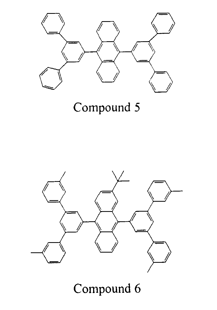
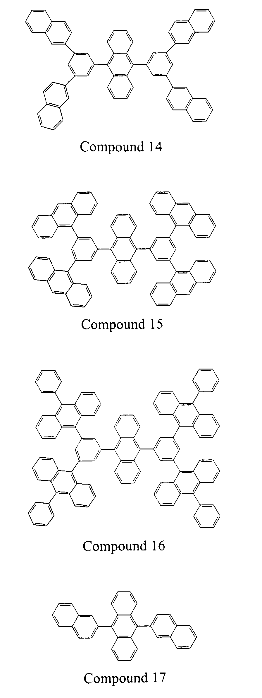
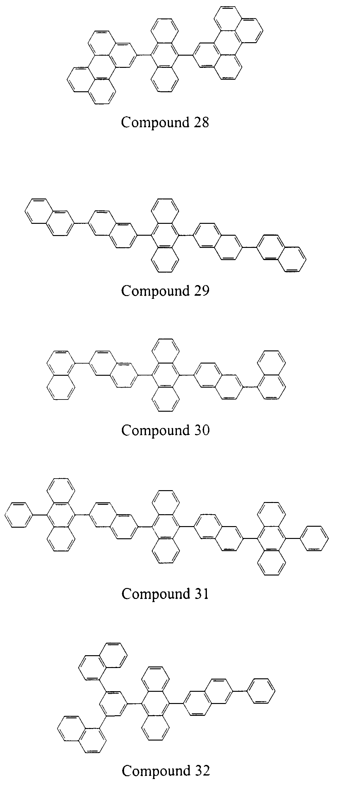
- the new hole transport materials in this invention include aromatic hydrocarbons or fused aromatic hydrocarbons with a molecular structure containing at least 20 carbon atoms and have an ionization potential greater than 5.0 eV;
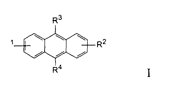
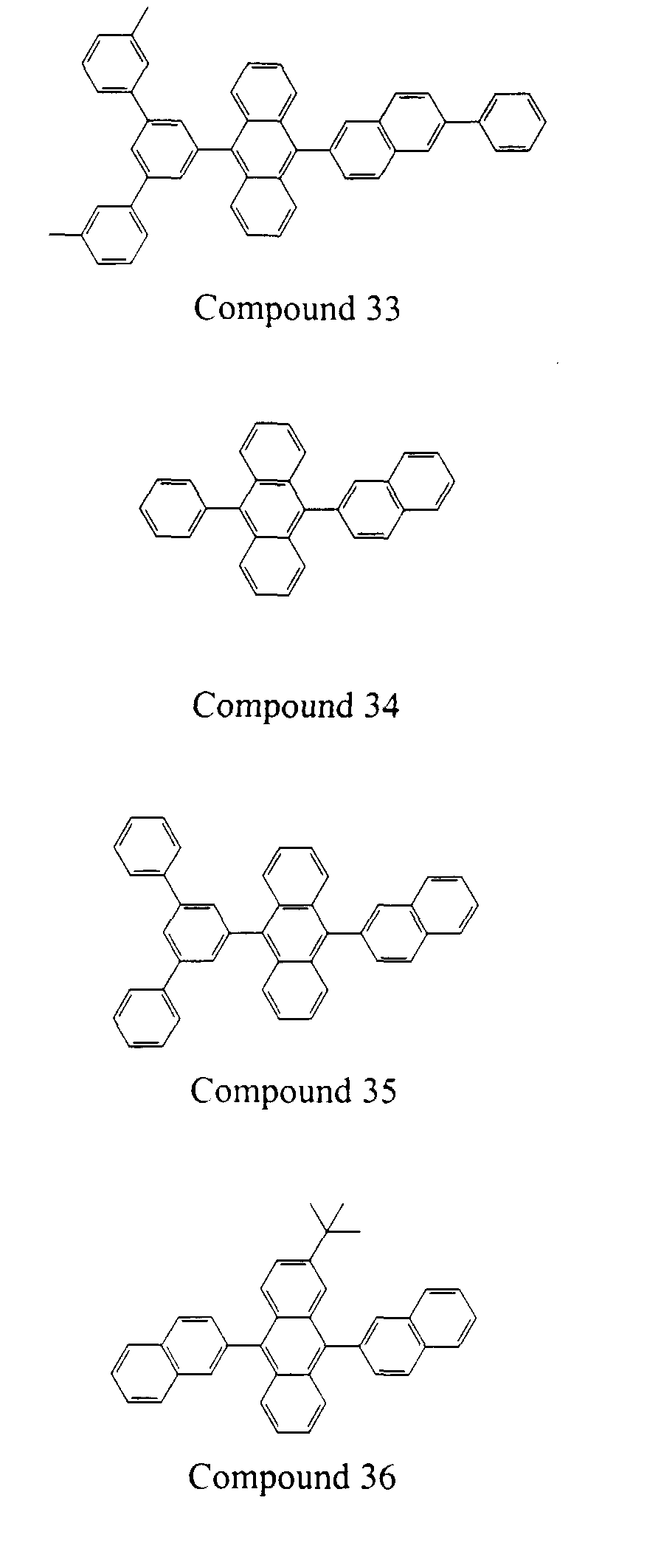
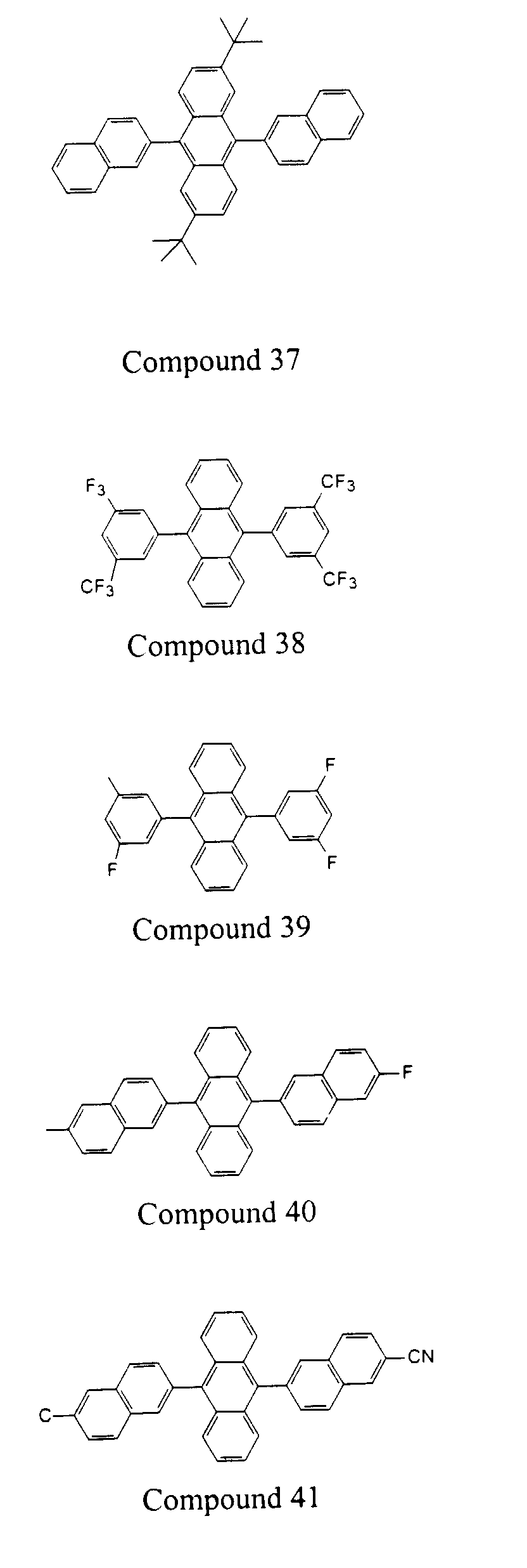
- a representative class of the hole transport materials includes anthracene derivatives of formula I: wherein:
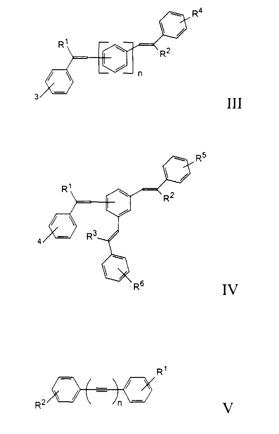
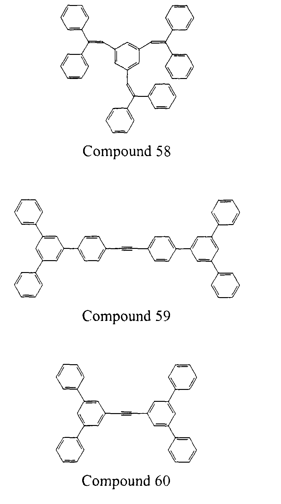
- Another representative class of the hole transport materials of this invention includes arylethylene and arylacetylene derivatives of formula II, III, IV and V. wherein:
- Another representative class of the hole transport materials of this invention includes polyphenyl hydrocarbons of formula VI: wherein:
- the ionization potentials of some of these aromatic hydrocarbon hole transport materials have been measured and their values are compared with the arylamine hole transport materials as follows. It is noted that the aromatic hydrocarbon hole transport materials generally have a higher ionization potential than the arylamines.
- a higher ionization potential for the hole transport material is more favorable for hole injection from the hole transport layer to the electron transport layer in a bi-layer EL device resulting in a lower hole injection barrier and consequently a higher EL luminous efficiency.
- a preferred range for the ionization potentials is 5.0 eV or higher.
- An alternative criteria is that it should be as high as the ionization potential of the electron transport material in the bi-layer EL device.
- a hole transport material with a high ionization potential is preferred in a bi-layer EL device because it will minimize the potential barrier for hole injection from the hole transport layer to the electron transport layer. Consequently, holes will be able to cross over the barrier requiring little or no activation energy and recombine with the electrons present in the electron transport layer to produce electroluminescence.
- a criteria for the ionization potential for the hole transport material is that it should be as high as the ionization potential of the electron transport material used in the bi-layer EL device.
- Electron-transport materials used in organic EL devices generally have ionization potentials greater than 5.0 eV.
- Alq a well-known electron-transport and emissive material
- ionization potential 5.7 eV.
- Values of ionization potentials for other known electron transport materials are as follows: 5.9 eV for PBD of diazole derivatives, C. Adachi et al., Appl. Phys. Lett. 55 (15), 9, pgs. 1489-1491, October 1989; 6.1 eV for TPBI of arylbenzimidizoles, commonly assigned US-A-5,766,799.
- a useful range for the ionization potential of the hole-transport material is 5.0 eV or greater.
- the hole transport materials of this invention can be deposited by a number of methods.
- the preferred method is by vacuum vapor deposition as these aromatic hydrocarbons have good thermal stability and can be sublimed into thin film. Alternately, they can be dissolved in appropriate solvents and be cast into layers or thin films. Other deposition methods such as printing by the inkjet method, thermal transfer, laser abrasion and sputtering are useful.
- the bi-layer EL device is the basic structure providing high luminous efficiencies and low-voltage operation.
- Alternative EL device structures have been demonstrated providing improved device performance.
- These alternative device structures include features in addition to the basic bi-layer structure such as the following structure (a) hole injection layer as disclosed in US-A-4,356,429; (b) cathode modification with alkaline or alkaline halides as disclosed in US-A-5,776,622; (c) anode modification with plasma-deposited flurocarbons, and (d) doped emitter layer inserted between the hole transport and electron transport layer as disclosed in US-A-4,769,292.
- These EL device structures retain the hole transport layer as one the component of the electroluminescent medium. Therefore, the aromatic hydrocarbon or fused hydrocarbon hole transport materials disclosed in this invention are applicable to these EL device structures as well.
- the color of the EL devices can be tuned by using fluorescent dyes of different emission wavelengths.
- fluorescent dyes of different emission wavelengths By using a mixture of fluorescent dyes, EL color characteristics of the combined spectra of the individual fluorescent dyes are produced. This dopant scheme has been described in considerable details for EL devices in commonly-assigned US-A-4,769,292.
- Preferred host materials for the emissive layer of the organic EL device disclosed in this invention are metal chelated oxinoid compounds, including chelates of oxine itself (also commonly referred to as 8-quinolinol or 8-hydroxyquinoline or Alq).
- Another class of preferred host materials is a mix ligand 8-quinolinolato aluminum chelates which have been disclosed in US-A-5,141,671.
- Another class of preferred host materials is distrylstibene derivatives as disclosed in US-A-5,366,811.
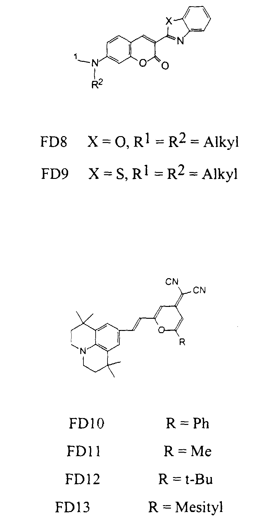
- Preferred fluorescent dyes used as the dopant in the emissive layer include coumarins, stilbenes, distrylstilbenes, derivatives of anthracene, tetracene, perylenes, rhodamines, and arylamines
- the molecular structures of the preferred fluorescent dyes for the emissive layer in the EL device are listed as follows:
- Preferred materials for use in forming the electron transporting layer of the organic EL device are metal chelated oxinoid compounds, including chelates of oxine itself (also commonly referred to as 8-quinolinol or 8-hydroxyquinoline).
- Representative compounds are 8-hydroquinoline of the group III metals such as Al, In, Mg; and of the group II metals such as Mg, Zn; and of the group I metal such as Li.
- Preferred materials for use in forming the anode of the EL device of this invention are indium tin oxide or an anode modified with fluorocarbons.
- Preferred materials for use in forming the cathode of the EL devices of this invention are Mg, Li, or alloys of these materials as disclosed in US-A-5,429,884; and commonly-assigned US-A-5,776,622 by Tang, Hung and others.
- reaction mixture was stirred under reflux for another two hours. After the reaction mixture was cooled, it was quenched by slowly adding 25.0 mL of 5% HCl with stirring. Then the solvents were removed via a rotary evaporator. The residue was dissolved in dichloromethane and washed with 0.1 M HCl followed by water. After removal of solvents, the crude residue was purified by crystallizing from heptane. A 57.0g of pure 3,5-di(1-naphthyl) bromobenzene was collected. Yield 63.5%.
- the organic EL medium has an anode, a hole transport layer, an emissive and electron transport layer, and a cathode.
- the substrate was glass.
- the above deposition sequence was completed in a single sequence without a vacuum break between the deposition of individual layers.
- the completed EL device was then sealed with a cover glass plate in a dry glove box for protection against ambient environment.
- a desiccant material was also include in the sealed package to improve the storage life of the EL device.
- Example 10 is a comparative example.
- Compound 3 used in this example is an arylamine.
- the light output and luminous efficiency obtained this EL device were substantially lower in comparison with the EL devices of Examples 11 - 18, which used aromatic hydrocarbons as the hole transport layer.
- An efficiency gain on the order of 30 to 40% has been realized by using an aromatic hydrocarbon as the hole transport layer.
- the organic EL medium has an anode, a hole transport layer, an emissive layer, an electron-transport layer, and a cathode.
- the substrate was glass.
- the above deposition sequence was completed in a single sequence without a vacuum break between the deposition of individual layers.
- the completed EL device was then sealed with a cover glass plate in a dry glove box for protection against ambient environment.
- a desiccant material was also include in the sealed package to improve the storage life of the EL device.
Landscapes
- Physics & Mathematics (AREA)
- Spectroscopy & Molecular Physics (AREA)
- Chemical & Material Sciences (AREA)
- Engineering & Computer Science (AREA)
- Materials Engineering (AREA)
- Optics & Photonics (AREA)
- Electroluminescent Light Sources (AREA)
Abstract
Description












| Hole transport layer | Electron transport and emissive layer | Applied Voltage (V) | Brightness (cd/m2) | Efficiency (cd/A) | Color | |
| Example 10 | Compound 3 | Alq | 7.5 | 578 | 2.9 | Green |
| Example 11 | Compound 61 | Alq | 16.1 | 433 | 2.17 | Green |
| Example 12 | Compound 17 | Alq | 6.3 | 855 | 4.2 | Green |
| Example 13 | Compound 11 | Alq | 8.9 | 929 | 4.65 | Green |
| Example 14 | Compound 12 | Alq | 10.7 | 877 | 4.22 | Green |
| Example 15 | Compound 36 | Alq | 8.6 | 820 | 4.10 | Green |
| Example 16 | Compound 53 | Alq | 9.0 | 726 | 3.63 | Green |
| Example 17 | Compound 54 | Alq | 7.8 | 836 | 4.18 | Green |
| Example 18 | Compound 45 | Alq | 8.5 | 879 | 4.39 | Green |
| Examples | Hole transport layer | Doped emissive layer | Electron transport layer | Applied Voltage (V) | Brightness (cd/m2) @ 20 mA/cm^2 | Efficiency cd/A | Emitting Light |
| Example 19 | Compound 3 | Alq + 1%FD 9 | Alq | 6.9 | 2219 | 11.1 | Green |
| Example 20 | Compound 17 | Alq + 1%FD 9 | Alq | 6.5 | 2994 | 14.9 | Green |
| Example 21 | Compound 12 | Alq + 1%FD 9 | Alq | 8.3 | 3133 | 15.6 | Green |
| Example 22 | Compound 45 | Alq + 1%FD 9 | Alq | 8.5 | 2848 | 14.24 | Green |
| Example 23 | Compound 46 | Alq + 1%FD 9 | Alq | 7.4 | 1242 | 6.21 | Green |
| Example 24 | Compound 3 | Alq + 1%FD 13 | Alq | 7.9 | 439 | 2.20 | Red |
| Example 25 | Compound 17 | Alq + 1%FD 13 | Alq | 7.7 | 791 | 3.90 | Red |
- 10
- substrate
- 20
- anode
- 30
- hole transport layer
- 40
- electron transport layer
- 50
- organic EL medium
- 60
- cathode
- 100
- substrate
- 200
- anode
- 300
- hole transport layer
- 400
- emissive layer
- 500
- electron transport layer
- 600
- EL medium
- 700
- cathode
Claims (4)
- An organic electroluminescent device, comprising:an anode and cathode and therebetween a hole transport layer; and an electron tranport layer disposed in an operative relationship with the hole transport layer; wherein:the hole transport layer includes at least an aromatic hydrocarbon or fused hydrocarbon containing at least 20 carbon atoms and having an ionization potential greater than 5.0 eV.
- An organic electroluminescent device, comprising:an anode and cathode and therebetween a hole transport layer; and an electron tranport layer disposed in an operative relationship with the hole transport layer the electron transport layer having at least two portions, the first portion including a fluorescent dye and the second portion providing an electron transport function, wherein;the hole transport layer includes at least an aromatic hydrocarbon or fused hydrocarbon containing at least 20 carbon atoms and having an ionization potential greater than 5.0 eV.
- The organic electroluminscent device of claim 2wherein the fluorescent dye is selected to emit light substantially in the red, green or blue portions of the spectrum.
- The organic electroluminscent device of claim 2 wherein the fluorescent dye is a mixture of dyes is selected to emit light in substantially different portions of the spectrum.
Applications Claiming Priority (2)
| Application Number | Priority Date | Filing Date | Title |
|---|---|---|---|
| US207703 | 1998-12-09 | ||
| US09/207,703 US6361886B2 (en) | 1998-12-09 | 1998-12-09 | Electroluminescent device with improved hole transport layer |
Publications (2)
| Publication Number | Publication Date |
|---|---|
| EP1009041A2 true EP1009041A2 (en) | 2000-06-14 |
| EP1009041A3 EP1009041A3 (en) | 2002-03-06 |
Family
ID=22771653
Family Applications (1)
| Application Number | Title | Priority Date | Filing Date |
|---|---|---|---|
| EP99203960A Ceased EP1009041A3 (en) | 1998-12-09 | 1999-11-25 | Electroluminescent device with improved hole transport layer |
Country Status (4)
| Country | Link |
|---|---|
| US (1) | US6361886B2 (en) |
| EP (1) | EP1009041A3 (en) |
| JP (1) | JP4772942B2 (en) |
| KR (1) | KR100793490B1 (en) |
Cited By (94)
| Publication number | Priority date | Publication date | Assignee | Title |
|---|---|---|---|---|
| WO2002038524A1 (en) * | 2000-11-08 | 2002-05-16 | Idemitsu Kosan Co., Ltd. | Organic electroluminescent element |
| WO2003043383A1 (en) * | 2001-11-12 | 2003-05-22 | Neoviewkolon Co., Ltd | Organic light-emitting device having high luminescent efficiency |
| WO2003007658A3 (en) * | 2001-07-11 | 2003-07-03 | Fuji Photo Film Co Ltd | Light-emitting device and aromatic compound |
| US6610455B1 (en) | 2002-01-30 | 2003-08-26 | Eastman Kodak Company | Making electroluminscent display devices |
| US6872472B2 (en) | 2002-02-15 | 2005-03-29 | Eastman Kodak Company | Providing an organic electroluminescent device having stacked electroluminescent units |
| US6890627B2 (en) | 2002-08-02 | 2005-05-10 | Eastman Kodak Company | Laser thermal transfer from a donor element containing a hole-transporting layer |
| US6939660B2 (en) | 2002-08-02 | 2005-09-06 | Eastman Kodak Company | Laser thermal transfer donor including a separate dopant layer |
| US7221332B2 (en) | 2003-12-19 | 2007-05-22 | Eastman Kodak Company | 3D stereo OLED display |
| US7537842B2 (en) | 2001-02-20 | 2009-05-26 | Isis Innovation Limited | Asymmetric dendrimers |
| US7592074B2 (en) | 2001-02-20 | 2009-09-22 | Isis Innovation Limited | Metal-containing dendrimers |
| US7632576B2 (en) | 2001-02-20 | 2009-12-15 | Isis Innovation Limited | Aryl-aryl dendrimers |
| EP2161272A1 (en) | 2008-09-05 | 2010-03-10 | Basf Se | Phenanthrolines |
| EP2239352A2 (en) | 2004-09-21 | 2010-10-13 | Global OLED Technology LLC | Delivering particulate material to a vaporization zone |
| EP2276089A2 (en) | 2004-07-27 | 2011-01-19 | Global OLED Technology LLC | Method for reducing moisture contamination in a top-emitting oled using a dessicant |
| WO2011015265A2 (en) | 2009-08-04 | 2011-02-10 | Merck Patent Gmbh | Electronic devices comprising multi cyclic hydrocarbons |
| WO2011032686A1 (en) | 2009-09-16 | 2011-03-24 | Merck Patent Gmbh | Formulas for producing electronic devices |
| US7947974B2 (en) | 2008-03-25 | 2011-05-24 | Global Oled Technology Llc | OLED device with hole-transport and electron-transport materials |
| WO2011076323A1 (en) | 2009-12-22 | 2011-06-30 | Merck Patent Gmbh | Formulations comprising phase-separated functional materials |
| WO2011076314A1 (en) | 2009-12-22 | 2011-06-30 | Merck Patent Gmbh | Electroluminescent formulations |
| WO2011076326A1 (en) | 2009-12-22 | 2011-06-30 | Merck Patent Gmbh | Electroluminescent functional surfactants |
| WO2011091946A1 (en) | 2010-01-30 | 2011-08-04 | Merck Patent Gmbh | Organic electroluminescent device comprising an integrated layer for colour conversion |
| EP2355198A1 (en) | 2006-05-08 | 2011-08-10 | Global OLED Technology LLC | OLED electron-injecting layer |
| US8016631B2 (en) | 2007-11-16 | 2011-09-13 | Global Oled Technology Llc | Desiccant sealing arrangement for OLED devices |
| WO2011110277A1 (en) | 2010-03-11 | 2011-09-15 | Merck Patent Gmbh | Fibers in therapy and cosmetics |
| WO2011110275A2 (en) | 2010-03-11 | 2011-09-15 | Merck Patent Gmbh | Radiative fibers |
| WO2011137922A1 (en) | 2010-05-03 | 2011-11-10 | Merck Patent Gmbh | Formulations and electronic devices |
| WO2011147522A1 (en) | 2010-05-27 | 2011-12-01 | Merck Patent Gmbh | Compositions comprising quantum dots |
| US8088500B2 (en) | 2008-11-12 | 2012-01-03 | Global Oled Technology Llc | OLED device with fluoranthene electron injection materials |
| WO2012013272A1 (en) | 2010-07-26 | 2012-02-02 | Merck Patent Gmbh | Quantum dots and hosts |
| WO2012013270A1 (en) | 2010-07-26 | 2012-02-02 | Merck Patent Gmbh | Nanocrystals in devices |
| US8129039B2 (en) | 2007-10-26 | 2012-03-06 | Global Oled Technology, Llc | Phosphorescent OLED device with certain fluoranthene host |
| DE102010055901A1 (en) | 2010-12-23 | 2012-06-28 | Merck Patent Gmbh | Organic electroluminescent device |
| US8216697B2 (en) | 2009-02-13 | 2012-07-10 | Global Oled Technology Llc | OLED with fluoranthene-macrocyclic materials |
| US8247088B2 (en) | 2008-08-28 | 2012-08-21 | Global Oled Technology Llc | Emitting complex for electroluminescent devices |
| WO2012110178A1 (en) | 2011-02-14 | 2012-08-23 | Merck Patent Gmbh | Device and method for treatment of cells and cell tissue |
| US8252434B2 (en) | 2005-06-22 | 2012-08-28 | Semiconductor Energy Laboratory Co., Ltd. | Light emitting device and electronic appliance using the same |
| EP2498317A2 (en) | 2007-07-25 | 2012-09-12 | Global OLED Technology LLC | Preventing stress transfer in OLED display components |
| US8324800B2 (en) | 2008-06-12 | 2012-12-04 | Global Oled Technology Llc | Phosphorescent OLED device with mixed hosts |
| WO2012163464A1 (en) | 2011-06-01 | 2012-12-06 | Merck Patent Gmbh | Hybrid ambipolar tfts |
| WO2013013754A1 (en) | 2011-07-25 | 2013-01-31 | Merck Patent Gmbh | Copolymers with functionalized side chains |
| EP2568515A1 (en) | 2007-10-26 | 2013-03-13 | Global OLED Technology LLC | OLED device with fluoranthene electron transport materials |
| US8420229B2 (en) | 2007-10-26 | 2013-04-16 | Global OLED Technologies LLC | OLED device with certain fluoranthene light-emitting dopants |
| US8431242B2 (en) | 2007-10-26 | 2013-04-30 | Global Oled Technology, Llc. | OLED device with certain fluoranthene host |
| WO2013060411A1 (en) | 2011-10-28 | 2013-05-02 | Merck Patent Gmbh | Hyperbranched polymers, methods for producing same, and use of same in electronic devices |
| US8628862B2 (en) | 2007-09-20 | 2014-01-14 | Basf Se | Electroluminescent device |
| EP2752866A1 (en) | 2002-08-20 | 2014-07-09 | Global OLED Technology LLC | Color organic light emitting diode display with improved lifetime |
| US8795855B2 (en) | 2007-01-30 | 2014-08-05 | Global Oled Technology Llc | OLEDs having high efficiency and excellent lifetime |
| WO2015014427A1 (en) | 2013-07-29 | 2015-02-05 | Merck Patent Gmbh | Electro-optical device and the use thereof |
| WO2015014429A1 (en) | 2013-07-29 | 2015-02-05 | Merck Patent Gmbh | Electroluminescence device |
| US9040170B2 (en) | 2004-09-20 | 2015-05-26 | Global Oled Technology Llc | Electroluminescent device with quinazoline complex emitter |
| WO2016034262A1 (en) | 2014-09-05 | 2016-03-10 | Merck Patent Gmbh | Formulations and electronic devices |
| WO2016107663A1 (en) | 2014-12-30 | 2016-07-07 | Merck Patent Gmbh | Formulations and electronic devices |
| WO2016155866A1 (en) | 2015-03-30 | 2016-10-06 | Merck Patent Gmbh | Formulation of an organic functional material comprising a siloxane solvent |
| EP3101647A1 (en) | 2002-12-16 | 2016-12-07 | Global OLED Technology LLC | A color oled display with improved power efficiency |
| WO2016198141A1 (en) | 2015-06-12 | 2016-12-15 | Merck Patent Gmbh | Esters containing non-aromatic cycles as solvents for oled formulations |
| WO2017036572A1 (en) | 2015-08-28 | 2017-03-09 | Merck Patent Gmbh | Formulation of an organic functional material comprising an epoxy group containing solvent |
| US9666826B2 (en) | 2005-11-30 | 2017-05-30 | Global Oled Technology Llc | Electroluminescent device including an anthracene derivative |
| WO2017097391A1 (en) | 2015-12-10 | 2017-06-15 | Merck Patent Gmbh | Formulations containing ketones comprising non-aromatic cycles |
| WO2017102048A1 (en) | 2015-12-15 | 2017-06-22 | Merck Patent Gmbh | Esters containing aromatic groups as solvents for organic electronic formulations |
| WO2017102049A1 (en) | 2015-12-16 | 2017-06-22 | Merck Patent Gmbh | Formulations containing a mixture of at least two different solvents |
| WO2017102052A1 (en) | 2015-12-16 | 2017-06-22 | Merck Patent Gmbh | Formulations containing a solid solvent |
| WO2017140404A1 (en) | 2016-02-17 | 2017-08-24 | Merck Patent Gmbh | Formulation of an organic functional material |
| WO2017157783A1 (en) | 2016-03-15 | 2017-09-21 | Merck Patent Gmbh | Receptacle comprising a formulation containing at least one organic semiconductor |
| WO2017216129A1 (en) | 2016-06-16 | 2017-12-21 | Merck Patent Gmbh | Formulation of an organic functional material |
| WO2017216128A1 (en) | 2016-06-17 | 2017-12-21 | Merck Patent Gmbh | Formulation of an organic functional material |
| WO2018001928A1 (en) | 2016-06-28 | 2018-01-04 | Merck Patent Gmbh | Formulation of an organic functional material |
| WO2018024719A1 (en) | 2016-08-04 | 2018-02-08 | Merck Patent Gmbh | Formulation of an organic functional material |
| WO2018077662A1 (en) | 2016-10-31 | 2018-05-03 | Merck Patent Gmbh | Formulation of an organic functional material |
| WO2018077660A1 (en) | 2016-10-31 | 2018-05-03 | Merck Patent Gmbh | Formulation of an organic functional material |
| WO2018104202A1 (en) | 2016-12-06 | 2018-06-14 | Merck Patent Gmbh | Preparation process for an electronic device |
| WO2018108760A1 (en) | 2016-12-13 | 2018-06-21 | Merck Patent Gmbh | Formulation of an organic functional material |
| WO2018114883A1 (en) | 2016-12-22 | 2018-06-28 | Merck Patent Gmbh | Mixtures comprising at least two organofunctional compounds |
| WO2018138319A1 (en) | 2017-01-30 | 2018-08-02 | Merck Patent Gmbh | Method for forming an organic electroluminescence (el) element |
| WO2018138318A1 (en) | 2017-01-30 | 2018-08-02 | Merck Patent Gmbh | Method for forming an organic element of an electronic device |
| WO2018178136A1 (en) | 2017-03-31 | 2018-10-04 | Merck Patent Gmbh | Printing method for an organic light emitting diode (oled) |
| WO2018189050A1 (en) | 2017-04-10 | 2018-10-18 | Merck Patent Gmbh | Formulation of an organic functional material |
| WO2018202603A1 (en) | 2017-05-03 | 2018-11-08 | Merck Patent Gmbh | Formulation of an organic functional material |
| WO2019016184A1 (en) | 2017-07-18 | 2019-01-24 | Merck Patent Gmbh | Formulation of an organic functional material |
| WO2019115573A1 (en) | 2017-12-15 | 2019-06-20 | Merck Patent Gmbh | Formulation of an organic functional material |
| WO2019162483A1 (en) | 2018-02-26 | 2019-08-29 | Merck Patent Gmbh | Formulation of an organic functional material |
| WO2019238782A1 (en) | 2018-06-15 | 2019-12-19 | Merck Patent Gmbh | Formulation of an organic functional material |
| US10593886B2 (en) | 2013-08-25 | 2020-03-17 | Molecular Glasses, Inc. | OLED devices with improved lifetime using non-crystallizable molecular glass mixture hosts |
| WO2020064582A1 (en) | 2018-09-24 | 2020-04-02 | Merck Patent Gmbh | Method for the production of a granular material |
| WO2020094538A1 (en) | 2018-11-06 | 2020-05-14 | Merck Patent Gmbh | Method for forming an organic element of an electronic device |
| WO2021213917A1 (en) | 2020-04-21 | 2021-10-28 | Merck Patent Gmbh | Emulsions comprising organic functional materials |
| WO2021259824A1 (en) | 2020-06-23 | 2021-12-30 | Merck Patent Gmbh | Method for producing a mixture |
| WO2022122607A1 (en) | 2020-12-08 | 2022-06-16 | Merck Patent Gmbh | An ink system and a method for inkjet printing |
| WO2022243403A1 (en) | 2021-05-21 | 2022-11-24 | Merck Patent Gmbh | Method for the continuous purification of at least one functional material and device for the continuous purification of at least one functional material |
| WO2023012084A1 (en) | 2021-08-02 | 2023-02-09 | Merck Patent Gmbh | A printing method by combining inks |
| WO2023031073A1 (en) | 2021-08-31 | 2023-03-09 | Merck Patent Gmbh | Composition |
| WO2023057327A1 (en) | 2021-10-05 | 2023-04-13 | Merck Patent Gmbh | Method for forming an organic element of an electronic device |
| WO2023237458A1 (en) | 2022-06-07 | 2023-12-14 | Merck Patent Gmbh | Method of printing a functional layer of an electronic device by combining inks |
| WO2024126635A1 (en) | 2022-12-16 | 2024-06-20 | Merck Patent Gmbh | Formulation of an organic functional material |
| WO2025032039A1 (en) | 2023-08-07 | 2025-02-13 | Merck Patent Gmbh | Process for the preparation of an electronic device |
Families Citing this family (77)
| Publication number | Priority date | Publication date | Assignee | Title |
|---|---|---|---|---|
| EP1009043A3 (en) * | 1998-12-09 | 2002-07-03 | Eastman Kodak Company | Electroluminescent device with polyphenyl hydrocarbon hole transport layer |
| DE69841627D1 (en) * | 1998-12-15 | 2010-06-02 | Max Planck Inst Fuer Polymerfo | Functional material-containing polyimide layer, device using it, and method of making this device |
| TWI282697B (en) * | 2000-02-25 | 2007-06-11 | Seiko Epson Corp | Organic electroluminescence device |
| US6936485B2 (en) * | 2000-03-27 | 2005-08-30 | Semiconductor Energy Laboratory Co., Ltd. | Method of manufacturing a light emitting device |
| JP4094203B2 (en) * | 2000-03-30 | 2008-06-04 | 出光興産株式会社 | Organic electroluminescence device and organic light emitting medium |
| JP4026336B2 (en) * | 2000-08-11 | 2007-12-26 | セイコーエプソン株式会社 | Manufacturing method of organic EL device |
| US6746784B2 (en) * | 2000-11-07 | 2004-06-08 | Samsung Electronics Co., Ltd. | Organic electroluminescent device |
| US6720090B2 (en) * | 2001-01-02 | 2004-04-13 | Eastman Kodak Company | Organic light emitting diode devices with improved luminance efficiency |
| KR100916231B1 (en) * | 2001-03-14 | 2009-09-08 | 더 트러스티즈 오브 프린스턴 유니버시티 | Materials and apparatus for blue phosphorescent organic light emitting diodes |
| US6565996B2 (en) * | 2001-06-06 | 2003-05-20 | Eastman Kodak Company | Organic light-emitting device having a color-neutral dopant in a hole-transport layer and/or in an electron-transport layer |
| JP4700029B2 (en) * | 2001-07-11 | 2011-06-15 | 富士フイルム株式会社 | Light emitting element |
| US6727644B2 (en) * | 2001-08-06 | 2004-04-27 | Eastman Kodak Company | Organic light-emitting device having a color-neutral dopant in an emission layer and in a hole and/or electron transport sublayer |
| KR100528322B1 (en) * | 2001-09-28 | 2005-11-15 | 삼성에스디아이 주식회사 | Blue Electroluminescent Polymer And Organo-electroluminescent Device Using Thereof |
| AU2002323418A1 (en) | 2002-04-08 | 2003-10-27 | The University Of Southern California | Doped organic carrier transport materials |
| AU2003230308A1 (en) * | 2002-05-07 | 2003-11-11 | Lg Chem, Ltd. | New organic compounds for electroluminescence and organic electroluminescent devices using the same |
| KR20040005416A (en) * | 2002-07-10 | 2004-01-16 | 엘지전자 주식회사 | Compound For Blue Light Emitting Material And Organic Electroluminescent Device Comprising The Same |
| US7169482B2 (en) * | 2002-07-26 | 2007-01-30 | Lg.Philips Lcd Co., Ltd. | Display device with anthracene and triazine derivatives |
| US20040031965A1 (en) * | 2002-08-16 | 2004-02-19 | Forrest Stephen R. | Organic photonic integrated circuit using an organic photodetector and a transparent organic light emitting device |
| US20040043138A1 (en) * | 2002-08-21 | 2004-03-04 | Ramesh Jagannathan | Solid state lighting using compressed fluid coatings |
| US7839074B2 (en) * | 2002-08-23 | 2010-11-23 | Idemitsu Kosan Co., Ltd. | Organic electroluminescence device and anthracene derivative |
| US20040048099A1 (en) * | 2002-08-29 | 2004-03-11 | Chen Jian Ping | Organic light-emitting device using iptycene derivatives |
| US7053412B2 (en) * | 2003-06-27 | 2006-05-30 | The Trustees Of Princeton University And Universal Display Corporation | Grey scale bistable display |
| US6852429B1 (en) | 2003-08-06 | 2005-02-08 | Canon Kabushiki Kaisha | Organic electroluminescent device based on pyrene derivatives |
| US7887931B2 (en) * | 2003-10-24 | 2011-02-15 | Global Oled Technology Llc | Electroluminescent device with anthracene derivative host |
| US7056601B2 (en) * | 2003-10-24 | 2006-06-06 | Eastman Kodak Company | OLED device with asymmetric host |
| WO2011143510A1 (en) | 2010-05-12 | 2011-11-17 | Lynk Labs, Inc. | Led lighting system |
| US10575376B2 (en) | 2004-02-25 | 2020-02-25 | Lynk Labs, Inc. | AC light emitting diode and AC LED drive methods and apparatus |
| US10499465B2 (en) | 2004-02-25 | 2019-12-03 | Lynk Labs, Inc. | High frequency multi-voltage and multi-brightness LED lighting devices and systems and methods of using same |
| JP4789475B2 (en) | 2004-03-10 | 2011-10-12 | 富士フイルム株式会社 | Light emitting element |
| US7326371B2 (en) * | 2004-03-25 | 2008-02-05 | Eastman Kodak Company | Electroluminescent device with anthracene derivative host |
| US7550915B2 (en) * | 2004-05-11 | 2009-06-23 | Osram Opto Semiconductors Gmbh | Organic electronic device with hole injection |
| US20060003487A1 (en) * | 2004-06-30 | 2006-01-05 | Intel Corporation | Low power consumption OLED material for display applications |
| JP2006054422A (en) * | 2004-07-15 | 2006-02-23 | Fuji Photo Film Co Ltd | Organic electroluminescent device and display device |
| KR100669717B1 (en) * | 2004-07-29 | 2007-01-16 | 삼성에스디아이 주식회사 | Organic electroluminescent element |
| KR100669757B1 (en) * | 2004-11-12 | 2007-01-16 | 삼성에스디아이 주식회사 | Organic electroluminescent element |
| US7351999B2 (en) * | 2004-12-16 | 2008-04-01 | Au Optronics Corporation | Organic light-emitting device with improved layer structure |
| US8950328B1 (en) | 2004-12-29 | 2015-02-10 | E I Du Pont De Nemours And Company | Methods of fabricating organic electronic devices |
| WO2006104044A1 (en) * | 2005-03-28 | 2006-10-05 | Idemitsu Kosan Co., Ltd. | Anthrylarylene derivative, material for organic electroluminescent device, and organic electroluminescent device using same |
| JP2006290771A (en) * | 2005-04-08 | 2006-10-26 | Akita Univ | Anthracene-based organic zeolite analogues, production methods and uses thereof |
| US8057916B2 (en) | 2005-04-20 | 2011-11-15 | Global Oled Technology, Llc. | OLED device with improved performance |
| CN101203968B (en) * | 2005-04-21 | 2010-05-19 | 株式会社半导体能源研究所 | Light-emitting element, light-emitting device, and electronic apparatus |
| EP1724852A3 (en) * | 2005-05-20 | 2010-01-27 | Semiconductor Energy Laboratory Co., Ltd. | Light emitting element, light emitting device, and electronic device |
| WO2006130598A2 (en) | 2005-05-31 | 2006-12-07 | Universal Display Corporation | Triphenylene hosts in phosphorescent light emitting diodes |
| JP5072271B2 (en) * | 2005-06-22 | 2012-11-14 | 株式会社半導体エネルギー研究所 | LIGHT EMITTING DEVICE AND ELECTRONIC DEVICE USING THE SAME |
| US8766023B2 (en) | 2005-07-20 | 2014-07-01 | Lg Display Co., Ltd. | Synthesis process |
| EP1911079A4 (en) | 2005-07-25 | 2012-05-09 | Semiconductor Energy Lab | Light-emitting element, light-emitting device, and electronic appliance |
| WO2007026587A1 (en) * | 2005-08-29 | 2007-03-08 | Semiconductor Energy Laboratory Co., Ltd. | Anthracene derivative and hole transporting material, light emitting element, and electronic appliance using the same |
| US9112170B2 (en) * | 2006-03-21 | 2015-08-18 | Semiconductor Energy Laboratory Co., Ltd. | Light-emitting element, light-emitting device, and electronic device |
| US8945722B2 (en) * | 2006-10-27 | 2015-02-03 | The University Of Southern California | Materials and architectures for efficient harvesting of singlet and triplet excitons for white light emitting OLEDs |
| US11317495B2 (en) | 2007-10-06 | 2022-04-26 | Lynk Labs, Inc. | LED circuits and assemblies |
| US11297705B2 (en) | 2007-10-06 | 2022-04-05 | Lynk Labs, Inc. | Multi-voltage and multi-brightness LED lighting devices and methods of using same |
| JP4628435B2 (en) * | 2008-02-14 | 2011-02-09 | 財団法人山形県産業技術振興機構 | Organic electroluminescence device |
| ATE540069T1 (en) * | 2008-02-29 | 2012-01-15 | Plextronics Inc | PLANNING EQUIPMENT AND DEVICES |
| US7931975B2 (en) | 2008-11-07 | 2011-04-26 | Global Oled Technology Llc | Electroluminescent device containing a flouranthene compound |
| US7968215B2 (en) | 2008-12-09 | 2011-06-28 | Global Oled Technology Llc | OLED device with cyclobutene electron injection materials |
| US20130306961A1 (en) * | 2011-02-11 | 2013-11-21 | Idemitsu Kosen Co. Ltd | Organic light emitting device and materials for use in same |
| WO2012122387A1 (en) * | 2011-03-10 | 2012-09-13 | Marshall Cox | Graphene electrodes for electronic devices |
| EP2503618B1 (en) | 2011-03-23 | 2014-01-01 | Semiconductor Energy Laboratory Co., Ltd. | Composite material, light-emitting element, light-emitting device, electronic device, and lighting device |
| TWI602334B (en) | 2011-05-13 | 2017-10-11 | 半導體能源研究所股份有限公司 | Light-emitting element and light-emitting device |
| US9419239B2 (en) * | 2011-07-08 | 2016-08-16 | Semiconductor Energy Laboratory Co., Ltd. | Composite material, light-emitting element, light-emitting device, electronic device, lighting device, and organic compound |
| US20140239809A1 (en) | 2011-08-18 | 2014-08-28 | Lynk Labs, Inc. | Devices and systems having ac led circuits and methods of driving the same |
| US9247597B2 (en) | 2011-12-02 | 2016-01-26 | Lynk Labs, Inc. | Color temperature controlled and low THD LED lighting devices and systems and methods of driving the same |
| US8546617B1 (en) | 2012-03-23 | 2013-10-01 | Empire Technology Development Llc | Dioxaborinanes and uses thereof |
| US9290598B2 (en) | 2012-03-29 | 2016-03-22 | Empire Technology Development Llc | Dioxaborinane co-polymers and uses thereof |
| US9095141B2 (en) | 2012-07-31 | 2015-08-04 | Empire Technology Development Llc | Antifouling compositions including dioxaborinanes and uses thereof |
| KR101468089B1 (en) * | 2013-04-08 | 2014-12-05 | 주식회사 엘엠에스 | Novel compound, light-emitting device including the compound and electronic device |
| JP6210745B2 (en) * | 2013-06-11 | 2017-10-11 | キヤノン株式会社 | Organic light emitting device |
| KR102086555B1 (en) * | 2013-08-14 | 2020-03-10 | 삼성디스플레이 주식회사 | Anthracene-based compounds and Organic light emitting device comprising the same |
| CN108117770A (en) * | 2016-11-30 | 2018-06-05 | 苏州百源基因技术有限公司 | A kind of blue light excitation fluorescent dye and preparation method and application |
| CN116583131A (en) | 2017-04-26 | 2023-08-11 | Oti照明公司 | Method for patterning a coating on a surface and apparatus comprising the patterned coating |
| US11079077B2 (en) | 2017-08-31 | 2021-08-03 | Lynk Labs, Inc. | LED lighting system and installation methods |
| US11751415B2 (en) | 2018-02-02 | 2023-09-05 | Oti Lumionics Inc. | Materials for forming a nucleation-inhibiting coating and devices incorporating same |
| JP7390739B2 (en) | 2019-03-07 | 2023-12-04 | オーティーアイ ルミオニクス インコーポレーテッド | Materials for forming nucleation-inhibiting coatings and devices incorporating the same |
| KR102831863B1 (en) | 2019-04-18 | 2025-07-10 | 오티아이 루미오닉스 인크. | Material for forming a nucleation-inhibiting coating and device comprising the same |
| JP7576337B2 (en) | 2019-05-08 | 2024-11-01 | オーティーアイ ルミオニクス インコーポレーテッド | Materials for forming nucleation-inhibiting coatings and devices incorporating same - Patents.com |
| CN114843413B (en) * | 2020-06-11 | 2025-12-02 | 云谷(固安)科技有限公司 | Light-emitting devices and display panels |
| WO2022123431A1 (en) | 2020-12-07 | 2022-06-16 | Oti Lumionics Inc. | Patterning a conductive deposited layer using a nucleation inhibiting coating and an underlying metallic coating |
Family Cites Families (20)
| Publication number | Priority date | Publication date | Assignee | Title |
|---|---|---|---|---|
| US3172862A (en) | 1960-09-29 | 1965-03-09 | Dow Chemical Co | Organic electroluminescent phosphors |
| US3173050A (en) | 1962-09-19 | 1965-03-09 | Dow Chemical Co | Electroluminescent cell |
| US3710167A (en) | 1970-07-02 | 1973-01-09 | Rca Corp | Organic electroluminescent cells having a tunnel injection cathode |
| US4356429A (en) | 1980-07-17 | 1982-10-26 | Eastman Kodak Company | Organic electroluminescent cell |
| US4539507A (en) | 1983-03-25 | 1985-09-03 | Eastman Kodak Company | Organic electroluminescent devices having improved power conversion efficiencies |
| US4769292A (en) | 1987-03-02 | 1988-09-06 | Eastman Kodak Company | Electroluminescent device with modified thin film luminescent zone |
| US5061569A (en) | 1990-07-26 | 1991-10-29 | Eastman Kodak Company | Electroluminescent device with organic electroluminescent medium |
| WO1992005131A1 (en) | 1990-09-20 | 1992-04-02 | Idemitsu Kosan Co., Ltd. | Organic electroluminescent element |
| US5141671A (en) | 1991-08-01 | 1992-08-25 | Eastman Kodak Company | Mixed ligand 8-quinolinolato aluminum chelate luminophors |
| JP3179234B2 (en) * | 1992-03-27 | 2001-06-25 | パイオニア株式会社 | Organic electroluminescence device |
| US5652067A (en) * | 1992-09-10 | 1997-07-29 | Toppan Printing Co., Ltd. | Organic electroluminescent device |
| JP3534445B2 (en) * | 1993-09-09 | 2004-06-07 | 隆一 山本 | EL device using polythiophene |
| JP3642606B2 (en) * | 1994-04-28 | 2005-04-27 | Tdk株式会社 | Organic EL device |
| US5554450A (en) | 1995-03-08 | 1996-09-10 | Eastman Kodak Company | Organic electroluminescent devices with high thermal stability |
| WO1997044829A1 (en) * | 1996-05-22 | 1997-11-27 | Organet Chemical Co., Ltd. | Molecule dispersion type negative resistance element and method for manufacturing the same |
| US5776622A (en) | 1996-07-29 | 1998-07-07 | Eastman Kodak Company | Bilayer eletron-injeting electrode for use in an electroluminescent device |
| US5766779A (en) | 1996-08-20 | 1998-06-16 | Eastman Kodak Company | Electron transporting materials for organic electroluminescent devices |
| US5885498A (en) * | 1996-12-11 | 1999-03-23 | Matsushita Electric Industrial Co., Ltd. | Organic light emitting device and method for producing the same |
| US5989737A (en) * | 1997-02-27 | 1999-11-23 | Xerox Corporation | Organic electroluminescent devices |
| US5972247A (en) * | 1998-03-20 | 1999-10-26 | Eastman Kodak Company | Organic electroluminescent elements for stable blue electroluminescent devices |
-
1998
- 1998-12-09 US US09/207,703 patent/US6361886B2/en not_active Expired - Lifetime
-
1999
- 1999-11-25 EP EP99203960A patent/EP1009041A3/en not_active Ceased
- 1999-12-08 KR KR1019990055946A patent/KR100793490B1/en not_active Expired - Lifetime
- 1999-12-08 JP JP34839699A patent/JP4772942B2/en not_active Expired - Lifetime
Cited By (117)
| Publication number | Priority date | Publication date | Assignee | Title |
|---|---|---|---|---|
| CN100445245C (en) * | 2000-11-08 | 2008-12-24 | 出光兴产株式会社 | organic electroluminescent element |
| US7361796B2 (en) | 2000-11-08 | 2008-04-22 | Idemitsu Kosan Co., Ltd. | Orangic electroluminescence device |
| US7053255B2 (en) | 2000-11-08 | 2006-05-30 | Idemitsu Kosan Co., Ltd. | Substituted diphenylanthracene compounds for organic electroluminescence devices |
| WO2002038524A1 (en) * | 2000-11-08 | 2002-05-16 | Idemitsu Kosan Co., Ltd. | Organic electroluminescent element |
| US8319213B2 (en) | 2001-02-20 | 2012-11-27 | Isis Innovation Limited | Aryl-aryl dendrimers |
| US7960725B2 (en) | 2001-02-20 | 2011-06-14 | Isis Innovation Limited | Aryl-aryl dendrimers |
| US8314549B2 (en) | 2001-02-20 | 2012-11-20 | Isis Innovation Limited | Metal-containing dendrimers |
| US7906902B2 (en) | 2001-02-20 | 2011-03-15 | Isis Innovation Limited | Metal-containing dendrimers |
| US7960557B2 (en) | 2001-02-20 | 2011-06-14 | Isis Innovation Limited | Asymmetric dendrimers |
| US7632576B2 (en) | 2001-02-20 | 2009-12-15 | Isis Innovation Limited | Aryl-aryl dendrimers |
| US7537842B2 (en) | 2001-02-20 | 2009-05-26 | Isis Innovation Limited | Asymmetric dendrimers |
| US7592074B2 (en) | 2001-02-20 | 2009-09-22 | Isis Innovation Limited | Metal-containing dendrimers |
| CN1302087C (en) * | 2001-07-11 | 2007-02-28 | 富士胶片株式会社 | Light-emitting device and aromatic compound |
| WO2003007658A3 (en) * | 2001-07-11 | 2003-07-03 | Fuji Photo Film Co Ltd | Light-emitting device and aromatic compound |
| US7733012B2 (en) | 2001-07-11 | 2010-06-08 | Fujifilm Corporation | Light-emitting device and aromatic compound |
| US7517592B2 (en) * | 2001-07-11 | 2009-04-14 | Fujifilm Corporation | Light-emitting device and aromatic compound |
| EP1444869A4 (en) * | 2001-11-12 | 2008-05-28 | Neoviewkolon Co Ltd | HIGHLY EFFICIENT LUMINESCENCE ORGANIC ELECTROLUMINESCENCE DEVICE |
| WO2003043383A1 (en) * | 2001-11-12 | 2003-05-22 | Neoviewkolon Co., Ltd | Organic light-emitting device having high luminescent efficiency |
| US6610455B1 (en) | 2002-01-30 | 2003-08-26 | Eastman Kodak Company | Making electroluminscent display devices |
| US6872472B2 (en) | 2002-02-15 | 2005-03-29 | Eastman Kodak Company | Providing an organic electroluminescent device having stacked electroluminescent units |
| US6939660B2 (en) | 2002-08-02 | 2005-09-06 | Eastman Kodak Company | Laser thermal transfer donor including a separate dopant layer |
| US6890627B2 (en) | 2002-08-02 | 2005-05-10 | Eastman Kodak Company | Laser thermal transfer from a donor element containing a hole-transporting layer |
| EP2752866A1 (en) | 2002-08-20 | 2014-07-09 | Global OLED Technology LLC | Color organic light emitting diode display with improved lifetime |
| EP3101691A1 (en) | 2002-12-16 | 2016-12-07 | Global OLED Technology LLC | A color oled display with improved power efficiency |
| EP3101647A1 (en) | 2002-12-16 | 2016-12-07 | Global OLED Technology LLC | A color oled display with improved power efficiency |
| US7221332B2 (en) | 2003-12-19 | 2007-05-22 | Eastman Kodak Company | 3D stereo OLED display |
| EP2276089A2 (en) | 2004-07-27 | 2011-01-19 | Global OLED Technology LLC | Method for reducing moisture contamination in a top-emitting oled using a dessicant |
| US9040170B2 (en) | 2004-09-20 | 2015-05-26 | Global Oled Technology Llc | Electroluminescent device with quinazoline complex emitter |
| EP2239352A2 (en) | 2004-09-21 | 2010-10-13 | Global OLED Technology LLC | Delivering particulate material to a vaporization zone |
| US8815419B2 (en) | 2005-06-22 | 2014-08-26 | Semiconductor Energy Laboratory Co., Ltd. | Light emitting device and electronic appliance using the same |
| US8541114B2 (en) | 2005-06-22 | 2013-09-24 | Semiconductor Energy Laboratory Co., Ltd. | Light emitting device and electronic appliance using the same |
| US8252434B2 (en) | 2005-06-22 | 2012-08-28 | Semiconductor Energy Laboratory Co., Ltd. | Light emitting device and electronic appliance using the same |
| US9666826B2 (en) | 2005-11-30 | 2017-05-30 | Global Oled Technology Llc | Electroluminescent device including an anthracene derivative |
| EP2355198A1 (en) | 2006-05-08 | 2011-08-10 | Global OLED Technology LLC | OLED electron-injecting layer |
| US9620721B2 (en) | 2007-01-30 | 2017-04-11 | Global Oled Technology Llc | OLEDs having high efficiency and excellent lifetime |
| US8795855B2 (en) | 2007-01-30 | 2014-08-05 | Global Oled Technology Llc | OLEDs having high efficiency and excellent lifetime |
| EP2498317A2 (en) | 2007-07-25 | 2012-09-12 | Global OLED Technology LLC | Preventing stress transfer in OLED display components |
| US8628862B2 (en) | 2007-09-20 | 2014-01-14 | Basf Se | Electroluminescent device |
| US8431242B2 (en) | 2007-10-26 | 2013-04-30 | Global Oled Technology, Llc. | OLED device with certain fluoranthene host |
| US8420229B2 (en) | 2007-10-26 | 2013-04-16 | Global OLED Technologies LLC | OLED device with certain fluoranthene light-emitting dopants |
| EP2568515A1 (en) | 2007-10-26 | 2013-03-13 | Global OLED Technology LLC | OLED device with fluoranthene electron transport materials |
| US8129039B2 (en) | 2007-10-26 | 2012-03-06 | Global Oled Technology, Llc | Phosphorescent OLED device with certain fluoranthene host |
| US8016631B2 (en) | 2007-11-16 | 2011-09-13 | Global Oled Technology Llc | Desiccant sealing arrangement for OLED devices |
| US7947974B2 (en) | 2008-03-25 | 2011-05-24 | Global Oled Technology Llc | OLED device with hole-transport and electron-transport materials |
| US8324800B2 (en) | 2008-06-12 | 2012-12-04 | Global Oled Technology Llc | Phosphorescent OLED device with mixed hosts |
| US8247088B2 (en) | 2008-08-28 | 2012-08-21 | Global Oled Technology Llc | Emitting complex for electroluminescent devices |
| EP2161272A1 (en) | 2008-09-05 | 2010-03-10 | Basf Se | Phenanthrolines |
| US8088500B2 (en) | 2008-11-12 | 2012-01-03 | Global Oled Technology Llc | OLED device with fluoranthene electron injection materials |
| US8216697B2 (en) | 2009-02-13 | 2012-07-10 | Global Oled Technology Llc | OLED with fluoranthene-macrocyclic materials |
| WO2011015265A2 (en) | 2009-08-04 | 2011-02-10 | Merck Patent Gmbh | Electronic devices comprising multi cyclic hydrocarbons |
| WO2011032686A1 (en) | 2009-09-16 | 2011-03-24 | Merck Patent Gmbh | Formulas for producing electronic devices |
| WO2011076323A1 (en) | 2009-12-22 | 2011-06-30 | Merck Patent Gmbh | Formulations comprising phase-separated functional materials |
| WO2011076314A1 (en) | 2009-12-22 | 2011-06-30 | Merck Patent Gmbh | Electroluminescent formulations |
| WO2011076326A1 (en) | 2009-12-22 | 2011-06-30 | Merck Patent Gmbh | Electroluminescent functional surfactants |
| WO2011091946A1 (en) | 2010-01-30 | 2011-08-04 | Merck Patent Gmbh | Organic electroluminescent device comprising an integrated layer for colour conversion |
| DE102010006280A1 (en) | 2010-01-30 | 2011-08-04 | Merck Patent GmbH, 64293 | color conversion |
| WO2011110277A1 (en) | 2010-03-11 | 2011-09-15 | Merck Patent Gmbh | Fibers in therapy and cosmetics |
| WO2011110275A2 (en) | 2010-03-11 | 2011-09-15 | Merck Patent Gmbh | Radiative fibers |
| WO2011137922A1 (en) | 2010-05-03 | 2011-11-10 | Merck Patent Gmbh | Formulations and electronic devices |
| WO2011147522A1 (en) | 2010-05-27 | 2011-12-01 | Merck Patent Gmbh | Compositions comprising quantum dots |
| EP3309236A1 (en) | 2010-05-27 | 2018-04-18 | Merck Patent GmbH | Compositions comprising quantum dots |
| WO2012013272A1 (en) | 2010-07-26 | 2012-02-02 | Merck Patent Gmbh | Quantum dots and hosts |
| WO2012013270A1 (en) | 2010-07-26 | 2012-02-02 | Merck Patent Gmbh | Nanocrystals in devices |
| DE102010055901A1 (en) | 2010-12-23 | 2012-06-28 | Merck Patent Gmbh | Organic electroluminescent device |
| WO2012084114A1 (en) | 2010-12-23 | 2012-06-28 | Merck Patent Gmbh | Organic electroluminescent device |
| WO2012110178A1 (en) | 2011-02-14 | 2012-08-23 | Merck Patent Gmbh | Device and method for treatment of cells and cell tissue |
| WO2012163464A1 (en) | 2011-06-01 | 2012-12-06 | Merck Patent Gmbh | Hybrid ambipolar tfts |
| WO2013013754A1 (en) | 2011-07-25 | 2013-01-31 | Merck Patent Gmbh | Copolymers with functionalized side chains |
| WO2013060411A1 (en) | 2011-10-28 | 2013-05-02 | Merck Patent Gmbh | Hyperbranched polymers, methods for producing same, and use of same in electronic devices |
| DE102011117422A1 (en) | 2011-10-28 | 2013-05-02 | Merck Patent Gmbh | Hyperbranched polymers, process for their preparation and their use in electronic devices |
| WO2015014427A1 (en) | 2013-07-29 | 2015-02-05 | Merck Patent Gmbh | Electro-optical device and the use thereof |
| WO2015014429A1 (en) | 2013-07-29 | 2015-02-05 | Merck Patent Gmbh | Electroluminescence device |
| US10593886B2 (en) | 2013-08-25 | 2020-03-17 | Molecular Glasses, Inc. | OLED devices with improved lifetime using non-crystallizable molecular glass mixture hosts |
| WO2016034262A1 (en) | 2014-09-05 | 2016-03-10 | Merck Patent Gmbh | Formulations and electronic devices |
| WO2016107663A1 (en) | 2014-12-30 | 2016-07-07 | Merck Patent Gmbh | Formulations and electronic devices |
| WO2016155866A1 (en) | 2015-03-30 | 2016-10-06 | Merck Patent Gmbh | Formulation of an organic functional material comprising a siloxane solvent |
| WO2016198141A1 (en) | 2015-06-12 | 2016-12-15 | Merck Patent Gmbh | Esters containing non-aromatic cycles as solvents for oled formulations |
| EP3581633A1 (en) | 2015-06-12 | 2019-12-18 | Merck Patent GmbH | Esters containing non-aromatic cycles as solvents for oled formulations |
| WO2017036572A1 (en) | 2015-08-28 | 2017-03-09 | Merck Patent Gmbh | Formulation of an organic functional material comprising an epoxy group containing solvent |
| WO2017097391A1 (en) | 2015-12-10 | 2017-06-15 | Merck Patent Gmbh | Formulations containing ketones comprising non-aromatic cycles |
| WO2017102048A1 (en) | 2015-12-15 | 2017-06-22 | Merck Patent Gmbh | Esters containing aromatic groups as solvents for organic electronic formulations |
| EP4084109A1 (en) | 2015-12-15 | 2022-11-02 | Merck Patent GmbH | Esters containing aromatic groups as solvents for organic electronic formulations |
| WO2017102052A1 (en) | 2015-12-16 | 2017-06-22 | Merck Patent Gmbh | Formulations containing a solid solvent |
| WO2017102049A1 (en) | 2015-12-16 | 2017-06-22 | Merck Patent Gmbh | Formulations containing a mixture of at least two different solvents |
| WO2017140404A1 (en) | 2016-02-17 | 2017-08-24 | Merck Patent Gmbh | Formulation of an organic functional material |
| WO2017157783A1 (en) | 2016-03-15 | 2017-09-21 | Merck Patent Gmbh | Receptacle comprising a formulation containing at least one organic semiconductor |
| DE102016003104A1 (en) | 2016-03-15 | 2017-09-21 | Merck Patent Gmbh | Container comprising a formulation containing at least one organic semiconductor |
| WO2017216129A1 (en) | 2016-06-16 | 2017-12-21 | Merck Patent Gmbh | Formulation of an organic functional material |
| WO2017216128A1 (en) | 2016-06-17 | 2017-12-21 | Merck Patent Gmbh | Formulation of an organic functional material |
| WO2018001928A1 (en) | 2016-06-28 | 2018-01-04 | Merck Patent Gmbh | Formulation of an organic functional material |
| WO2018024719A1 (en) | 2016-08-04 | 2018-02-08 | Merck Patent Gmbh | Formulation of an organic functional material |
| WO2018077660A1 (en) | 2016-10-31 | 2018-05-03 | Merck Patent Gmbh | Formulation of an organic functional material |
| WO2018077662A1 (en) | 2016-10-31 | 2018-05-03 | Merck Patent Gmbh | Formulation of an organic functional material |
| WO2018104202A1 (en) | 2016-12-06 | 2018-06-14 | Merck Patent Gmbh | Preparation process for an electronic device |
| WO2018108760A1 (en) | 2016-12-13 | 2018-06-21 | Merck Patent Gmbh | Formulation of an organic functional material |
| WO2018114883A1 (en) | 2016-12-22 | 2018-06-28 | Merck Patent Gmbh | Mixtures comprising at least two organofunctional compounds |
| WO2018138319A1 (en) | 2017-01-30 | 2018-08-02 | Merck Patent Gmbh | Method for forming an organic electroluminescence (el) element |
| WO2018138318A1 (en) | 2017-01-30 | 2018-08-02 | Merck Patent Gmbh | Method for forming an organic element of an electronic device |
| WO2018178136A1 (en) | 2017-03-31 | 2018-10-04 | Merck Patent Gmbh | Printing method for an organic light emitting diode (oled) |
| WO2018189050A1 (en) | 2017-04-10 | 2018-10-18 | Merck Patent Gmbh | Formulation of an organic functional material |
| WO2018202603A1 (en) | 2017-05-03 | 2018-11-08 | Merck Patent Gmbh | Formulation of an organic functional material |
| WO2019016184A1 (en) | 2017-07-18 | 2019-01-24 | Merck Patent Gmbh | Formulation of an organic functional material |
| WO2019115573A1 (en) | 2017-12-15 | 2019-06-20 | Merck Patent Gmbh | Formulation of an organic functional material |
| WO2019162483A1 (en) | 2018-02-26 | 2019-08-29 | Merck Patent Gmbh | Formulation of an organic functional material |
| WO2019238782A1 (en) | 2018-06-15 | 2019-12-19 | Merck Patent Gmbh | Formulation of an organic functional material |
| WO2020064582A1 (en) | 2018-09-24 | 2020-04-02 | Merck Patent Gmbh | Method for the production of a granular material |
| WO2020094538A1 (en) | 2018-11-06 | 2020-05-14 | Merck Patent Gmbh | Method for forming an organic element of an electronic device |
| WO2021213917A1 (en) | 2020-04-21 | 2021-10-28 | Merck Patent Gmbh | Emulsions comprising organic functional materials |
| WO2021259824A1 (en) | 2020-06-23 | 2021-12-30 | Merck Patent Gmbh | Method for producing a mixture |
| WO2022122607A1 (en) | 2020-12-08 | 2022-06-16 | Merck Patent Gmbh | An ink system and a method for inkjet printing |
| WO2022243403A1 (en) | 2021-05-21 | 2022-11-24 | Merck Patent Gmbh | Method for the continuous purification of at least one functional material and device for the continuous purification of at least one functional material |
| WO2023012084A1 (en) | 2021-08-02 | 2023-02-09 | Merck Patent Gmbh | A printing method by combining inks |
| WO2023031073A1 (en) | 2021-08-31 | 2023-03-09 | Merck Patent Gmbh | Composition |
| WO2023057327A1 (en) | 2021-10-05 | 2023-04-13 | Merck Patent Gmbh | Method for forming an organic element of an electronic device |
| WO2023237458A1 (en) | 2022-06-07 | 2023-12-14 | Merck Patent Gmbh | Method of printing a functional layer of an electronic device by combining inks |
| WO2024126635A1 (en) | 2022-12-16 | 2024-06-20 | Merck Patent Gmbh | Formulation of an organic functional material |
| WO2025032039A1 (en) | 2023-08-07 | 2025-02-13 | Merck Patent Gmbh | Process for the preparation of an electronic device |
Also Published As
| Publication number | Publication date |
|---|---|
| US20010051285A1 (en) | 2001-12-13 |
| EP1009041A3 (en) | 2002-03-06 |
| US6361886B2 (en) | 2002-03-26 |
| KR100793490B1 (en) | 2008-01-14 |
| JP4772942B2 (en) | 2011-09-14 |
| JP2000182775A (en) | 2000-06-30 |
| KR20000048008A (en) | 2000-07-25 |
Similar Documents
| Publication | Publication Date | Title |
|---|---|---|
| EP1009044B1 (en) | Electroluminescent device with anthracene derivatives hole transport layer | |
| US6361886B2 (en) | Electroluminescent device with improved hole transport layer | |
| US6699595B2 (en) | Electroluminescent device with polyphenyl hydrocarbon hole transport layer | |
| JP3946898B2 (en) | Organic electroluminescent device | |
| US6020078A (en) | Green organic electroluminescent devices | |
| EP0825804B1 (en) | Blue organic electroluminescent devices | |
| US5935721A (en) | Organic electroluminescent elements for stable electroluminescent | |
| JP5215966B2 (en) | Organic electroluminescence device and organic light emitting medium | |
| KR100506335B1 (en) | Organic electroluminescent device | |
| WO2001021729A1 (en) | Organic electroluminescence and organic luminous medium | |
| JP2001284050A (en) | Organic electroluminescence device and organic light emitting medium | |
| WO2004016575A1 (en) | Oligoarylene derivatives and organic electroluminescent devices made by using the same | |
| JP2000156290A (en) | Organic EL device | |
| JP3642606B2 (en) | Organic EL device | |
| EP1009042A2 (en) | Electroliuminescent device with arylethylene derivatives in hole transport layer |
Legal Events
| Date | Code | Title | Description |
|---|---|---|---|
| PUAI | Public reference made under article 153(3) epc to a published international application that has entered the european phase |
Free format text: ORIGINAL CODE: 0009012 |
|
| AK | Designated contracting states |
Kind code of ref document: A2 Designated state(s): AT BE CH CY DE DK ES FI FR GB GR IE IT LI LU MC NL PT SE Kind code of ref document: A2 Designated state(s): DE FR GB |
|
| AX | Request for extension of the european patent |
Free format text: AL;LT;LV;MK;RO;SI |
|
| PUAL | Search report despatched |
Free format text: ORIGINAL CODE: 0009013 |
|
| AK | Designated contracting states |
Kind code of ref document: A3 Designated state(s): AT BE CH CY DE DK ES FI FR GB GR IE IT LI LU MC NL PT SE |
|
| AX | Request for extension of the european patent |
Free format text: AL;LT;LV;MK;RO;SI |
|
| RIC1 | Information provided on ipc code assigned before grant |
Free format text: 7H 01L 51/20 A, 7H 05B 33/14 B, 7C 09K 11/06 B |
|
| 17P | Request for examination filed |
Effective date: 20020802 |
|
| AKX | Designation fees paid |
Free format text: DE FR GB |
|
| 17Q | First examination report despatched |
Effective date: 20060731 |
|
| 17Q | First examination report despatched |
Effective date: 20060731 |
|
| STAA | Information on the status of an ep patent application or granted ep patent |
Free format text: STATUS: THE APPLICATION HAS BEEN REFUSED |
|
| 18R | Application refused |
Effective date: 20080519 |