BACKGROUND OF THE INVENTION
1. Field of the Invention
The present invention relates to a monolithic ceramic capacitor, and more
particularly to a monolithic ceramic capacitor having a structure in which terminal
members each comprising a metal plate are bonded to external electrodes.
2. Description of the Related Art
In general, monolithic ceramic capacitors have a rectangular shape, and are
provided with external electrodes at the opposite ends thereof, respectively.
Ordinarily, when such a monolithic ceramic capacitor is mounted onto an appropriate
wiring substrate, the above-mentioned external electrodes are soldered directly to a
predetermined conduction land on the wiring substrate whereby the monolithic
ceramic capacitor is surface-mounted.
However, when the mounting is carried out by soldering the external
electrodes directly onto the wiring substrate as described above, mechanical damage
may be caused in the monolithic ceramic capacitor. That is, the capacitor body may
be cracked or the external electrodes may be peeled from the capacitor body.
In many cases, such mechanical damage is caused, e.g., by a stress based on
shrinkage occurring when solder for connection is solidified, or by a stress produced
by a difference between the thermal expansion coefficients of the wiring substrate and
the monolithic ceramic capacitor, or by a stress produced by the deflection of the
wiring substrate.
These problems have been practically solved by a monolithic ceramic
capacitor having external electrodes to which terminal members each comprising a
metal plate are attached. In monolithic ceramic capacitors having such a structure,
advantageously, a stress which causes the above-described mechanical damage can be
mostly absorbed in the metal plates constituting the terminal members, which are
distorted in response to the deflection. Accordingly, there is hardly any mechanical
damage to the monolithic ceramic capacitors.
Ordinarily, the above-described terminal members are bonded to the external
electrodes with a conductive bonding material, for example, solder, with specific faces
of the terminal members being opposed to the external electrodes.
However, a monolithic ceramic capacitor having the terminal members bonded
thereto as described above may encounter the following new problems.
In particular, when a monolithic ceramic capacitor containing barium titanate
type ceramic as a dielectric is used in a high voltage or high frequency range,
electrostriction tends to be generated, which is caused by piezoelectric phenomena in
the dielectric in the capacitor body. A stress caused by such electrostriction is
especially great in high capacitance monolithic ceramic capacitors.
When electrostriction occurs as described above, the displacement of the
capacitor body caused by the electrostriction is considerably constrained by the
terminal members which are bonded to the external electrodes, with the faces of the
terminal members being opposed to the faces of the external electrodes. Therefore,
the stress produced by the electrostriction can hardly escape.
As a result, the stress caused by the electrostriction is applied repeatedly and
is concentrated on the bonding portions between the terminal members and the
external electrodes. Fatigue breaking may occur in the bonding portions. In the
worst case, cracks may be formed in the dielectric ceramic portion of the capacitor
body. Even if such breaking or the like does not occur, the electrostriction can be
transmitted to a wiring substrate or the like, resulting in resonance, which causes a
phenomenon called "creaking" in some cases.
SUMMARY OF THE INVENTION
The present invention, however, can provide a monolithic ceramic capacitor
which can solve the above-described problems.
To solve the above-described technical problems, according to the present
invention, there is provided a monolithic ceramic capacitor which comprises a chip
capacitor body having external electrodes formed on the opposite end faces thereof,
and plural internal electrodes formed in lamination so that each is electrically
connected to a predetermined one of the external electrodes, and terminal members
each formed of a metal plate bonded to a respective one of the external electrodes
with a conductive bonding material. Each terminal member has a protuberance which
projects toward the external electrode so that the bonding portion where the terminal
member is bonded to the external electrode extends substantially linearly along a part
of the external electrode.
According to the present invention, preferably, the direction in which the
bonding portion is elongated substantially linearly is selected to be substantially
parallel to the internal electrodes.
In the preferable form described above, the width of the bonding portion is
preferably up to 2/3, more preferably up to 4/9, and most preferably up to 1/3 of the
size of the end face of the capacitor body, the size being measured in the lamination
direction of the internal electrodes.
Further, in the above-described preferred forms, preferably, the center in the
width direction of the bonding portion is positioned in the range of 1/5 to 4/5, more
preferably 2/8 to 6/8, and still more preferably 3/8 to 5/8 of the size of the end face
from one side edge of the end face of the capacitor body in the lamination direction of
the internal electrodes, the size being measured in the lamination direction of the
internal electrodes.
According to the present invention, in a specific form, the protuberance is
formed so as to be elongated continuously linearly. In this case, the protuberance
may be formed by a bending line of a metal plate constituting the terminal member.
In another specific form of the present invention, the protuberance may be
formed of plural protuberances which are distributed substantially linearly.
Further, the present invention may be applied to a monolithic ceramic
capacitor provided with plural capacitor bodies. In this case, the terminal members
are attached to the respective external electrodes of the plural capacitor bodies in
common.
Moreover, the monolithic ceramic capacitor of the present invention may be
provided with a case for accommodating the capacitor body while the terminal
elements partially project outside. In the above instance, preferably, positioning
pieces for positioning the capacitor body in the case are integrally formed in the
terminal members.
Further, according to the present invention, there is provided a monolithic
ceramic capacitor which comprises a chip capacitor body having external electrodes
formed on the opposite end faces thereof, and plural internal electrodes formed in
lamination so that each is electrically connected to a predetermined one of the
external electrodes, respectively, and terminal members formed of a metal plate
bonded to a respective one of the external electrodes, each terminal member having
plural terminal elements arranged so as to be distributed at intervals in the width
direction of the external electrode, the plural terminal elements being so constructed
that each terminal element positioned at the ends in the arrangement direction has a
lower constraining degree being defined as a degree of constraint of a stress produced
by the electrostriction phenomenon in of the capacitor body, which is attributed to the
bonding of the terminal elements to the external electrodes.
Further, the present invention has been devised based on the knowledge that
the ratio of the displacement of a capacitor body occurring when electrostriction in an
area mode is generated in a monolithic ceramic capacitor is zero at the center in the
width direction of an external electrode, and becomes larger at a position more distant
from the center. As described above, the present invention aims at reducing effects of
a stress caused by electrostriction by dividing each terminal member into plural
terminal elements, and constructing the plural terminal elements so that each terminal
element positioned at an end in the arrangement direction, where a high displacement
ratio is caused by the electrostriction, has a lower constraining-degree than the
terminal elements positioned in the center where a low or zero displacement ratio is
presented by the electrostriction, the constraining-degree being defined as a degree of
constraint of a stress produced by the electrostriction phenomenon in the capacitor
body, which is attributed to the bonding of the terminal elements to the external
electrodes.
According to the present invention, to realize the above-described means for
solving the problems, typically, in the plural terminal elements, the bonding areas of
the terminal elements positioned at the ends in the width direction bonded to the
external electrode are smaller than those of the terminal elements positioned in the
center. In the above-described typical embodiment, in the plural terminal elements,
the terminal elements positioned at the ends in the arrangement direction have a
smaller size in the width direction thereof than the terminal elements positioned in the
center.
Instead of this or in addition to this, the intervals between the terminal
elements positioned at the ends in the arrangement direction and the next terminal
elements may be longer than the intervals between the terminal elements positioned in
the center and the next terminal elements.
According to the present invention, in a specific form, the plural terminal
elements have the form that they are independent of each other. In another specific
form, the terminal members each have plural terminal elements formed in a comb-teeth
shape.
Moreover, in the monolithic ceramic capacitor of the present invention,
preferably, the plural terminal elements formed in a comb-teeth shape are partially
bent.
Also, the present invention may be applied to a monolithic ceramic capacitor
provided with plural capacitor bodies.
The monolithic ceramic capacitor according to the present invention may be
further provided with a case for accommodating a capacitor body while a part of each
terminal member is exposed outside.
In the above instance, preferably, in the terminal members, a positioning piece
for positioning the capacitor body in the case is formed integrally with at least one of
the terminal elements.
Other features and advantages of the present invention will become apparent
from the following description of the embodiment of the invention which refers to the
accompanying drawings.
BRIEF DESCRIPTION OF THE DRAWINGS
FIG. 1 is a front view showing a monolithic ceramic capacitor 1 according to
a first embodiment of the present invention;
FIG. 2 is a perspective view of the monolithic ceramic capacitor 1 of FIG. 1;
FIG. 3 is an enlarged sectional view illustrating a displacement distribution
caused by electrostriction between a pair of internal electrodes 3 inside the capacitor
body 4 of FIG. 1;
FIG. 4 is a partially enlarged front view of the monolithic ceramic capacitor 1
of FIG. 1, illustrating an electrostriction mode and the emission state of energy
produced by the electrostriction;
FIG. 5 is a front view partially showing a monolithic ceramic capacitor 1a
according to a second embodiment of the present invention;
FIG. 6 is a front view partially showing a monolithic ceramic capacitor 1b
according to a third embodiment of the present invention;
FIG. 7 is a front view partially showing a monolithic ceramic capacitor 1c
according to a fourth embodiment of the present invention;
FIG. 8 is a front view partially showing a monolithic ceramic capacitor 1d
according to a fifth embodiment of the present invention;
FIG. 9 is a front view of a monolithic ceramic capacitor 1e according to a
sixth embodiment of the present invention;
FIG. 10 is a front view of a monolithic ceramic capacitor 1f according to a
seventh embodiment of the present invention;
FIG. 11 is a perspective view of a monolithic ceramic capacitor 1g according
to an eighth embodiment of the present invention;
FIG. 12 is a partially sectional front view of a monolithic ceramic capacitor 1h
according to a ninth embodiment of the present invention;
FIG. 13 is a perspective view showing a capacitor body 4 and a terminal
members 6h provided for the monolithic ceramic capacitor 1h of FIG. 12;
FIG. 14 is a front view of a monolithic ceramic capacitor 1i according to a
tenth embodiment of the present invention;
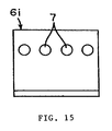
FIG. 15 illustrates the side of the terminal member 6i provided for the
monolithic ceramic capacitor 1i of FIG. 14 which faces an external electrode 2;
FIG. 16 is a perspective view of a monolithic ceramic capacitor 101 according
to an eleventh embodiment of the present invention;
FIG. 17 illustrates the positional relationship between the terminal elements
106 to 110 in the width direction of the external electrode 102, with respect to the
capacitor body 103 as shown in FIG. 16, and moreover, a displacement distribution of
the capacitor body 103 in the width direction of the external electrode 102, caused by
electrostriction;
FIG. 18, given to explain changing the sizes in the width direction of plural
terminal elements, is a side view showing the positional relationship between an
external electrode 112 formed on a capacitor body 111 and terminal elements 113 and
114;
FIG. 19, given to explain changing the intervals between adjacent ones of the
plural terminal elements, is a side view showing the positional relationship between
terminal elements 115 through 118 and an external electrode 112 on the capacitor
body 111;
FIG. 20 is a perspective view of a monolithic ceramic capacitor 101a
according to a twelfth embodiment of the present invention;
FIG. 21 is a perspective view partially showing a monolithic ceramic capacitor
101b according to a thirteenth embodiment of the present invention;
FIG. 22 is a perspective view of a monolithic ceramic capacitor 101c
according to a fourteenth embodiment of the present invention;
FIG. 23 is a perspective view of a monolithic ceramic capacitor 101d
according to a fifteenth embodiment of the present invention;
FIG. 24 is a perspective view of a monolithic ceramic capacitor 101e
according to a sixteenth embodiment of the present invention;
FIG. 25 is a partially sectional front view of a monolithic ceramic capacitor
101f according to a seventeenth embodiment of the present invention;
FIG. 26 is a perspective view partially showing the capacitor body 103 and the
terminal member 105f provided for the monolithic ceramic capacitor 101f of FIG. 25;
and
FIG. 27 is a side view of a monolithic ceramic capacitor according to an
eighteenth embodiment of the present invention.
DESCRIPTION OF PREFERRED EMBODIMENTS OF THE INVENTION
FIGS. 1 and 2 illustrate a monolithic ceramic capacitor according to a first
embodiment of the present invention. FIG. 1 is a front view, and FIG. 2 is a
perspective view.
The monolithic ceramic capacitor 1 contains a dielectric such as barium
titanate type ceramic, and at the opposite end faces, external electrodes 2 are formed,
respectively. The monolithic ceramic capacitor 1 is provided with a chip capacitor
body 4 in which plural internal electrodes 3 (see FIG. 3) are formed in lamination so
that each one is electrically connected to a predetermined one of the external
electrodes 2, and is further provided with terminal members 6 each formed of a metal
plate bonded to the external electrodes 2 by use of solder 5 as a conductive bonding
material.
In such a monolithic ceramic capacitor 1, in this embodiment,
characteristically, each terminal member 6 has a protuberance 7 formed so as to
project toward the external electrode 2, and the bonding portion 8 of the terminal
member 6 bonded to the external electrode 2 by use of the solder 5 is formed so as to
be elongated substantially linearly across a part of the external electrode 2.
In particular, each bonding portion 8 as described above is elongated
substantially linearly in parallel to the direction in which the internal electrodes 3
(FIG. 3) are extended. The protuberance 7 for forming the bonding portion 8 which
is elongated substantially linearly is also formed so as to be elongated continuously
linearly. More concretely, the protuberance 7 is formed of a bending line provided in
the metal plate constituting the terminal member 6. The bonding portion 8 is
provided, for example, by forming a solder film on the external electrode 2 previously,
and melting the solder film while the terminal member 6 is in contact with the solder
film, whereby the bonding portion 8 is formed so as to have a fillet generated by the
shrinkage of the solder caused by the surface tension. Further, the bonding portion 8
does not go all the way across the external electrode 2. That is, the size of the
bonding portion 8 in the longitudinal direction (the size in the direction perpendicular
to the plane of FIG. 1) is shorter than the size of the end-face of the capacitor body 4
in the same direction (the size in the direction perpendicular to the plane of FIG. 1).
This is one of measures which relax as much as possible the thermal shock that is
generated during soldering with solder 5.
Fig. 3 illustrates the displacement distribution between a pair of internal
electrodes 3 which is caused by electrostriction. FIG. 4 is an enlarged view of part of
the monolithic ceramic capacitor 1 of FIG. 1.
As seen in FIG. 3, the displacement caused by the electrostriction increases
with distance from the center line C1 between a pair of the internal electrodes 3.
Therefore, considering the whole of the capacitor body 4 in which plural layers of
such internal electrodes 3 are laminated, the displacement most likely to be caused by
the electrostriction is displacement in a thickness mode, as indicated by arrow 9 in
FIG. 4.
In this embodiment, the bonding portion 8 of the terminal member 6 and the
external electrode 2 lies along only a limited part of the external electrode 2, and is
elongated substantially linearly in parallel to the direction in which the internal
electrodes 3 are extended. Therefore, the displacement in a thickness mode caused by
the electrostriction as described above, not constrained substantially by the terminal
member 6, is transmitted to both the main faces 10 of the capacitor body 4, and the
energy of such displacement is effectively emitted from both the main faces 10 which
are free ends of the capacitor body 4, as indicated by arrow 11.
Accordingly, all of the bonding portion 8, the capacitor body 4, and moreover,
a wiring substrate (not illustrated) having the terminal member 6 soldered thereto can
be substantially prevented from being affected by such a stress caused by the
electrostriction as described above.
For the purpose of relaxing a stress caused by electrostriction based on the
above-described principle, it is preferable that the protuberance 7 of the terminal
member 6 is disposed as near to the center line C in the thickness direction of the
capacitor body 4 as possible, as shown in FIG.4, and the center in the width direction
of the bonding portion 8 formed of the solder 5 is positioned as near to the center line
C as possible. In relation to this, the distance a between the center in the width
direction of the bonding portion 8 and one-side edge of the end-face of the capacitor
body 4 in the lamination direction (the thickness direction of the capacitor body 4) of
the internal electrodes 3 is in the range of preferably 1/5 to 4/5, more preferably 2/8 to
6/8, and most preferably 3/8 to 5/8 of the size b of the end face of the capacitor body
4, the size b being measured in the lamination direction of the internal electrodes 3.
Similarly, for the purpose of relaxing a stress caused by the electrostriction, it
is preferable that the width c of the bonding portion 8 is as short as possible. In
relation to this, the width c of the bonding portion 8 is selected to be preferably up to
2/3, more preferably up to 4/9, still more preferably up to 1/3 of the size b of the end-face
of the capacitor body 4, the size being measured in the lamination direction of the
internal electrodes 3.
FIGS. 5, 6, 7, and 8 are partial front views showing monolithic ceramic
capacitors 1a, 1b, 1c, and 1d according to a second, a third, a fourth, and a fifth
embodiment of the present invention, respectively. Elements shown in FIGS. 5
through 8 equivalent to those in FIG. 1 are designated by similar reference numerals.
Duplicated description is omitted.
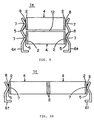
In a monolithic ceramic capacitor 1a as shown in FIG. 5, a protuberance 7 is
formed by the tip of a bent-portion of a terminal member 6a.
In a monolithic ceramic capacitor 1b as shown in FIG. 6, a protuberance 7 is
formed by a C-shaped bent-portion of a terminal member 6b.
In a monolithic ceramic capacitor 1c as shown in FIG. 7, a protuberance 7 is
formed by part of a loop-shaped bent-portion of a terminal member 6c.
In a monolithic ceramic capacitor 1d as shown in FIG. 8, the protuberance 7
of a terminal member 6d is not so sharp as that in FIG. 1 but has a predetermined
width.
FIGS. 9, 10, and 11 illustrate monolithic ceramic capacitors 1e, 1f, and 1g
according to a sixth, a seventh, and an eighth embodiment of the present invention,
respectively. FIGS. 9 and 10 are front views, and FIG. 11 is a perspective view.
Elements shown in FIGS. 9 through 11 equivalent to those in FIG. 1 are designated
by similar reference numerals. Duplicated description is omitted.
A monolithic ceramic capacitor 1e as shown in FIG. 9 has a stack component
structure in which plural, e.g., two capacitor bodies 4 are stacked and mounted
together by terminal members 6e which are attached to the respective external
electrodes 2 of the two capacitor bodies 4 in common. With these terminal members
6e, the two capacitor bodies 4 are electrically connected in parallel. The terminal
members 6e have protuberances 7 formed correspondingly to the external electrodes
2.
A gap 12 is provided between the two capacitor bodies 4 in order to prevent
the electrostriction phenomena occurring in the respective capacitor bodies 4 from
interfering with each other. The two capacitor bodies 4 may be bonded to each other
by use of an adhesive such as an adhesive with a Shore A hardness of up to 90 which
is capable of absorbing the electrostriction phenomenon, instead of the gap 12.
A monolithic ceramic capacitor 1f as shown in FIG. 10 is provided with plural,
e.g., two capacitor bodies 4 which are arranged in series so as to lie in a plane. The
external electrodes 2 of the respective two capacitor bodies 4 to be connected to each
other are bonded by use of a conductive bonding material such as solder or a
conductive adhesive. An appropriate terminal member preferably having a
protuberance, though not illustrated, may be inserted between the external electrodes
2 and bonded with the conductive bonding material, if necessary.
Terminal members 6f are attached to the external electrodes 2 positioned at
opposite ends of the two capacitor bodies 4 electrically connected in series,
respectively. The terminal members 6f have substantially the same shape as the
terminal members 6 as shown in FIG. 1.
A monolithic ceramic capacitor 1g as shown in FIG. 11 is provided with
plural, e.g., two capacitor bodies 4, which are arranged in parallel so as to lie in a
plane. These two capacitor bodies 4 are bonded by use of a two-sided pressure-sensitive
adhesive tape or an adhesive.
Terminal members 6g each have such a length that the respective external
electrodes 2 of the two capacitor bodies 4 can be connected in common.
FIG. 12 is a front view of a monolithic ceramic capacitor 1h according to a
ninth embodiment of the present invention, in which a part of the monolithic ceramic
capacitor is illustrated in a cross section. Elements in FIG. 12 equivalent to those in
FIG. 1 are designated by similar reference numerals, and the duplicated description is
omitted.
Characteristically, the monolithic ceramic capacitor 1h of FIG. 12 is provided
with a case 13 for accommodating a capacitor body 4 while terminal members 6h
partially project outside. In the perspective view of FIG. 13, only the components
which are accommodated in the case 13 of the monolithic ceramic capacitor 1h are
illustrated.
The terminal members 6h each are provided with plural, e.g., three comb-teeth
shape pieces 14. Protuberances 7 are formed in the comb-teeth shape pieces 14,
respectively. That is, in this embodiment, the plural protuberances 7 are formed in
each terminal member 6h so as to be distributed substantially linearly.
Further, positioning pieces 15 are integrally formed at both sides of the
terminal member 6h. The positioning pieces 15 are provided to position the capacitor
body 4 in the case 13, as seen most clearly in FIG. 12.
In this embodiment, the capacitor body 4 is covered with the case 13.
Therefore, the transmission of impact to the capacitor body 4 produced during
mounting can be reduced, and moreover, breaking of the capacitor body 4 caused by
collision with external objects can be prevented. In addition, an undesired stress
applied to the terminal member 6h can be prevented from being propagated to the
bonding portion 8.
Further, in this embodiment, though not illustrated, the space inside the case
13 may be packed with an appropriate resin (potting material). By this means, the
inside of the case 13 is shielded from moisture, gases, and so forth, and further
improvements in reliability are realizable. When high frequency current is applied to
the monolithic ceramic capacitor 1h, heat is generated due to the impedance of the
capacitor body 4. However, by employing a potting resin having a high thermal
conductivity, the heat radiation efficiency can be enhanced, as compared with the
instance where a space remains in the case 13.
FIG. 14 is a front view of a monolithic ceramic capacitor 1i according to a
tenth embodiment of the present invention. Elements in FIG. 14 equivalent to those
in FIG. 1 are designated by similar reference numerals, and duplicated description is
omitted.
The monolithic ceramic capacitor 1i as shown in FIG. 14 is provided with
terminal members 6i only one of which is shown in FIG. 15. FIG. 15 illustrates the
side of the terminal member 6i which faces the external electrode 2. The terminal
member 6i is provided with plural protuberances 7 distributed substantially linearly.
These protuberances 7 can be formed by deep drawing by means of a press when the
terminal member 6i is shaped.
As in the previous embodiments, also in the instance of plural protrusions 7
provided so as to be distributed substantially linearly as in this embodiment, the
bonding portion 8 for bonding to an external electrode 2, formed of a solder 5, can be
distributed substantially linearly across a part of the external electrode 2.
The present invention has been described in reference to the illustrated several
embodiments. In addition, various modifications and variations are possible without
departing from the scope of the present invention.
For example, in the above-described embodiments, the solder 5 is used as the
conductive bonding material for bonding the terminal members 6 or the like to the
external electrodes 2. A conductive adhesive may be employed instead of the solder
5. Moreover, when the solder 5 is employed, the advantages of the present invention
become more prominent by using solder having a relatively high hardness such as
lead-free solder.
Further, in the above-described embodiments, the bonding portion 8 is formed
so as to be elongated linearly along one straight line. However, the bonding portion 8
may be formed so as to be elongated along at least two straight lines or along a
curved line.
Moreover, in the above-described embodiments, only the bonding portion 8 is
formed with the solder 5. However, solder may be applied to other areas of the
terminal members 6 or the like, and the external electrodes 2, in other places besides
the bonding portion 8. For example, solder may be coated all over the surface of an
external electrode 2 or a terminal member 6.
In addition, an embodiment in which the features of the respective
embodiments described above are combined is possible. For example, the structure
containing the case 13 as shown in FIG. 12 may be employed in the respective
embodiments as shown in FIGS. 1, 5 through 11, and 14. Moreover, in the respective
embodiments of FIGS. 9 through 11 containing plural capacitor bodies 4, the shapes
of the terminal members as shown in FIG. 5 through 8, 12, and 14 may be employed.
Further, the terminal members 6h as shown in FIG. 12 may be applied to a monolithic
ceramic capacitor not provided with the case 13.
FIG. 16 is a perspective view of a monolithic ceramic capacitor 101 according
to an eleventh embodiment of the present invention.
The monolithic ceramic capacitor 101 is provided with external electrodes 102
formed at the opposite end faces thereof, a chip capacitor body 103 in which plural
internal electrodes (not illustrated) are formed in lamination so as to be electrically
connected to a predetermined one of the external electrodes 102, respectively, and
terminal members 105 each formed of a metal plate bonded to the external electrodes
102 by use of solder 104 as a conductive bonding material.
In such a monolithic ceramic capacitor 101, in this embodiment, each terminal
member 105 comprises plural, e.g., five terminal elements 106, 107, 108, 109, and
110 arranged so as to be distributed at intervals in the width direction of the external
electrode 2. These terminal elements 106 through 110 are so constructed that the
terminal elements 106 and 110 positioned at the ends in the arrangement direction
have a lower constraining-degree than the terminal element 108 or the terminal
elements 107 through 109 positioned in the center, said constraining degree being
defined as the degree of constraining a stress produced by the electrostriction
phenomenon in the capacitor body 103, which is attributed to the bonding of the
terminal elements 106 through 110 to the external electrode 102.
More concretely, in the terminal elements 106 through 110, the terminal
elements positioned at the ends in the arrangement direction have a smaller bonding
area on the external electrode 102, as compared with the terminal elements positioned
in the center. Still more concretely, as compared with the terminal elements 108 or
the terminal elements 107 through 109 positioned in the center, the terminal elements
106 and 110 positioned at the ends in the arrangement direction have a smaller size in
the width direction, and moreover, the intervals between the terminal elements 106
and 110 and the corresponding next terminal elements 107 and 109 are wider than
those between the terminal element 108 at the center and the next terminal elements
107 and 109.
FIG. 17 shows the position relationship of the terminal elements 106 through
110 to the capacitor body 103 in the width direction of the external electrode 102. In
addition, illustrated is the displacement distribution in the width direction of the
external electrode 102 of the capacitor body 103 caused by electrostriction.
When the electrostriction in an area mode is generated in the monolithic
ceramic capacitor 101, the displacement ratio of the capacitor body 103, observed in
the width direction of the external electrode 102, is zero at the center, and becomes
larger at a position farther from the center, as shown in FIG. 17.
Accordingly, as described above, referring to the degree of constraining a
stress produced by the electrostriction phenomena of the capacitor body 103, which is
attributed to the bonding of the plural terminal elements 106 through 110 to the
external electrode 102, the terminal elements 106 and 110 positioned at the ends
where a high displacement ratio is caused by the electrostriction can be adjusted to
have a lower constraining-degree than those of the terminal elements 108 or the
terminal elements 107 through 109 positioned in the center where a low displacement
ratio is caused by the electrostriction by setting the size in the width direction of the
terminal elements 106 and 110 positioned at the ends to be smaller than that of the
terminal element 108 or 107 through 109 positioned in the center, and moreover,
setting the intervals between the terminal elements 106 and 110 positioned at the ends
and the corresponding next terminal elements 107 and 109 to be wider than those
between the terminal element 108 positioned at the center and the next terminal
elements 107 and 109.
As a result, the effects of stress caused by electrostriction on the bonding
portions of the terminal elements 106 through 110 bonded to the external electrodes
102 with solder 104, the capacitor body 103, and a wiring substrate (not illustrated)
having the terminal elements 106 through 110 soldered thereto, can be reduced.
Thus, the above-described embodiment, can reduce the degree of constraint of
a stress produced by the electrostriction phenomenon in the capacitor body 103,
which is attributed to the bonding of the terminal elements 106 through 110 to the
external electrode 102. Two means are employed for reducing the constraining-degree
of the terminal elements positioned at the ends in the arrangement direction of
the plural terminal elements 106 through 110, to be lower than that of the terminal
elements positioned in the center; first, changing the sizes in the width direction of the
terminal elements 106 through 110, and second, changing the intervals between the
terminal elements 106 through 110. Either one or both of these two means may be
employed. This will be described below with reference to FIGS. 18 and 19.
FIG. 18, given to explain changing the sizes in the width direction of the
terminal elements, illustrates the positional relationship between the external electrode
112 on the capacitor body 111 and the terminal elements 113 and 114.
Referring to FIG. 18, the size in the width direction of the terminal element
113 positioned at the end is designated by W1, and that of the terminal element 114
positioned at the center by W2. All of the intervals between adjacent terminal
elements of the plural terminal elements containing the terminal elements 113 and 114
are assumed to be equal, though not illustrated.
In such a monolithic ceramic capacitor, the ratio of the size W1 in the width
direction of the
terminal element 113 at the end to the size W2 of the
terminal element
114 at the center was varied as listed in the following Table 1, and for each case, the
generation ratio of cracks was measured. The crack generation ratio is a ratio at
which cracks are generated in the
capacitor body 111 when a high frequency current
is applied.
| W1 | CRACK GENERATION RATIO |
| W2 x 1 | 5 % |
| W2 x 0.9 | 0.5 % |
| W2 x 0.8 | 0 % |
| W2 x 0.7 | 0 % |
| W2 x 0.6 | 0 % |
As seen in Table 1, the crack generation ratio can be reduced by setting the size W1
in the width direction of the terminal element 113 positioned at the end to be smaller
than the size W2 in the width direction of the terminal element 114 at the center. For
example, the generation of cracks can be reliably prevented by setting the size W1 in
the width direction to be smaller than the size W2 in the width direction multiplied by
0.8.
FIG. 19, given to explain changing the intervals between adjacent ones of the
plural terminal elements, is a side view illustrating the positional relationship between
the external electrode 112 on the capacitor body 111 and the terminal elements 115
through 118.
Hereupon, shown is the positional relationship of the interval G1 between the
terminal element 115 at the end and the next terminal element 116 to the interval G2
between the terminal element 118 at the center and the next terminal element 117.
The sizes in the width direction of the terminal elements 115 through 118 are set to be
equal.
The following Table 2 lists the crack generation ratios which were obtained
when the ratio of the interval G1 between the
terminal element 115 at the end and the
terminal element 116 to the interval G2 between the
terminal element 118 at the
center and the
terminal element 117 was varied.
| G1 | CRACK GENERATION RATIO |
| G2 x |
| 1 | 5 % |
| G2 x 1.1 | 0.6 % |
| G2 x 1.2 | 0 % |
| G2 x 1.3 | 0 % |
| G2 x 1.4 | 0 % |
As seen in Table 2, the crack generation ratio can be reduced by setting the
interval G1 between the terminal element 115 positioned at the end and the terminal
element 116 to be wider than the interval G2 between the terminal element 117
positioned at the center and the terminal element 118. In particular, the generation of
cracks can be reliably prevented by setting the interval G1 to be more than the interval
G2 multiplied by 1.2.
FIGS. 20 and 21 are perspective views partially illustrating monolithic ceramic
capacitors 101a and 101b according to twelfth and thirteenth embodiments of the
present invention, respectively. Elements in FIGS. 20 and 21 equivalent to elements
shown in FIG. 16 are designated by similar reference numerals. Duplicated
description is omitted.
In each terminal member 105 of FIG. 16, the plural terminal elements 106
through 110 are independent of each other. In the terminal members 105a and 105b
as shown in FIGS. 20 and 21, respectively, the plural terminal elements 106 through
110 are formed in a comb-teeth shape.
Further, in the terminal member 105b of FIG. 21, the terminal elements 106
through 110 each have a bending shape to form a line-shaped or point-shaped
bonding portion on the external electrode 102.
FIGS. 22, 23, and 24 are perspective views showing monolithic ceramic
capacitors 101c, 101d, and 101e according to a fourteenth, a fifteenth, and a sixteenth
embodiment of the present invention, respectively. Elements in FIGS. 22 through 24
equivalent to those in FIG. 16 are designated by similar reference numerals.
Duplicated description is omitted.
The monolithic ceramic capacitor 101c as shown in FIG. 22 has a stack
component shape in which plural, e.g., two capacitor bodies 103 are stacked and
attached together by a terminal member 105c comprising plural terminal elements 106
through 110 which is attached to the respective external electrodes 102 of the two
capacitor bodies 103 in common. With the terminal members 105c, the two capacitor
bodies 103 are electrically connected in parallel.
A gap 119 is provided between the two capacitor bodies 103 to prevent the
electrostriction phenomena occurring in the respective capacitor bodies 103 from
interfering with each other. The two capacitor bodies 103 may alternatively be
bonded to each other through an adhesive with a Shore A hardness of up to 90
instead of the gap 119.
The monolithic ceramic capacitor 101d as shown in FIG. 23 is provided with
plural, e.g., two capacitor bodies 103. These capacitor bodies 103 are arranged in
series so as to lie in a plane. The external electrodes 102 to be connected of the two
capacitor bodies 103 are bonded to each other though a conductive bonding material
such as solder, a conductive adhesive, or the like. An appropriate terminal member,
though not illustrated, may be inserted between the external electrodes 102 and
bonded though the conductive bonding material, if necessarily.
Terminal members 105d composed of plural terminal elements 106 through
110 are attached to the external electrodes 102 positioned at the opposite ends of the
two capacitor bodies 103 electrically connected in series as described above,
respectively.
The monolithic ceramic capacitor 101e as shown in FIG. 24 is provided with
plural, e.g., two capacitor bodies 103. These capacitor bodies 103 are arranged in an
array component form in which the capacitor bodies 103 are arranged in parallel so as
to lie in a plane and connected together. These two capacitor bodies 103 are bonded
to each other by use of a two-side pressure-sensitive tape or an adhesive.
Terminal members 105e each composed of plural terminal elements 106
though 110 are attached to the external electrodes 102 of the two capacitor bodies
103, respectively.
FIG. 25 is a sectional, front partial view showing a monolithic ceramic
capacitor 101f according to a seventeenth embodiment of the present invention.
Elements in FIG. 25 equivalent to those in FIG. 16 are designated by similar reference
numerals. Duplicated description is omitted.
Characteristically, the monolithic ceramic capacitor 101f as shown in FIG. 25
is provided with a case 120 for accommodating a capacitor body 103 while terminal
members 105f are partially exposed outside. The perspective view of FIG. 26, is only
a partial view of the components accommodated in the case 120 of the monolithic
ceramic capacitor 101f.
In each terminal member 105f, plural terminal elements 106 though 110 are
formed in a comb-teeth shape similarly to the terminal member 105b as shown in FIG.
21, and moreover, the terminal elements 106 though 110 are bent, respectively.
Further, positioning pieces 121 are integrally provided for each terminal
member 105f at both sides thereof. The positioning pieces 121 are provided to
position the capacitor body 103 in the case 120, as seen most clearly in FIG. 25.
In this embodiment, the capacitor body 103 is covered with the case 120. The
transmission of impact during mounting to the capacitor body 103 can be reduced,
and moreover, breaking of the capacitor body 103 caused by collision with external
objects can be prevented. In addition, the case 120 can prevent an undesired stress
applied to the terminal member 105f from being propagated to the bonding portion
formed with solder 104.
Further, in this embodiment, though not illustrated, the space inside the case
120 may be packed with an appropriate resin (potting resin). By this way, the inside
of the case 120 is shielded from moisture, gases, and so forth, and further
improvements in reliability are realizable. When high voltage or high frequency
current is applied to the monolithic ceramic capacitor 101f, heat is generated due to
the impedance of the capacitor body 103. However, when a resin having a high
thermal conductivity is employed as a potting resin, the heat radiating efficiency can
be enhanced, as compared with the instance where the space remains in the case 120.
Heretofore, the present invention has been described in relation to the several
illustrated embodiments. Further, various modifications and variations are possible
without departing from the scope of the present invention.
For example, in the above-described embodiments, as the conductive bonding
material for bonding the terminal members 105 or the like to the external electrodes
102, the solder 104 is used. However, conductive adhesive may be employed.
Further, in the illustrated embodiments, the solder 104 is coated all over the
surface of the external electrodes 102. However, the solder 104 may be applied only
to the portion required for the bonding to the terminal members 105 or the like.
In addition, an embodiment is possible in which the respective features of the
above-described embodiments are combined. For example, the construction in which
the case 120 as shown in FIG. 25 is provided may be employed in the respective
embodiments as shown in FIGS. 16, and 20 through 24. Moreover, in the
embodiments each containing the plural capacitor bodies 103 as shown in FIGS. 22
through 24, the shapes of a terminal member as shown in FIGS. 19, 20, and 21,
respectively may be employed.
In the respective embodiments described above, in order that the size in the
width direction of the respective terminal elements 106 and 110 is adjusted to be
smaller than that of the respective terminal elements 107 through 109, the overall size
in the width direction of the respective terminal elements 106 and 110 is decreased.
Instead of this, in a respective part of each of the terminal elements 106 and 110, and
more concretely, only in the respective parts thereof bonded to the external electrode
102, a notch or the like may be provided to reduce the size in the width direction.
In the above-described respective embodiments, as to the bonding areas of the
plural terminal elements 106 through 110 bonded to the external electrode 102,
effects of a stress caused by the electrostriction are reduced by making the bonding
areas of the terminal elements at the ends in the width direction of the external
electrode 102 smaller than those of the terminal elements in the center. Instead of
this, the thickness of the terminal elements positioned at the ends in the arrangement
direction may be thinner than that of the terminal elements positioned in the center so
that the degree of constraining a stress caused by the electrostriction is reduced.
For example, as shown in Fig. 27, when the width W3 of an internal electrode
is wider than the width W4 of the terminal member, damage to the ceramic, caused by
electrostriction, can be more inhibited, since it suffers no effects of the gap portion
between the internal electrode and an outer layer which is a non-vibrating portion.
As described above, according to the present invention, terminal members
each bonded to an external electrode of a capacitor body through a conductive
bonding material are provided with a protrusion projecting toward the external
electrode, and thereby, the bonding portion of the terminal member bonded to the
external electrode, formed with the conductive bonding material is elongated
substantially linearly on a part of the external electrode. Accordingly, electrostriction
phenomena in the capacitor body are scarcely constrained, so that a stress caused by
the electrostriction can be relaxed. Accordingly, breaking of the bonding portion and
cracking of the capacitor body, and so forth, caused by such a stress, can be
advantageously prevented. In addition, "creaking" can be considerably reduced.
In a capacitor body having plural internal electrodes formed in lamination
therein, electrostriction in a thickness mode, that is, in the perpendicular to the
internal electrodes is generated most readily. Accordingly, when the direction in
which the bonding portion is elongated substantially linearly is substantially in parallel
to the direction in which the internal electrodes are extended, vibration caused by
electrostriction is scarcely constrained by the bonding portion of the terminal member,
but is effectively emitted through the free ends of the capacitor body. Thus, the
relaxation of a stress caused by electrostriction can be achieved more effectively.
Moreover, when the width of the bonding portion is selected to be preferably
up to 2/3, more preferably up to 4/9, and most preferably up to 1/3 of the size of the
end face of the capacitor body, the size being measured in the lamination direction of
the internal electrodes, the effect on the relaxation of a stress generated by
electrostriction as described above can be achieved more securely.
Further, when the center in the width direction of the bonding portion is
positioned in the range of 1/5 to 4/5, more preferably 2/8 to 6/8, and still more
preferably 3/8 to 5/8 of the size of the end face from one side edge of the end face of
the capacitor body in the lamination direction of the internal electrodes, the size being
measured in the lamination direction of the internal electrodes, the effect on the
relaxation of a stress generated by the electrostriction can be achieved more reliably
as in the above instance.
According to the present invention, when the structure is employed in which
plural capacitor bodies are provided, and terminal members are attached to the
respective external electrodes of the capacitor bodies in common, the terminal
members can function as a conductive member for connecting the plural capacitor
bodies in parallel, for example. Accordingly, for example, a stack component can be
simply obtained.
Furthermore, in the present invention, when the structure with the case for
accommodating a capacitor body is employed, an impact produced during mounting is
hardly transmitted to the capacitor body, and breaking of the capacitor body caused
by collisions with external objects can be prevented. In addition, an undesired stress
applied to a terminal member can be prevented from being propagated to the bonding
portion.
When the case is provided as described above, and the positioning piece for
positioning a capacitor body in the case is formed integrally with a terminal member,
the capacitor body can be easily positioned without addition of a special piece for
positioning, assembly of the monolithic ceramic capacitor can be simply carried out,
and breaking of the monolithic ceramic capacitor in the mounting state can be
advantageously prevented.
As described above, according to the present invention, a terminal member is
provided with plural terminal elements arranged so as to be distributed at intervals in
the width direction of an external electrode. The plural terminal elements, are
constructed so that as to set the degree of constraining a stress produced by the
electrostriction phenomenon in a capacitor body, which is attributed to the bonding of
the terminal elements to the external electrode. More specifically, each terminal
element positioned at the ends in the arrangement direction has a lower constraining-degree
than each terminal element positioned in the center. Accordingly, on the
portions where the terminal members are bonded to the external electrodes, on the
capacitor body, and so forth, effects of a stress caused by electrostriction can be
reduced. As a result, breaking of the bonding portions and cracking in the capacitor
body, and so forth can be advantageously prevented.
According to the present invention, the desired degree of constraint can be
simply realized, by setting the plural terminal elements at the ends in the width
direction of the external electrode so as to have a smaller bonding area on the external
electrode, as compared with the bonding area in the center.
In particular, the degree of constraining a stress as described above can be
desirably realized by a simpler method by setting the plural terminal elements so that
the size in the width direction of each terminal element positioned at the ends in the
arrangement direction is smaller than each terminal element positioned in the center,
and/or by setting the plural terminal elements so that the intervals between the
terminal elements positioned at the ends in the arrangement direction and the next
terminal elements are longer than those between the terminal element positioned in
the center and the next terminal elements.
According to the present invention, the plural terminal elements may have the
form that they are independent of each other or the terminal members each may have
the plural terminal elements formed in a comb-teeth shape. These plural terminal
elements can be simply obtained by changing suitably the cutting position of a
material, for example, a hoop material, prepared for production of the terminal
members.
When the structure is employed in which the capacitor body is accommodated
in the case according to the present invention, impact during mounting is hardly
transmitted to the capacitor body, breaking of the capacitor body caused by collision
with external objects can be prevented, and moreover, an undesired stress applied to a
terminal member can be prevented from being propagated to the bonding portions of
the terminal member bonded to the external electrode.
In the instance that the case is provided as described above, by forming a
positioning piece for positioning the capacitor body in the case integrally with the
terminal member, the capacitor body can be easily positioned without addition of a
special piece for positioning, assembly of the monolithic ceramic capacitor can be
easily carried out, and breaking of the monolithic ceramic capacitor in the mounting
state can be advantageously prevented.
Although the present invention has been described in relation to particular
embodiments thereof, many other variations and modifications and other uses will
become apparent to those skilled in the art. Therefore, the present invention is not
limited by the specific disclosure herein.