EP1012966B1 - Appareil et procede d'estimation de phase par blocs - Google Patents
Appareil et procede d'estimation de phase par blocs Download PDFInfo
- Publication number
- EP1012966B1 EP1012966B1 EP97947437A EP97947437A EP1012966B1 EP 1012966 B1 EP1012966 B1 EP 1012966B1 EP 97947437 A EP97947437 A EP 97947437A EP 97947437 A EP97947437 A EP 97947437A EP 1012966 B1 EP1012966 B1 EP 1012966B1
- Authority
- EP
- European Patent Office
- Prior art keywords
- phase
- circuit
- coupled
- input
- measurement
- Prior art date
- Legal status (The legal status is an assumption and is not a legal conclusion. Google has not performed a legal analysis and makes no representation as to the accuracy of the status listed.)
- Expired - Lifetime
Links
- 238000000034 method Methods 0.000 title claims description 12
- 238000012935 Averaging Methods 0.000 claims description 27
- 238000005259 measurement Methods 0.000 claims 23
- 230000001131 transforming effect Effects 0.000 claims 4
- 238000001914 filtration Methods 0.000 claims 2
- 238000010586 diagram Methods 0.000 description 11
- 239000000523 sample Substances 0.000 description 11
- 239000013598 vector Substances 0.000 description 9
- 230000003111 delayed effect Effects 0.000 description 4
- 230000008859 change Effects 0.000 description 2
- 230000001934 delay Effects 0.000 description 2
- 238000005516 engineering process Methods 0.000 description 2
- 230000010363 phase shift Effects 0.000 description 2
- 230000008569 process Effects 0.000 description 2
- 230000001360 synchronised effect Effects 0.000 description 2
- 230000009466 transformation Effects 0.000 description 2
- 230000008901 benefit Effects 0.000 description 1
- 230000005540 biological transmission Effects 0.000 description 1
- 230000001413 cellular effect Effects 0.000 description 1
- 238000006243 chemical reaction Methods 0.000 description 1
- 230000001427 coherent effect Effects 0.000 description 1
- 238000004891 communication Methods 0.000 description 1
- 238000010276 construction Methods 0.000 description 1
- 238000012937 correction Methods 0.000 description 1
- 238000001514 detection method Methods 0.000 description 1
- 238000012986 modification Methods 0.000 description 1
- 230000004048 modification Effects 0.000 description 1
- 239000013074 reference sample Substances 0.000 description 1
- 238000005316 response function Methods 0.000 description 1
- 238000005070 sampling Methods 0.000 description 1
- 238000009738 saturating Methods 0.000 description 1
- 238000004088 simulation Methods 0.000 description 1
Images


Classifications
-
- H—ELECTRICITY
- H04—ELECTRIC COMMUNICATION TECHNIQUE
- H04L—TRANSMISSION OF DIGITAL INFORMATION, e.g. TELEGRAPHIC COMMUNICATION
- H04L27/00—Modulated-carrier systems
- H04L27/18—Phase-modulated carrier systems, i.e. using phase-shift keying
- H04L27/22—Demodulator circuits; Receiver circuits
- H04L27/233—Demodulator circuits; Receiver circuits using non-coherent demodulation
- H04L27/2332—Demodulator circuits; Receiver circuits using non-coherent demodulation using a non-coherent carrier
-
- H—ELECTRICITY
- H03—ELECTRONIC CIRCUITRY
- H03D—DEMODULATION OR TRANSFERENCE OF MODULATION FROM ONE CARRIER TO ANOTHER
- H03D3/00—Demodulation of angle-, frequency- or phase- modulated oscillations
- H03D3/006—Demodulation of angle-, frequency- or phase- modulated oscillations by sampling the oscillations and further processing the samples, e.g. by computing techniques
-
- H—ELECTRICITY
- H03—ELECTRONIC CIRCUITRY
- H03D—DEMODULATION OR TRANSFERENCE OF MODULATION FROM ONE CARRIER TO ANOTHER
- H03D3/00—Demodulation of angle-, frequency- or phase- modulated oscillations
- H03D3/007—Demodulation of angle-, frequency- or phase- modulated oscillations by converting the oscillations into two quadrature related signals
-
- H—ELECTRICITY
- H04—ELECTRIC COMMUNICATION TECHNIQUE
- H04L—TRANSMISSION OF DIGITAL INFORMATION, e.g. TELEGRAPHIC COMMUNICATION
- H04L27/00—Modulated-carrier systems
- H04L27/0014—Carrier regulation
- H04L2027/0024—Carrier regulation at the receiver end
- H04L2027/0026—Correction of carrier offset
- H04L2027/003—Correction of carrier offset at baseband only
-
- H—ELECTRICITY
- H04—ELECTRIC COMMUNICATION TECHNIQUE
- H04L—TRANSMISSION OF DIGITAL INFORMATION, e.g. TELEGRAPHIC COMMUNICATION
- H04L27/00—Modulated-carrier systems
- H04L27/0014—Carrier regulation
- H04L2027/0044—Control loops for carrier regulation
- H04L2027/0046—Open loops
-
- H—ELECTRICITY
- H04—ELECTRIC COMMUNICATION TECHNIQUE
- H04L—TRANSMISSION OF DIGITAL INFORMATION, e.g. TELEGRAPHIC COMMUNICATION
- H04L27/00—Modulated-carrier systems
- H04L27/0014—Carrier regulation
- H04L2027/0044—Control loops for carrier regulation
- H04L2027/0063—Elements of loops
- H04L2027/0067—Phase error detectors
-
- H—ELECTRICITY
- H04—ELECTRIC COMMUNICATION TECHNIQUE
- H04L—TRANSMISSION OF DIGITAL INFORMATION, e.g. TELEGRAPHIC COMMUNICATION
- H04L27/00—Modulated-carrier systems
- H04L27/0014—Carrier regulation
- H04L2027/0044—Control loops for carrier regulation
- H04L2027/0063—Elements of loops
- H04L2027/0069—Loop filters
Definitions
- the present invention relates to a phase averaging circuit for a phase estimator.
- Differential demodulator technology is often selected for a burst demodulator.
- a differential demodulator locks on to the carrier instantly; however, it has degraded performance in presence of noise.
- a coherent demodulator where the carrier is coherently regenerated using a filter or phase locked loop, will theoretically provide superior noise performance if the loop bandwidth is narrow relative to the symbol rate; however, it is comparatively slow to lock on to the carrier. In the case of a phase locked loop, the lock on time is further increased by a hang-up phenomenon.
- a block phase estimator is an alternative to the phase locked loop.
- the block phase estimator provides performance similar to the phase lock loop but does not suffer from the hang-up phenomenon.
- digital receiver 10 includes an antenna coupled to a receiver.
- the receiver's output from its IF final stage is provided to in-phase and quadrature mixers.
- a local oscillator using a Hilbert ( ⁇ /2) transformer, provides in-phase and quadrature phase reference signals to the mixers.
- the mixer outputs are analog in-phase signal I and analog quadrature phase signal Q.
- Analog signals I,Q are sampled in analog to digital converters, filtered, decimated and interpolated to produce digitally sampled signals I i and Q i .
- the filter is preferably a Nyquest filter matched to the modulation expected.
- the decimator/interpolator down samples the samples from the analog to digital converter to the symbol rate and resamples the signal at the center of each symbol.
- the outputs I i , Q i from digital receiver 10 do not vary with time. However, if the oscillator is tuned to a frequency other than the exact frequency of the signal being received, outputs I i , Q i will vary with time.
- the phase of the filtered/decimated/interpolated voltage V i is represented by the arctangent of the ratio of Q i to I i . This phase angle variation over time corresponds to the frequency difference between the oscillator's characteristic frequency and the frequency of the signal received at the antenna.
- phase-locked loop synchronous detectors measure this phase difference, filter the measured difference, and use this filtered phase difference to control the frequency of the local oscillator (i.e., a voltage controlled oscillator).
- the present invention relates to a block phase estimator as an alternative technology to phase-locked loops.
- a constant frequency received by digital receiver 10 has little or no utility since it carries no information.
- signals received by the antenna include modulation.
- the present invention relates to a block phase estimator used in a decoder for decoding phase shift keying (PSK).
- FIG. 2 is a graph depicting locations of voltage V from digital receiver 10 receiving a QPSK (quadrature phase shift keying) signal as received by both conventional decoders and a decoder according to the present invention.
- Signals I i , Q i may be plotted on the graph of FIG. 2.
- a symbol may take on one of four values depicted in FIG. 2 as -135° - 45° +45° +135°.
- the object of a decoder is to determine which phase is being transmitted during the duration of the symbol.
- conventional decoder 60 includes block phase estimator 50, and block phase estimator 50 includes modulation removal circuit 20, averager 30 and phase corrector tracker 40.
- FIG. 3 depicts modulation removal circuit 20.
- Modulation removal circuit 20 includes Cartesian to polar transformer 22, multiplier 24 and a polar to Cartesian transformer made from a cosine transformer 26 and a sine transformer 28.
- digital sample signals I i , Q i from digital receiver 10 (FIG. 1) are converted to polar coordinates using an arctangent function to provide a phase estimate of the phase of the current sample.
- the phase estimate of the phase of the current sample is phase ⁇ i .
- Multiplier 24 multiplies phase ⁇ i by M, where M is the number of phases encoded into the PSK signal. This provides a phase estimate of the current sample with modulation removed.
- multiplier 24 For BPSK signals, M is 2; for QPSK signals, M is 4; for 8-PSK signals, M is 8; etc.
- FIG. 2 depicts four phases so that M would equal 4; however, M may advantageously be 8, 16, etc.
- the output of multiplier 24 is converted back into Cartesian coordinates by cosine transformer 26 and sine transformer 28 to provide signals I i ', Q i '. It should be noted here that the output of multiplier 24 may include phase angles greater than 2 ⁇ radians; however, transformers 26, 28 are cyclical in nature and the outputs of these transformers are uneffected by angles greater than 2 ⁇ radians.
- modulation removal circuit 20 The operation of modulation removal circuit 20 is best understood in connection with FIG. 2.
- the four locations depicted in FIG. 2 as possible voltages from receiver 10 will become multiplied in multiplier 24 by four (4) since the signals depicted in FIG. 2 are quadrature PSK signals.
- the 45° phase depicted in the first quadrant in FIG. 2 when multiplied by 4 becomes 180°.
- the -45° when multiplied by four becomes -180°.
- the 135° phase angle becomes 540° (i.e., 180° + 360°).
- the -135° becomes -540°.
- cosine and sine transformers 26, 28 cyclically repeat, all phases output of multiplier 24 created from any one of the signal locations depicted in FIG. 2 will be interpreted as having a phase angle of 180°.
- modulation is removed by modulation removal circuit 20.
- the constellation of four locations depicted in FIG. 2 will rotate with time, either counter clock wise or clock wise depending on the sign of the frequency deviation. It is this frequency deviation that is measured in the block phase estimator. If there is a small frequency deviation, the phase output of multiplier 24 will be different than 180°.
- FIG. 4 depicts conventional averager 30 as having two separate averaging circuits 32.
- Each averaging circuit 32 provides average signals I AVG ', Q AVG ' by maintaining a moving average of the input signals I i ' Q i '.
- the averaging is carried out, preferably, over a duration of time corresponding to several symbols.
- the sampling rate of the A to D converters in FIG. 1 is higher than the symbol rate.
- the analog to digital converters may provide four samples over a symbol duration, and averaging circuits 32 would average the values input to these circuits by adding the values from sixteen samples and dividing by sixteen or scaling appropriately (e.g., four samples with four samples per symbol).
- phase corrector tracker 40 includes Cartesian to polar transformer 42 (similar to Cartesian to polar transformer 22 in FIG.3), divider 44, sector tracker 46, and polar to Cartesian transformer 48 (similar to the polar to Cartesian transformer 26, 28 of FIG. 3).
- Divider circuit 44 merely divides the phase input thereto (i.e., ⁇ AVG ') by M to provide the signal input to the sector tracker.
- Divider 44 restores the phase value that was multiplied in multiplier 24 of FIG. 3; however, the range over which the phase output of divider 44 may vary is limited to 360° ⁇ M.
- sector tracker 46 adds or subtracts a phase angle defined by 360° ⁇ M whenever it detects that the phase output of divider 44 jumps sharply. The output of sector tracker 46 is then converted to Cartesian coordinates in transformer 48.
- the output of block phase estimator 50 (FIG. 6) contains Cartesian values for I, Q with the modulation removed but averaged over the averaging interval (e,g., 4 symbols).
- the output of block phase estimator 50 is estimated reference signals I EST , Q EST .
- Signals I i , Qi are delayed in delay circuits 52 to provide delayed signals I DEL , Q DEL .
- the delay duration can be chosen to use prior symbols, post symbols, or a combination of both.
- De-rotator 54 is a full complex by complex multiplier to form the product of delayed incoming data signal I DEL , Q DEL with reference signal I EST , Q EST .
- the output of de-rotator 54 is passed to decision devices 56.
- the in-phase decision device output value indicates whether the voltage being detected is in the left or right half plane of the plane depicted in FIG. 2, and the quadrature decision device output value indicates whether the voltage being detected is in the upper or lower half plane of FIG. 2.
- Decision devices 56 may include two comparators to determine which half plane the I value is in and which half plane the Q value is in.
- US-A-5202901 describes a digital radio receiver for synchronization of radiowave transmissions for digital and analog FM signals in TDMA systems such as cellular telephones.
- the receiver uses a tangent type discriminator that is said to minimize the bit error rate.
- the digital discriminator employs an A/D converter circuit that samples a received intermediate frequency (IF) signal, a sorter circuit that produces a predetermined number of samples to be used in the decoding, a sample and phase adjustment circuit that allows for a carrier phase adjustment and sample timing adjustment, a divider circuit that eliminates the need for a conventional limiter by causing a ratio of amplitudes to be processed instead of absolute signal amplitudes, an inverse tangent circuit that creates a decoded phase angle from the ratio, a delay circuit and a summer circuit that create a differential signal, a modulo-2 ⁇ correction circuit that corrects for wrap-around errors about the real axis, an integrate and dump filter for summing up all phase angles pertaining to a single symbol, and a four-phase decoder circuit to decode the signal into a pair of bits.
- IF intermediate frequency
- An adjustment circuit minimizes phase error between a reference sequence of symbols and the decoded symbols by simultaneously adjusting the sample timing and carrier phase adjustments.
- the digital discriminator also can decode conventional analog FM radio broadcasts by deactivating the IDF, the adjustment circuit, and SPA circuit, and bypassing the four-phase decoder.
- An advantage of the present invention is that it may achieve phase averaging while avoiding a need to convert polar formatted data into Cartesian formatted data and back again.
- a first embodiment of the phase averaging circuit includes a phase differencing circuit coupled to an averager input, a first modulo circuit coupled to the phase differencing circuit, a filter coupled to the first modulo circuit, and a summation circuit having an positive input and a negative input, the positive input being coupled to the averager input, the negative input being coupled to the filter.
- the phase averaging circuit further includes a second modulo circuit coupled to the summation circuit.
- phase averaging circuit includes a delay line having a plurality of taps coupled to an averager input and a plurality of first subtractor circuits, a first input of each first subtractor circuit being coupled to the averager input, a second input of each first subtractor circuit being coupled to a corresponding first subtractor circuit.
- a summation circuit is coupled to all first modulo circuits, and a scaling circuit is coupled to the summation circuit.
- the phase averaging circuit further includes a second subtracter circuit, a first input of the second subtractor circuit being coupled to the averager input, a second input of the second subtractor circuit being coupled to the scaling circuit.
- the output of the arctangent transformation of a vector is the phase of the vector.
- the phase lies between - ⁇ and + ⁇ radians. There is a discontinuity at ⁇ radians and - ⁇ radians; although these two phase angles are identical.
- the present invention provides a phase averager to average the phase over N data samples (N outputs of digital receiver 10) that successfully "unwraps the phase" in a modulo circuit.
- N data samples N outputs of digital receiver 10.
- N -1 data samples N outputs of digital receiver 10.
- a phase difference with respect to the phase of the reference sample is determined. If the phase difference is not equal to a phase within the domain limits defined between - ⁇ and + ⁇ radians, the phase is adjusted. If the phase difference is greater than ⁇ radians but less than 3 ⁇ radians, then 2 ⁇ radians is subtracted from the phase difference so that the phase difference is redefined within the domain limits defined between - ⁇ and + ⁇ radians.
- phase difference is less than - ⁇ radians but greater than -3 ⁇ radians, then 2 ⁇ radians is added to the phase difference so that the phase difference is redefined within the domain limits defined between - ⁇ and + ⁇ radians. Then all N - 1 phase differences are averaged using non-saturating arithmetic.
- phase difference is -2 ⁇ + 2 ⁇ radians.
- This phase difference is always less than ⁇ radians when ⁇ ⁇ /2 radians. Accordingly, 2 ⁇ radians is added and the resulting unwrapped phase difference is 2 ⁇ radians. This is the correct answer for subtracting phase angle ⁇ - ⁇ radians from - ⁇ + ⁇ radians.
- a frequency error signal is a signal with a frequency equal to a difference between the carrier signal and the local oscillator signal (e.g., OSC in FIG. 1).
- the frequency error signal is assumed to be characterized by a frequency small enough that the phase change in the frequency error signal between adjacent symbols after modulation is removed is less than ⁇ /8 radians in QPSK signals and ⁇ /4 radians in BPSK signals. For 8-PSK signals the phase change between symbols is less than ⁇ /16 radians. With only a small frequency error relative to the symbol rate, the phase of the incoming carrier can be correctly unwrapped and averaged.
- a modulo circuit unwraps the phase output from a phase differencer so that an operative phase averager may be constructed from one or more phase differencers.
- ⁇ i The phases of successive samples, indexed by i, are represented by ⁇ i .
- equation (4) the coefficients A are determined by: for 1 ⁇ k ⁇ N-1.
- modulation removal circuit 70 includes Cartesian to polar transformer 72 and multiplier 74 that serve a substantially similar function to transformer 22 and multiplier 24 of FIG. 3; however, the amplitude of the polar phasor is not transformed.
- modulation removal circuit 70 includes modulo circuit 76 to transform or re-express the phase angle ⁇ i ' in a range - ⁇ to + ⁇ radians.
- Modulation removal circuit 70 processes only the phase angle, there is no need to process the amplitude (i.e., the square root of I i 2 and Q i 2 ).
- averager 80 includes differencer 82 coupled to modulo circuit 84 coupled to filter 86.
- Substractor 88 forms a difference between the input phase angle ⁇ i and the output of filter 86.
- the output of subtracter 88 is coupled to modulo circuit 89.
- Differencer 82 includes delay element 82A and substractor 82B. Delay element 82A merely delays the input phase angle ⁇ i ' by one sample time.
- Filter 86 is preferably a transversal filter described with respect to FIG. 13.
- Substractor 88 subtracts the output of filter 86 from the input phase angle ⁇ i '.
- phase corrector tracker 90 includes divider 92 and sector tracker 94 whose functions correspond to divider 44 and sector tracker 46 of FIG. 5 except that only phase angle is divided and tracked.
- divider 92 and sector tracker 94 whose functions correspond to divider 44 and sector tracker 46 of FIG. 5 except that only phase angle is divided and tracked.
- cosine and sine transformers 26, 28 of FIG. 3 are unnecessary in the present invention.
- decoder 100 includes conventional digital receiver 10 coupled to block phase estimator 102 according to the present invention.
- Block phase estimator 102 includes rectangular to polar transformer and modulation removal circuit 70 (FIG. 7), phase averager 80 (FIG. 8), and phase corrector tracker 90 (FIG. 9).
- Modulation removal circuit 70 provides output phase signal ⁇ i to delay circuit 104.
- Phase angle ⁇ i is provided by modulation removal circuit 70 as an output from Cartesian to polar transformer 72 (FIG. 7).
- Differencer 106 subtracts the average phase angle ⁇ AVG from delayed phase signal ⁇ DEL .
- the average phase angle from block phase estimator 102 is an average over a predetermined duration and the averaged output is available at the end of the averaging time duration.
- the delay provided by delay circuit 104 is preferably one-half the time duration over which the phase average ⁇ AVG is determined.
- the phase difference output from differencer 106 is provided to slicer 108. This phase difference output is a number representing a phase that varies between -180° and + 180°.
- differencer 106 may include a modulo circuit.
- slicer 108 In the case of QPSK, there are four possible values depicted in four separate quadrants.
- the input to slicer 108 is a phase angle referenced to the I axis of FIG. 2.
- the slicer includes a series of comparators to determine where the phase angle is greater than 0 but less than 90° (i.e., first quadrant), greater than 90° but less than 180° (i.e., second quadrant), greater than -180° but less than -90° (i.e., third quadrant) or between 0 and -90° (i.e., fourth quadrant).
- the quadrant is identified, the symbol value has been determined.
- averager 110 is depicted as an alternative embodiment to averager 80 of FIG. 8.
- Averager 110 includes tapped delay line 112, parallel substractor 116, parallel modulo circuit 120, parallel adder 124, scaling circuit 126, substractor 128 and modulo circuit 129.
- Tapped delay line 112 includes a plurality delay elements 114. Each delay element delays its input by one symbol interval. For example, if the analog to digital conversion rate (FIG. 1) is four times the symbol rate, the decimator (FIG. 1) down samples 4:1 so tapped delay line 112 receives samples at the symbol rate.
- Delay line 112 may preferably include eight delay elements 114 so that similarly, parallel substractor 116 will preferably include eight subtractors 118, and parallel modulo circuits 120 will preferably include eight modulo circuits 122.
- Parallel adder 124 adds all outputs from the modulo circuits included in parallel modulo circuit 120.
- Scaling circuit 126 determines the average of the outputs of all modulo circuits 122 of parallel modulo circuit 120. For example, if there are eight modulo circuits 122, parallel adder 124 will add all eight output values and scaler circuit 126 will divide the output of parallel adder 124 by eight. It will be appreciated that a divide by eight in a digital computer maybe accomplished by shifting.
- Substractor 128 and modulo circuit 129 serve the same function as, and are substantially the same as, substractor 88 and modulo circuit 89 of FIG. 8.
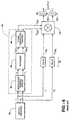
- filter 150 includes a taped delay line comprised of a plurality of delay line elements 152. Each tap is provided to a first input of respective multiplier 154. A second input of each multiplier 154 is provided with one of coefficients A as determined by equation (10) above. The outputs of all multipliers 154 are provided as inputs to summation circuit 156.
- Filter 150 is a transversal filter with a finite impulse response function. Such a filter is advantageously employed as filter 86 (FIG. 8).
- the present invention may be implemented in a current desk top computer under control of a program that mechanizes the functions described herein.
- the present invention maybe implemented in special hardware logic and arithmetic circuits.
- the present invention may be implemented in special applications specific integrated circuits (ASICs).
- ASICs applications specific integrated circuits
- the present invention may be implemented in customized gate array circuits.
- the present invention may be implemented in programmable digital signal processor integrated circuits.
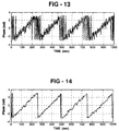
- FIGS. 14 depicts the averaged phase using a known Cartesian based averager (e.g., FIGS. 3-6).
- FIG. 15 depicts the averaged phase using the phase averager of equation (4), i.e, FIG. 8.
- FIG. 16 depicts the averaged phase using the phase averager of equation (2), i.e., FIG. 11.
- FIGS. 14-16 illustrate that the present invention achieves the same phase average performance as as known averagers without the need to provide a means for converting back and forth between Cartesian and polar coordinates.
Landscapes
- Engineering & Computer Science (AREA)
- Computer Networks & Wireless Communication (AREA)
- Signal Processing (AREA)
- Digital Transmission Methods That Use Modulated Carrier Waves (AREA)
- Synchronisation In Digital Transmission Systems (AREA)
Claims (15)
- Circuit de calcul de moyenne de phase (30) destiné à un estimateur de phase, le circuit de calcul de moyenne de phase comprenant :un circuit de différenciation de phase (82) couplé à l'entrée du circuit de calcul de moyenne de phase,un premier circuit modulo (84) couplé au circuit de différenciation de phase,un filtre (86) couplé au premier circuit modulo, etun circuit de sommation (88) comportant une entrée positive et une entrée négative, l'entrée positive étant couplée à l'entrée du circuit de calcul de moyenne de phase, l'entrée négative étant couplée au filtre (86).
- Circuit selon la revendication 1, comprenant en outre un second circuit modulo (89) couplé au circuit de sommation.
- Circuit selon la revendication 1, dans lequel le filtre (86) comprend :une ligne à retard comportant une pluralité de prises (152),une pluralité de multiplicateurs (154), chaque multiplicateur comportant des première et seconde entrées, la première entrée de chaque multiplicateur étant couplée à une prise correspondante, un coefficient de filtre prédéterminé étant appliqué à la seconde entrée de chaque multiplicateur, etun circuit de sommation de filtre (156) étant couplé à la sortie de chaque multiplicateur.
- Circuit selon la revendication 3, dans lequelle nombre des multiplicateurs est de N-1, etchaque multiplicateur (154) est identifié par un index k où k est supérieur à zéro et k est inférieur ou égal à N, comprenant un moyen conçu pour calculer une moyenne de phase uniformément pondérée, où chaque pondération, indiquée par kn, avec 1 ≤ n ≤ N, est donnée par kn = 1 / N
etle coefficient de filtre prédéterminé fourni au ke multiplicateur est Ak et est donné par :
- Procédé de calcul de moyenne de phase dans un estimateur de phase, le procédé comprenant les étapes consistant à :recevoir un signal avec une pluralité d'échantillons, chacun présentant une phase associée,former une mesure de différence de phase entre une mesure de phase actuelle d'un échantillon sélectionné et une mesure de phase adjacente d'un échantillon adjacent à l'échantillon sélectionné,transformer la mesure de différence de phase en une mesure de phase différenciée entre -π et π radians,filtrer la mesure de phase différenciée, etformer une phase de soustraction en soustrayant la mesure de phase différenciée de la mesure de phase actuelle.
- Procédé selon la revendication 5, comprenant en outre une étape consistant à transformer la phase de soustraction en une phase entre -π et π radians.
- Procédé selon la revendication 5, dans lequel l'étape de filtrage comprend les étapes consistant à :former une pluralité de mesures de phases adjacentes,multiplier séparément chaque mesure de phase adjacente par un coefficient de filtre prédéterminé correspondant, etsommer tous les résultats de multiplications.
- Procédé selon la revendication 7, dans lequel :le nombre de mesures de phases dont on doit calculer la moyenne est N,le nombre de mesures de phases adjacentes est N-1,chaque coefficient de filtre prédéterminé est identifié par un index k où k est supérieur à zéro et k est inférieur ou égal à N,une moyenne de phase uniformément pondérée est calculée où chaque pondération, indiquée par kn, avec 1 ≤ n ≤ N, est donnée par kn = 1 / N
etle ke coefficient de filtre prédéterminé est Ak et est donné par :
- Circuit de calcul de moyenne de phase pour un estimateur de phase, le circuit de calcul de moyenne de phase comprenant :une ligne à retard (112) comportant une pluralité de prises (114) couplée à une entrée de circuit de calcul de moyenne de phase,une pluralité de premiers circuits de soustraction (118), la première entrée de chaque premier circuit de soustraction étant couplée à l'entrée du circuit de calcul de moyenne de phase, la seconde entrée de chaque premier circuit de soustraction étant couplée à une prise correspondante de la pluralité de prises,une pluralité de premiers circuits modulo (122), chaque premier circuit modulo étant couplé à un premier circuit de soustraction correspondant,un circuit de sommation (124) couplé à tous les premiers circuits modulo,un circuit de mise à l'échelle (126) couplé au circuit de sommation, etun second circuit de soustraction (128), la première entrée du second circuit de soustraction étant couplée à l'entrée du circuit de calcul de moyenne de phase, la seconde entrée du second circuit de soustraction étant couplée au circuit de mise à l'échelle.
- Circuit selon la revendication 9, comprenant en outre un second circuit modulo (129) couplé au second circuit de soustraction.
- Circuit selon la revendication 9, dans lequel le circuit de mise à l'échelle (126) est conçu pour multiplier l'entrée devant être mise à l'échelle par l'inverse du nombre d'échantillons dont on doit calculer la moyenne.
- Circuit selon la revendication 9, dans lequel :une porteuse de modulation présente une période T, etla ligne à retard comprend au moins quatre prises représentant les phases échantillonnées durant la période T.
- Procédé de calcul de moyenne de phase dans un estimateur de phase, le procédé comprenant les étapes consistant à :recevoir un signal avec une pluralité d'échantillons, chacun présentant une phase associée,former une pluralité de mesures de phases adjacentes,former une pluralité de premières mesures de phases de soustraction en soustrayant chaque mesure de phase adjacente d'une mesure de phase actuelle, la phase actuelle étant sélectionnée à partir de la pluralité de phases adjacentes,former une pluralité de premières phases modulo en transformant chaque première mesure de phase de soustraction en une phase entre -π et π radians,former une mesure de phase de sommation en sommant toutes les premières phases modulo,mettre à l'échelle la mesure de phase de sommation, etformer une seconde mesure de phase de soustraction en soustrayant la mesure de phase mise à l'échelle de la mesure de phase actuelle.
- Procédé selon la revendication 13, comprenant en outre une étape supplémentaire consistant à transformer la seconde mesure de phase de soustraction en une phase entre -π et π radians.
- Procédé selon la revendication 13, dans lequel l'étape de mise à l'échelle multiplie une entrée devant être mise à l'échelle par l'inverse du nombre d'échantillons dont on doit calculer la moyenne.
Applications Claiming Priority (3)
| Application Number | Priority Date | Filing Date | Title |
|---|---|---|---|
| US749025 | 1985-06-26 | ||
| US08/749,025 US5960044A (en) | 1996-11-14 | 1996-11-14 | Apparatus and method for block phase estimation |
| PCT/US1997/020499 WO1998024202A2 (fr) | 1996-11-14 | 1997-11-10 | Appareil et procede d'estimation de phase dans des blocs |
Publications (3)
| Publication Number | Publication Date |
|---|---|
| EP1012966A2 EP1012966A2 (fr) | 2000-06-28 |
| EP1012966A4 EP1012966A4 (fr) | 2001-07-11 |
| EP1012966B1 true EP1012966B1 (fr) | 2004-05-26 |
Family
ID=25011917
Family Applications (1)
| Application Number | Title | Priority Date | Filing Date |
|---|---|---|---|
| EP97947437A Expired - Lifetime EP1012966B1 (fr) | 1996-11-14 | 1997-11-10 | Appareil et procede d'estimation de phase par blocs |
Country Status (5)
| Country | Link |
|---|---|
| US (1) | US5960044A (fr) |
| EP (1) | EP1012966B1 (fr) |
| JP (2) | JP3859174B2 (fr) |
| DE (1) | DE69729329T2 (fr) |
| WO (1) | WO1998024202A2 (fr) |
Families Citing this family (15)
| Publication number | Priority date | Publication date | Assignee | Title |
|---|---|---|---|---|
| US6633255B2 (en) * | 1995-10-09 | 2003-10-14 | Qualcomm Inc. | Method for open loop tracking GPS signals |
| US6134286A (en) * | 1997-10-14 | 2000-10-17 | Ericsson Inc. | Synchronization techniques and systems for radiocommunication |
| US6049297A (en) * | 1998-11-19 | 2000-04-11 | Visidyne, Corp. | Digital phase measuring system and method |
| US6567480B1 (en) * | 1999-08-10 | 2003-05-20 | Lucent Technologies Inc. | Method and apparatus for sampling timing adjustment and frequency offset compensation |
| US6724847B1 (en) * | 2000-09-06 | 2004-04-20 | Motorola, Inc. | Feed-forward symbol synchronizer and methods of operation therefor |
| US6879647B1 (en) | 2000-09-29 | 2005-04-12 | Northrop Grumman Corporation | Radio receiver AM-MSK processing techniques |
| US6993095B2 (en) * | 2001-03-15 | 2006-01-31 | Texas Instruments Incorporated | Phase-locked loop initialization via curve-fitting |
| EP1278346B1 (fr) * | 2001-07-19 | 2006-08-23 | TransCore Link Logistics Corporation | Dispositif de poursuite de phase pour signaux linéairment modulés |
| AU2003243516B2 (en) * | 2002-06-11 | 2009-03-19 | First Data Corporation | Value processing network and methods |
| US6707255B2 (en) * | 2002-07-10 | 2004-03-16 | Eni Technology, Inc. | Multirate processing for metrology of plasma RF source |
| US7336732B1 (en) * | 2004-07-28 | 2008-02-26 | L-3 Communications Titan Corporation | Carrier frequency detection for signal acquisition |
| KR100758873B1 (ko) * | 2005-12-30 | 2007-09-19 | 포스데이타 주식회사 | 무선통신 시스템의 주파수 오프셋 추정 장치 및 방법 |
| GB0609601D0 (en) * | 2006-05-15 | 2006-06-21 | Ttp Communications Ltd | Timing errors |
| US20110248757A1 (en) * | 2010-04-08 | 2011-10-13 | Saket Jalan | Digital calibration device and method for high speed digital systems |
| JP5380565B2 (ja) * | 2012-03-15 | 2014-01-08 | 株式会社東芝 | チャネル位相推定装置、復調器、受信機 |
Family Cites Families (14)
| Publication number | Priority date | Publication date | Assignee | Title |
|---|---|---|---|---|
| US3956623A (en) * | 1974-10-21 | 1976-05-11 | Gte Automatic Electric Laboratories Incorporated | Digital phase detector |
| EP0204745B2 (fr) * | 1984-11-22 | 1995-09-06 | Devon County Council | Systeme modem de donnees |
| DE3700457C1 (de) * | 1987-01-09 | 1988-06-23 | Ant Nachrichtentech | Verfahren und Anordnung zur Synchronisation eines Empfaengers bei digitalen UEbertragungssystemen |
| US4885757A (en) * | 1987-06-01 | 1989-12-05 | Texas Instruments Incorporated | Digital adaptive receiver employing maximum-likelihood sequence estimation with neural networks |
| US5001424A (en) * | 1989-02-03 | 1991-03-19 | Product Resources, Inc. | Apparatus for measuring magnetic particles suspended in a fluid based on fluctuations in an induced voltage |
| US5303269A (en) * | 1990-11-01 | 1994-04-12 | Chirp Corporation | Optically maximum A posteriori demodulator |
| US5283815A (en) * | 1991-05-21 | 1994-02-01 | General Electric Company | Tangental type differential detector for pulse shaped PI/4 shifted differentially encoded quadrature phase shift keying |
| US5202901A (en) * | 1991-05-21 | 1993-04-13 | General Electric Company | Digital discriminator for pulse shaped π/4 shifted differentially encoded quadrature phase shift keying |
| US5311545A (en) * | 1991-06-17 | 1994-05-10 | Hughes Aircraft Company | Modem for fading digital channels affected by multipath |
| US5375140A (en) * | 1992-11-24 | 1994-12-20 | Stanford Telecommunications, Inc. | Wireless direct sequence spread spectrum digital cellular telephone system |
| JP2797916B2 (ja) * | 1993-08-05 | 1998-09-17 | 日本電気株式会社 | 搬送波再生回路 |
| US5465271A (en) * | 1993-08-20 | 1995-11-07 | General Electric Company | Post detection weighted vector combining diversity receivers using phase metrics for mobile and indoor radio channels |
| US5497400A (en) * | 1993-12-06 | 1996-03-05 | Motorola, Inc. | Decision feedback demodulator with phase and frequency estimation |
| US5499273A (en) * | 1995-05-11 | 1996-03-12 | Motorola, Inc. | Method and apparatus for symbol clock recovery from signal having wide frequency possibilities |
-
1996
- 1996-11-14 US US08/749,025 patent/US5960044A/en not_active Expired - Lifetime
-
1997
- 1997-11-10 DE DE69729329T patent/DE69729329T2/de not_active Expired - Lifetime
- 1997-11-10 JP JP52467898A patent/JP3859174B2/ja not_active Expired - Fee Related
- 1997-11-10 EP EP97947437A patent/EP1012966B1/fr not_active Expired - Lifetime
- 1997-11-10 WO PCT/US1997/020499 patent/WO1998024202A2/fr not_active Ceased
-
2003
- 2003-10-31 JP JP2003373714A patent/JP2004088806A/ja not_active Withdrawn
Also Published As
| Publication number | Publication date |
|---|---|
| WO1998024202A3 (fr) | 1998-10-15 |
| JP2004088806A (ja) | 2004-03-18 |
| JP2001515668A (ja) | 2001-09-18 |
| US5960044A (en) | 1999-09-28 |
| DE69729329T2 (de) | 2005-08-25 |
| EP1012966A2 (fr) | 2000-06-28 |
| DE69729329D1 (de) | 2004-07-01 |
| WO1998024202A2 (fr) | 1998-06-04 |
| JP3859174B2 (ja) | 2006-12-20 |
| EP1012966A4 (fr) | 2001-07-11 |
Similar Documents
| Publication | Publication Date | Title |
|---|---|---|
| EP1012966B1 (fr) | Appareil et procede d'estimation de phase par blocs | |
| US4577334A (en) | Digital data receiver including timing adjustment circuit | |
| US4583048A (en) | MSK digital demodulator for burst communications | |
| US5566211A (en) | Automatic frequency control method and apparatus therefor | |
| EP0772330A2 (fr) | Récepteur et méthode de réception de signaux MDFO | |
| KR0157500B1 (ko) | 자동주파수조절방법 및 그 장치 | |
| US5805017A (en) | Baseband demodulation of M-ary frequency shift keyed signals and a receiver therefor | |
| US6415004B1 (en) | Phase detector, timing recovery device using the same, and a demodulator using the timing recovery device | |
| US6075408A (en) | OQPSK phase and timing detection | |
| CN111884964B (zh) | 适应vde多调制体制的频率同步系统 | |
| US5627861A (en) | Carrier phase estimation system using filter | |
| US5640427A (en) | Demodulator | |
| EP0763919B1 (fr) | Démodulateur "QPSK" avec poursuite de fréquence et de phase | |
| EP0486839B1 (fr) | Démodulateur MPSK quasi-cohérent | |
| US20070253512A1 (en) | Method for acquiring timing and carrier synchronization of offset-QPSK modulated signals | |
| US5640125A (en) | Digital PSK-type demodulator having clock recovery before carrier recovery | |
| US7778359B2 (en) | Method and device for clock synchronisation with a vestigial-sideband-modulated transmitted signal | |
| US7457375B2 (en) | Timing extractor, timing extraction method, and demodulator having the timing extractor | |
| KR100433639B1 (ko) | 잔류측파대변조시타이밍회복을위한장치및방법 | |
| US20250351105A1 (en) | Signal-Agnostic Apparatus, System, and Method for Doppler Correction | |
| JP2765601B2 (ja) | 復調回路 | |
| JP3185725B2 (ja) | 搬送波再生回路 | |
| KR0157498B1 (ko) | 자동주파수조절장치 | |
| JPH10303996A (ja) | 周波数ずれ検出方法と周波数ずれ検出装置 | |
| KR0157499B1 (ko) | 자동주파수조절방법 및 그 장치 |
Legal Events
| Date | Code | Title | Description |
|---|---|---|---|
| PUAI | Public reference made under article 153(3) epc to a published international application that has entered the european phase |
Free format text: ORIGINAL CODE: 0009012 |
|
| 17P | Request for examination filed |
Effective date: 19990602 |
|
| AK | Designated contracting states |
Kind code of ref document: A2 Designated state(s): DE FR GB IT NL |
|
| RAP1 | Party data changed (applicant data changed or rights of an application transferred) |
Owner name: SCIENTIFIC-ATLANTA, INC. |
|
| A4 | Supplementary search report drawn up and despatched |
Effective date: 20010530 |
|
| AK | Designated contracting states |
Kind code of ref document: A4 Designated state(s): DE FR GB IT NL |
|
| RIC1 | Information provided on ipc code assigned before grant |
Free format text: 7H 03D 3/00 A, 7H 04L 27/233 B |
|
| 17Q | First examination report despatched |
Effective date: 20020429 |
|
| GRAP | Despatch of communication of intention to grant a patent |
Free format text: ORIGINAL CODE: EPIDOSNIGR1 |
|
| GRAS | Grant fee paid |
Free format text: ORIGINAL CODE: EPIDOSNIGR3 |
|
| GRAA | (expected) grant |
Free format text: ORIGINAL CODE: 0009210 |
|
| AK | Designated contracting states |
Kind code of ref document: B1 Designated state(s): DE FR GB IT NL |
|
| PG25 | Lapsed in a contracting state [announced via postgrant information from national office to epo] |
Ref country code: NL Free format text: LAPSE BECAUSE OF FAILURE TO SUBMIT A TRANSLATION OF THE DESCRIPTION OR TO PAY THE FEE WITHIN THE PRESCRIBED TIME-LIMIT Effective date: 20040526 Ref country code: IT Free format text: LAPSE BECAUSE OF FAILURE TO SUBMIT A TRANSLATION OF THE DESCRIPTION OR TO PAY THE FEE WITHIN THE PRESCRIBED TIME-LIMIT;WARNING: LAPSES OF ITALIAN PATENTS WITH EFFECTIVE DATE BEFORE 2007 MAY HAVE OCCURRED AT ANY TIME BEFORE 2007. THE CORRECT EFFECTIVE DATE MAY BE DIFFERENT FROM THE ONE RECORDED. Effective date: 20040526 |
|
| REG | Reference to a national code |
Ref country code: GB Ref legal event code: FG4D |
|
| REF | Corresponds to: |
Ref document number: 69729329 Country of ref document: DE Date of ref document: 20040701 Kind code of ref document: P |
|
| NLV1 | Nl: lapsed or annulled due to failure to fulfill the requirements of art. 29p and 29m of the patents act | ||
| ET | Fr: translation filed | ||
| PLBE | No opposition filed within time limit |
Free format text: ORIGINAL CODE: 0009261 |
|
| STAA | Information on the status of an ep patent application or granted ep patent |
Free format text: STATUS: NO OPPOSITION FILED WITHIN TIME LIMIT |
|
| 26N | No opposition filed |
Effective date: 20050301 |
|
| REG | Reference to a national code |
Ref country code: FR Ref legal event code: PLFP Year of fee payment: 19 |
|
| REG | Reference to a national code |
Ref country code: FR Ref legal event code: PLFP Year of fee payment: 20 |
|
| PGFP | Annual fee paid to national office [announced via postgrant information from national office to epo] |
Ref country code: FR Payment date: 20161123 Year of fee payment: 20 Ref country code: GB Payment date: 20161128 Year of fee payment: 20 Ref country code: DE Payment date: 20161123 Year of fee payment: 20 |
|
| REG | Reference to a national code |
Ref country code: DE Ref legal event code: R071 Ref document number: 69729329 Country of ref document: DE |
|
| REG | Reference to a national code |
Ref country code: GB Ref legal event code: PE20 Expiry date: 20171109 |
|
| PG25 | Lapsed in a contracting state [announced via postgrant information from national office to epo] |
Ref country code: GB Free format text: LAPSE BECAUSE OF EXPIRATION OF PROTECTION Effective date: 20171109 |
|
| REG | Reference to a national code |
Ref country code: GB Ref legal event code: 732E Free format text: REGISTERED BETWEEN 20200312 AND 20200318 |
|
| REG | Reference to a national code |
Ref country code: DE Ref legal event code: R082 Ref document number: 69729329 Country of ref document: DE Representative=s name: BOSCH JEHLE PATENTANWALTSGESELLSCHAFT MBH, DE Ref country code: DE Ref legal event code: R081 Ref document number: 69729329 Country of ref document: DE Owner name: CISCO TECHNOLOGY, INC., SAN JOSE, US Free format text: FORMER OWNER: SCIENTIFIC-ATLANTA, INC., LAWRENCEVILLE, GA., US |
|
| REG | Reference to a national code |
Ref country code: DE Ref legal event code: R082 Ref document number: 69729329 Country of ref document: DE Representative=s name: BOSCH JEHLE PATENTANWALTSGESELLSCHAFT MBH, DE Ref country code: DE Ref legal event code: R081 Ref document number: 69729329 Country of ref document: DE Owner name: CISCO TECHNOLOGY, INC., SAN JOSE, US Free format text: FORMER OWNER: SCIENTIFIC-ATLANTA, LLC, LAWRENCEVILLE, GA, US |