EP1054475B1 - Appareil de contact et élément de contact associé - Google Patents
Appareil de contact et élément de contact associé Download PDFInfo
- Publication number
- EP1054475B1 EP1054475B1 EP20000110830 EP00110830A EP1054475B1 EP 1054475 B1 EP1054475 B1 EP 1054475B1 EP 20000110830 EP20000110830 EP 20000110830 EP 00110830 A EP00110830 A EP 00110830A EP 1054475 B1 EP1054475 B1 EP 1054475B1
- Authority
- EP
- European Patent Office
- Prior art keywords
- contact
- contact element
- holder
- section
- abutment
- Prior art date
- Legal status (The legal status is an assumption and is not a legal conclusion. Google has not performed a legal analysis and makes no representation as to the accuracy of the status listed.)
- Expired - Lifetime
Links
Images


Classifications
-
- H—ELECTRICITY
- H01—ELECTRIC ELEMENTS
- H01R—ELECTRICALLY-CONDUCTIVE CONNECTIONS; STRUCTURAL ASSOCIATIONS OF A PLURALITY OF MUTUALLY-INSULATED ELECTRICAL CONNECTING ELEMENTS; COUPLING DEVICES; CURRENT COLLECTORS
- H01R13/00—Details of coupling devices of the kinds covered by groups H01R12/70 or H01R24/00 - H01R33/00
- H01R13/02—Contact members
- H01R13/22—Contacts for co-operating by abutting
- H01R13/24—Contacts for co-operating by abutting resilient; resiliently-mounted
- H01R13/2442—Contacts for co-operating by abutting resilient; resiliently-mounted with a single cantilevered beam
-
- H—ELECTRICITY
- H01—ELECTRIC ELEMENTS
- H01R—ELECTRICALLY-CONDUCTIVE CONNECTIONS; STRUCTURAL ASSOCIATIONS OF A PLURALITY OF MUTUALLY-INSULATED ELECTRICAL CONNECTING ELEMENTS; COUPLING DEVICES; CURRENT COLLECTORS
- H01R12/00—Structural associations of a plurality of mutually-insulated electrical connecting elements, specially adapted for printed circuits, e.g. printed circuit boards [PCB], flat or ribbon cables, or like generally planar structures, e.g. terminal strips, terminal blocks; Coupling devices specially adapted for printed circuits, flat or ribbon cables, or like generally planar structures; Terminals specially adapted for contact with, or insertion into, printed circuits, flat or ribbon cables, or like generally planar structures
- H01R12/70—Coupling devices
- H01R12/71—Coupling devices for rigid printing circuits or like structures
- H01R12/712—Coupling devices for rigid printing circuits or like structures co-operating with the surface of the printed circuit or with a coupling device exclusively provided on the surface of the printed circuit
- H01R12/716—Coupling device provided on the PCB
Definitions
- the present invention relates to a contacting apparatus, which will be referred to below as a contact block.
- the contact block serves in particular for contacting contacting zones of a so-called smart card.
- the invention relates in particular to a so-called SIM block (trademark), i. e. a contacting apparatus which is suitable for providing an electrical contact connection to contact zones present on a SIM card.
- SIM block trademark
- WO-A-9740467 discloses a contact block with a holder.
- the holder comprises a plurality of contact elements adapted to provide an electrical connection between a circuit board and a surface contact of a SIM modul.
- the contact elements are provided with spring cusps adapted to provide a connection with surface contacts of the circuit board.
- FR-A-2763412 discloses a SIM card connector with contact elements mounted in a holder so as to contact the contact zones of a SIM card inserted into a cover at the time the cover is closed.
- the present invention intends, in particular, to provide a SIM block which has a very small height, for instance in the range of 0.8 mm.
- a small height for the SIM block is obtained by providing contact elements for the SIM block, such that as the contact force exerted by the contact zones of a SIM card onto the contact elements is transmitted by support means formed by or provided at the contact elements to another component, in particular, a circuit board which is adapted to support said SIM block.
- the invention further provides for adjustment means, which are preferably provided together with the support means to thus provide for the possibility of adjusting the force, by means of which the contact elements press against the contact zones of the SIM card.
- a contact block as set forth in claim 1 and a contact element as set forth in claim 19 are provided.
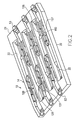
- a contacting apparatus 10 in the form of a SIM block 10, which is mounted on a printed circuit board 11.
- the SIM block 10 comprises contact elements 13 and a contact support or holder 14, within which the contact elements 13 are mounted.
- the circuit board 11 comprises soldering surfaces 12 with which the contact element 13 can be physically and electrically connected by soldering a soldering zone of the contact element 13 to the soldering surface 12.
- the soldering zone is formed by a termination end 53 of the contact element 13, as will be described below.
- circuit board 11 could be provided with contact surfaces instead of soldering surfaces 12. At said contact surfaces of the circuit board 11 pressure contact zones of the pressure contact elements could resiliently abut.
- the holder 14 is, see Fig. 1 , preferably made of plastic material and comprises an upper surface 20 and a lower or bottom surface 21. Slotlike openings (short slots) 22 extend through the thickness of the wall forming the upper surface 20 of the holder 14. Said slots 22 allow bulged contact ends 54 of the contact elements 13 to extend therethrough to a level above the upper surface 20. In the shown embodiment six contact elements 13 are used. The contact elements 13 are mounted in said holder 14 in an interleaving manner, with the termination ends 53 located in opposite directions in an alternate manner. The termination ends 53 of the six contact elements 13 are soldered alternately to soldering surfaces 12.
- Slots 23 are provided in the holder 14, in the area where the bulged contact ends 54 project beyond the upper surface 20.
- the slots 23 define ribs 24 in the holder 14 and provide a certain amount of resiliency, so that they can be deflected transversally with respect to the longitudinal direction L ( Fig. 1 ) of the SIM block 18, when the contact elements 13 are inserted into the holder 14.
- Said slots 23 are located in the vicinity of projections 126, 127 ( Fig. 2 and 4 ) yet to be described.
- the slots 22 are at least partially open at each of the two small sides of the holder 14, in an alternate manner.
- Detent recesses 26, 27, see Fig. 4 are provided in holder 14 and are adapted to receive each one contact element 13. Inclined portions 28, 29 allow easy insertion of the contact element 13 into the recesses 26, 27.
- the recesses 26, 27 are located in the area of the slots 23.
- the recesses 26, 27 are formed in respective oppositely located projections 126, 127 of the holder 14. The projections 126, 127 project, see Fig. 4 , into the slots 22.
- the holder 14 forms - see Fig. 7 - at the closed end of each slot 22 an abutment incline 30. If no force F is applied by a SIM card pressing against the contact elements 13 (see Fig. 7 ), abutment portions 55 of the contact elements 13 are in biased abutment with the abutment inclines 30.
- Fig. 3 shows the contact element 13 in form of a contact spring, which has in substance an elongate form and comprises the following sections; a contact section 40 for contacting a contact zone of a SIM card, a connecting and spring section 41, an abutment section 42 and a termination section 43.
- the termination section 43 the termination end 53, already mentioned, is formed.
- connection and spring section 41 an opening 46 is formed, which is for example used for connection with the holder 14.
- support means 87 are provided adjacent to the abutment section 42.
- the support means 87 are integrally formed as a single piece with the contact element 13.
- the support means 87 comprise at both sides, rib means 47, 48. Said rib means 47, 48 form at their ends facing towards the contact section 40, arms 50, 51.
- the arms 50, 51 (also called adjustment springs 50, 51) transfer the force to the circuit board 11.
- the two adjustment springs 50, 51 provide for adjustment of the force by changing the inclination of the adjustment springs 50, 51 with respect to the longitudinal axis L of the contact block. Alternatively, the length of the adjustment springs 50, 51 could be changed.
- the rib means 47 comprise two ribs 71 and 72, separated by a recess 70.
- the rib means 48 comprise two ribs 81 and 82, separated by a recess 80.
- the detent mounting of the contact elements 13 in the holder 14 occurs preferably, as will be explained below in detail, in the area of the recesses 70 and 80.
- the rib means 47, 48 comprise preferably abutment surfaces 56, 57, 58, 59 arranged on the same level, forming an abutment plane 257 ( Fig. 2 ) described below.
- the abutment surfaces 56-59 are adapted to be placed on the circuit board 11.
- Each of said contact elements 13 comprises in the termination section 43 said termination end 53 and in the contact section 40 the already mentioned bulged contact end 54. Adjacent to the contact end 54 an abutment portion 55 is formed.
- the termination ends 53 are biased, so that all the termination ends 53 are located in the same plane, i. e. are coplanar.
- Fig. 2 as well as Fig. 4 and 5 show in particular the detent mounting of the contact elements 13 in the support 14.
- the support 14 forms in the area of the slots 22 projections 126 and 127.
- the projections 126 and 127 are arranged on both sides of the slots 22 and extend into the interior of said slots.
- the recesses 26 and 27 formed in the projections 126 and 127 are adapted to receive the contact elements in the area of the recesses 70 and 80.
- Fig. 4 discloses that the support 14 forms a post 100 which projects through the opening 46 of the contact element 13, when the contact element 13 is in its mounted position in the support 14.
- the post or projection 100 serves for guiding and mounting said contact element 13. It is possible that the upper end of the post 100 is coined (pressed) onto the contact element 13 so as to fixedly mount said contact element 13 at the support 14. In such a case it is conceivable that the contact element 13 does not need to be mounted in the support 14 by detent means. More than one post 100 and more than one opening 46 can be provided.
- Fig. 4 discloses further that the height BH of the contact block 10 is small, for instance in the area of 0.8 mm. For all practical purposes, the height BH of the contact block 10 is determined by the height of the contact element 13.
- Both Fig. 2 and also Fig. 4 show clearly that the contact elements 13 can be inserted in accordance with the invention from the bottom side 21 of the holder 14 (see also Fig. 1 ) into said holder 14.
- Fig. 6 discloses that the contact element 13, when fixedly mounted in the holder 14, is biased against said holder 14 in its termination area 43.
- the termination end 53 of the termination section 43 is, prior to the insertion of the contact element 13 into the holder 14, in the position shown by a dotted line. After the insertion of the contact element 13 into the holder 14 the termination end 53 assumes the position shown with solid lines, and is biased against the contact element 13. In this manner, coplanarity is readily achieved.
- Fig. 7 discloses in detail the fact that the contact element 13 is biased with its contact section 40 against the holder 14.
- the abutment portion 55 of the bulged contact end 54 is in abutment with an abutment incline 30 of the holder 14.
- Fig. 7 also discloses schematically the path of the force via the two adjustment springs 50, 51 onto the circuit board 11.
- Fig. 2 shows that six contact elements 13 are inserted into the holder 14 and are fixedly mounted therein due to the fact that the areas of the contact elements 13 comprising the recesses 70, 80 have been pressed through the gaps formed by the projections 126 and 127.
- the contact element 13 is guided by the inclined portions 28 and 29 of the projections 126 and 127, resiliently bending the projections 126 and 127 away from each other.
- the projections 126 and 127 move back into the positions shown in Fig. 4 and thus fixedly hold the contact element 13 in the holder 14.
- the projections 126, 127, the recesses 26, 27 and the contact elements 13 form together detent means.
- Fig. 2 discloses that the six contact elements 13 inserted into the holder 14 define with the upwardly facing surfaces ( Fig. 2 ) of the six termination ends 53 a soldering plane 253, shown schematically in Fig. 2 . It should be noted that in Fig. 2 the contact elements 13 are soldering contact elements, and, as such, are shown with soldering termination ends 53.
- abutment surfaces 56 to 59 define an abutment plane 257 as is shown schematically in Fig. 2 .
- Fig. 8 discloses another embodiment of a contact element 130, which corresponds in some respects to contact element 13.
- Contact element 130 comprises like the contact element 13 a contact section 40 and a termination section 143.
- contact element 130 comprises an opening 46 for cooperation with a post 100 of the holder 14.
- the support means 87 is not formed by rib means, but the support means 87 is formed by a bulged or bight section 187 of contact element 130.
- a bottom surface 188 of the bulged portion or section 187 can be in abutment with the surface of a circuit board 11 so as to transmit the contact force directly onto the circuit board 11.
- Fig. 9 discloses for the contact element 130 that in accordance with the invention a small gap or a height difference H can be provided between a soldering plane and an abutment plane similar to what was described in relation with Fig. 2 for contact element 13.
- the bottom surfaces 188 of the contact elements 130 form an abutment plane similar to the abutment plane 257 explained above.
- the termination means i. e. the connection between the termination ends 53 with the soldering surfaces 12 of the printed circuit board 11 extend outwardly from the support 13.
- the soldering points of the soldering contact elements can be checked after the soldering operation has been carried out.
- termination ends 53 could also be formed as pressure termination ends and not, as shown, as SMT termination ends.
- the invention provides for a safe and secure support of the contact elements on a circuit board 11 or any other component.
- the invention further provides for a small height of the contact block 10. Moreover it is readily possible to adjust the force of the contact element without requiring additional components.
- the small height of the contact block 10 is particularly due to the fact that the contact elements 13, 130 are supported directly on the printed circuit board 11. There is no need to provide for an insulating layer of the holder 13 between the contact elements 13, 130 and the upper surface of the printed circuit board 11.
- the contact elements 13 and 130 can be adjusted and optimized by changing the geometry of the contact element. Further, instead of using slots 23 in the contact support 14, it is also possible to provide slots in the contact element 13, 130 in the area where the detent mounting is provided.
- the contact elements could be mounted in a different manner at the holder contact support 14.
- the contact elements could be provided with claws, which penetrate into the insulating material, out of which the holder 14 is formed, so as to fixedly mount said contact elements in the holder 14.
- the contact elements 13, 130 could also be fixedly mounted in said holder 14 by, as mentioned above, coining operations.
Landscapes
- Coupling Device And Connection With Printed Circuit (AREA)
Claims (32)
- Bloc de contact, en particulier bloc SIM comportant un support (14) dans lequel sont insérés des éléments de contact (13) ; dans lequel chacun des éléments de contact (13) comprend un moyen de support (87, 187) pour porter l'élément de contact (13) et pour buter contre un autre composant, par exemple une carte de circuit imprimé (11), le moyen de support (87, 187) étant formé d'une seule pièce de façon solidaire avec les éléments de contact (13, 130) et dans lequel les éléments de contact (13) sont des ressorts de contact qui s'étendent essentiellement dans la direction longitudinale et comprennent à une extrémité une partie de terminaison (43, 143) et à une extrémité opposée une partie de contact (40) ayant une extrémité de contact bombée (54), le moyen de support (87) pour buter contre un autre composant étant prévu entre la partie de terminaison (43, 143) et la partie de contact (40).
- Bloc de contact selon la revendication 1, dans lequel le moyen de support (87) est en forme de moyen de nervure (47, 48) adaptés à buter contre la carte de circuit imprimé (11).
- Bloc de contact selon l'une quelconque des revendications précédentes, dans lequel le moyen de nervure comprend des nervures disposées de façon opposée (71, 72, 81, 82) chacune des nervures (47, 48) étant séparée par un évidement (70, 80).
- Bloc de contact selon la revendication 1 ou 2, dans lequel le moyen de support (87) est constitué d'une partie bombée (187) de l'élément de contact (130).
- Bloc de contact selon l'une quelconque des revendications 1 à 4, dans lequel les éléments de contact (13) sont montés fixes dans le support (14) par un moyen de ressort.
- Bloc de contact selon l'une quelconque des revendications précédentes, dans lequel les éléments de contact (13, 130) sont montés fixes dans le support (14) au moyen d'un ou plusieurs plots (100) formés par le support (14), les plots (100) faisant saillie à travers des ouvertures respectives (46) dans l'élément de contact (13).
- Bloc de contact selon l'une quelconque des revendications 2 et 4 à 6, dans lequel le moyen de nervure (47, 48) comprend des bras (50, 51) qui peuvent être modifiés en ce qui concerne leur position angulaire et/ou leur longueur.
- Bloc de contact selon la revendication 7, dans lequel les bras (50, 51) sont disposés dans une partie de connexion et de ressort (41) de l'élément de contact (13) tournée vers une partie de contact (40) de l'élément de contact (13).
- Bloc de contact selon la revendication 7 ou 8, dans lequel des fentes (22) sont prévues dans le support (14) et adaptées à recevoir les éléments de contact (13, 130).
- Bloc de contact selon l'une quelconque des revendications précédentes, dans lequel des évidements (26, 27) sont formés dans le support (14), les évidements étant adaptés à recevoir des parties de l'élément de contact (13), les parties étant maintenues dans le support (14) en raison d'une action de ressort.
- Bloc de contact selon la revendication 10, dans lequel l'élément de contact (13) est muni d'évidements (70, 80) qui sont adaptés à être insérés dans les évidements (26, 27) du support (14) par une action de ressort.
- Bloc de contact selon la revendication 10 ou 11, dans lequel le plot (100) fait saillie dans une ouverture (46) de l'élément de contact (13) et a une forme ovale.
- Bloc de contact selon l'une quelconque des revendications précédentes, dans lequel le support (14) comprend des fentes (23) dans la zone où l'action de ressort prend place.
- Bloc de contact selon la revendication 13, dans lequel les évidements (26, 27) sont formés dans des saillies (126, 127) formés par le support (14).
- Bloc de contact selon l'une quelconque des revendications précédentes, dans lequel l'élément de contact (13) monté dans le support (14) est sollicité contre le support (14) par une section de terminaison (43) de l'élément de contact.
- Bloc de contact selon l'une quelconque des revendications 1 à 14, dans lequel l'élément de contact (13) est sollicité contre le support (14) avec une partie de butée (55) dans une partie de contact (40) de l'élément de contact (13), et dans lequel les éléments de contact (13) insérés dans le support (14) définissent :a) par des extrémités de terminaison, un plan de soudure (253) ;b) par des surfaces de butée (56-59), un plan de butée (247), une différence de hauteur (H) étant prévue entre le plan de soudure (253) et le plan de butée (247).
- Bloc de contact selon l'une quelconque des revendications 1 à 16, dans lequel les éléments de contact (13) peuvent être insérés dans le support (14) à partir de la surface inférieure (21).
- Bloc de contact selon l'une quelconque des revendications précédentes, dans lequel les éléments de contact (13) sont des éléments de contact de soudage ou des éléments de contact à pression.
- Elément de contact, en particulier pour bloc de contact dans lequel l'élément de contact (13) est un ressort de contact et s'étend sensiblement dans la direction longitudinale et comprend à une extrémité une partie de terminaison et à l'extrémité opposée une partie de contact, avec une partie de butée entre elles, la partie de butée constituant un moyen de support pour porter l'élément de contact et pour buter avec un autre composant, par exemple une carte de circuit imprimé, la partie de contact formant une extrémité de contact bombée (54), et dans lequel le moyen de support (87, 187) est formé d'une seule pièce solidaire des éléments de contact (13, 130).
- Elément de contact selon la revendication 19, dans lequel le moyen de support (87) est en forme de moyen de nervure (47, 48) adaptée à buter contre un autre composant tel qu'une carte de circuit imprimé (11).
- Elément de contact selon la revendication 20, dans lequel le moyen de nervure comprend des nervures disposées de façon opposée (71, 72, 81, 82) chacune des nervures (47, 48) étant séparée par un évidement (70, 80).
- Elément de contact selon l'une quelconque des revendications 19 à 21, dans lequel le moyen de support (87) est constitué d'une partie bombée (187) de l'élément de contact (130).
- Elément de contact selon l'une quelconque des revendications 19 à 22, dans lequel l'élément de contact (13) est adapté à être monté fixe dans le support (14) par un moyen de ressort.
- Elément de contact selon la revendication 23, dans lequel l'élément de contact (13, 130) est adapté à être monté fixe dans le support (14) au moyen d'un ou plusieurs plots (100) formés par le support (14), les plots (100) faisant saillie à travers des ouvertures respectives (46) dans l'élément de contact (13).
- Elément de contact selon la revendication 20 à 24, dans lequel le moyen de nervure (47, 48) comprend des bras (50, 51) qui peuvent être modifiés en ce qui concerne leurs positions angulaires et/ou leurs longueurs.
- Elément de contact selon la revendication 25, dans lequel les bras (50, 51) sont disposés dans une partie de connexion et de ressort (41) de l'élément de contact (13) tournée vers une partie de contact (40) de l'élément de contact (13).
- Elément de contact selon l'une quelconque des revendications 23 à 26, adapté à être reçu dans des fentes (22) prévues dans le support (14).
- Elément de contact selon l'une quelconque des revendications 23 à 27, adapté à être reçu avec des parties de l'élément de contact (13) dans des évidements (26, 27) formés dans le support (14), les parties étant maintenues dans le support (14) en raison d'une action de ressort.
- Elément de contact selon la revendication 28, dans lequel l'élément de contact (13) est muni d'évidements (70, 80) qui sont adaptés à être insérés dans les évidements (26, 27) du support (14) par une action de ressort.
- Elément de contact selon l'une quelconque des revendications 23 à 29, dans lequel l'élément de contact (13) monté dans le support (14) est sollicité contre le support (14) par une section de terminaison (43) de l'élément de contact.
- Elément de contact selon l'une quelconque des revendications 23 à 30, dans lequel les éléments de contact (13) peuvent être insérés dans le support (14) à partir de la surface inférieure (21).
- Elément de contact selon l'une quelconque des revendications 19 à 31, dans lequel les éléments de contact (13) sont des éléments de contact de soudage ou des éléments de contact à pression.
Applications Claiming Priority (4)
| Application Number | Priority Date | Filing Date | Title |
|---|---|---|---|
| DE19923405 | 1999-05-21 | ||
| DE19923405 | 1999-05-21 | ||
| DE10024711 | 2000-05-18 | ||
| DE10024711A DE10024711A1 (de) | 1999-05-21 | 2000-05-18 | Kontaktiereinrichtung sowie Kontaktelement dafür |
Publications (3)
| Publication Number | Publication Date |
|---|---|
| EP1054475A2 EP1054475A2 (fr) | 2000-11-22 |
| EP1054475A3 EP1054475A3 (fr) | 2005-08-10 |
| EP1054475B1 true EP1054475B1 (fr) | 2008-07-16 |
Family
ID=26005743
Family Applications (1)
| Application Number | Title | Priority Date | Filing Date |
|---|---|---|---|
| EP20000110830 Expired - Lifetime EP1054475B1 (fr) | 1999-05-21 | 2000-05-22 | Appareil de contact et élément de contact associé |
Country Status (1)
| Country | Link |
|---|---|
| EP (1) | EP1054475B1 (fr) |
Families Citing this family (1)
| Publication number | Priority date | Publication date | Assignee | Title |
|---|---|---|---|---|
| DE20101938U1 (de) | 2001-02-05 | 2001-06-07 | Tyco Electronics Nederland B.V., Hertogenbosch | Federndes Kontaktelement und Anordnung zur federnden Kontaktierung |
Family Cites Families (2)
| Publication number | Priority date | Publication date | Assignee | Title |
|---|---|---|---|---|
| JP2000508800A (ja) * | 1996-04-19 | 2000-07-11 | シーメンス アクチエンゲゼルシヤフト | カード読み取り装置 |
| FR2763412B1 (fr) * | 1997-05-13 | 1999-06-18 | Itt Mfg Enterprises Inc | Connecteur electrique pour une carte a circuit(s) integre(s) a contact |
-
2000
- 2000-05-22 EP EP20000110830 patent/EP1054475B1/fr not_active Expired - Lifetime
Also Published As
| Publication number | Publication date |
|---|---|
| EP1054475A2 (fr) | 2000-11-22 |
| EP1054475A3 (fr) | 2005-08-10 |
Similar Documents
| Publication | Publication Date | Title |
|---|---|---|
| KR100267161B1 (ko) | 전기통신케이블용 콘넥터구조 | |
| US6994566B2 (en) | Circuit board mounted electrical connector | |
| US5366380A (en) | Spring biased tapered contact elements for electrical connectors and integrated circuit packages | |
| EP0898792B1 (fr) | Pince laterale pour carte miniature | |
| JP3746106B2 (ja) | 基板用電気コネクタ | |
| US5411408A (en) | Electrical connector for printed circuit boards | |
| US6398598B2 (en) | Electrical connector | |
| US6120328A (en) | Thin smart card connector | |
| US6305960B1 (en) | SIM card connector with improved detecting switch | |
| US6261113B1 (en) | Electrical connector having improved arrangement of terminals | |
| US6368156B1 (en) | Audio jack conveniently and reliably mounted on a circuit board | |
| US5645445A (en) | Wire termination block | |
| KR100344050B1 (ko) | Pga 패키지용의 낮은 형상 전기 커넥터 및 단자 | |
| KR20020000004U (ko) | 표면 장착 전기 커넥터 | |
| US6530787B2 (en) | Coaxial plug connector for mounting on a circuit board | |
| KR100431468B1 (ko) | 인쇄회로기판에 칩 카드를 전기적으로 접속하기 위한 장치 | |
| KR19980702909A (ko) | 전기 리셉터클 어셈블리 및 그를 위한 스프링컨택트 | |
| US6126486A (en) | Smart card connector having contact retention means | |
| US6354891B1 (en) | Contacting apparatus and contact element therefore | |
| US6305948B1 (en) | Contact for surface mounted connector | |
| US6666711B2 (en) | Electrical connector for a circuit board | |
| NZ202553A (en) | Socket interfacing chip carrier with p.c.b. | |
| WO1995035550A1 (fr) | Connecteur pour cartes sim | |
| EP1054475B1 (fr) | Appareil de contact et élément de contact associé | |
| US6471535B1 (en) | Electrical socket |
Legal Events
| Date | Code | Title | Description |
|---|---|---|---|
| PUAI | Public reference made under article 153(3) epc to a published international application that has entered the european phase |
Free format text: ORIGINAL CODE: 0009012 |
|
| AK | Designated contracting states |
Kind code of ref document: A2 Designated state(s): AT BE CH CY DE DK ES FI FR GB GR IE IT LI LU MC NL PT SE |
|
| AX | Request for extension of the european patent |
Free format text: AL;LT;LV;MK;RO;SI |
|
| RIN1 | Information on inventor provided before grant (corrected) |
Inventor name: SCHNELL, THOMAS Inventor name: BRAUN, GERHARD Inventor name: LAAGE, ANDREAS |
|
| PUAL | Search report despatched |
Free format text: ORIGINAL CODE: 0009013 |
|
| AK | Designated contracting states |
Kind code of ref document: A3 Designated state(s): AT BE CH CY DE DK ES FI FR GB GR IE IT LI LU MC NL PT SE |
|
| AX | Request for extension of the european patent |
Extension state: AL LT LV MK RO SI |
|
| RIC1 | Information provided on ipc code assigned before grant |
Ipc: 7H 01R 13/24 A |
|
| 17P | Request for examination filed |
Effective date: 20060119 |
|
| AKX | Designation fees paid |
Designated state(s): DE FR |
|
| 17Q | First examination report despatched |
Effective date: 20060222 |
|
| GRAP | Despatch of communication of intention to grant a patent |
Free format text: ORIGINAL CODE: EPIDOSNIGR1 |
|
| GRAS | Grant fee paid |
Free format text: ORIGINAL CODE: EPIDOSNIGR3 |
|
| GRAA | (expected) grant |
Free format text: ORIGINAL CODE: 0009210 |
|
| AK | Designated contracting states |
Kind code of ref document: B1 Designated state(s): DE FR |
|
| REF | Corresponds to: |
Ref document number: 60039471 Country of ref document: DE Date of ref document: 20080828 Kind code of ref document: P |
|
| PLBE | No opposition filed within time limit |
Free format text: ORIGINAL CODE: 0009261 |
|
| STAA | Information on the status of an ep patent application or granted ep patent |
Free format text: STATUS: NO OPPOSITION FILED WITHIN TIME LIMIT |
|
| 26N | No opposition filed |
Effective date: 20090417 |
|
| PGFP | Annual fee paid to national office [announced via postgrant information from national office to epo] |
Ref country code: DE Payment date: 20100531 Year of fee payment: 11 |
|
| REG | Reference to a national code |
Ref country code: FR Ref legal event code: ST Effective date: 20110131 |
|
| PG25 | Lapsed in a contracting state [announced via postgrant information from national office to epo] |
Ref country code: FR Free format text: LAPSE BECAUSE OF NON-PAYMENT OF DUE FEES Effective date: 20100531 |
|
| REG | Reference to a national code |
Ref country code: DE Ref legal event code: R119 Ref document number: 60039471 Country of ref document: DE |
|
| REG | Reference to a national code |
Ref country code: DE Ref legal event code: R119 Ref document number: 60039471 Country of ref document: DE |
|
| PG25 | Lapsed in a contracting state [announced via postgrant information from national office to epo] |
Ref country code: DE Free format text: LAPSE BECAUSE OF NON-PAYMENT OF DUE FEES Effective date: 20111130 |
|
| PGFP | Annual fee paid to national office [announced via postgrant information from national office to epo] |
Ref country code: FR Payment date: 20090622 Year of fee payment: 10 |