EP1067763B1 - Système et procédé pour obtenir des images à haute facilité d'adressage - Google Patents
Système et procédé pour obtenir des images à haute facilité d'adressage Download PDFInfo
- Publication number
- EP1067763B1 EP1067763B1 EP00113728A EP00113728A EP1067763B1 EP 1067763 B1 EP1067763 B1 EP 1067763B1 EP 00113728 A EP00113728 A EP 00113728A EP 00113728 A EP00113728 A EP 00113728A EP 1067763 B1 EP1067763 B1 EP 1067763B1
- Authority
- EP
- European Patent Office
- Prior art keywords
- pixel
- value
- image data
- image
- high addressability
- Prior art date
- Legal status (The legal status is an assumption and is not a legal conclusion. Google has not performed a legal analysis and makes no representation as to the accuracy of the status listed.)
- Expired - Lifetime
Links
Images


Classifications
-
- G—PHYSICS
- G06—COMPUTING OR CALCULATING; COUNTING
- G06K—GRAPHICAL DATA READING; PRESENTATION OF DATA; RECORD CARRIERS; HANDLING RECORD CARRIERS
- G06K15/00—Arrangements for producing a permanent visual presentation of the output data, e.g. computer output printers
- G06K15/02—Arrangements for producing a permanent visual presentation of the output data, e.g. computer output printers using printers
- G06K15/10—Arrangements for producing a permanent visual presentation of the output data, e.g. computer output printers using printers by matrix printers
- G06K15/102—Arrangements for producing a permanent visual presentation of the output data, e.g. computer output printers using printers by matrix printers using ink jet print heads
-
- G—PHYSICS
- G06—COMPUTING OR CALCULATING; COUNTING
- G06K—GRAPHICAL DATA READING; PRESENTATION OF DATA; RECORD CARRIERS; HANDLING RECORD CARRIERS
- G06K15/00—Arrangements for producing a permanent visual presentation of the output data, e.g. computer output printers
- G06K15/02—Arrangements for producing a permanent visual presentation of the output data, e.g. computer output printers using printers
-
- H—ELECTRICITY
- H04—ELECTRIC COMMUNICATION TECHNIQUE
- H04N—PICTORIAL COMMUNICATION, e.g. TELEVISION
- H04N1/00—Scanning, transmission or reproduction of documents or the like, e.g. facsimile transmission; Details thereof
- H04N1/40—Picture signal circuits
- H04N1/405—Halftoning, i.e. converting the picture signal of a continuous-tone original into a corresponding signal showing only two levels
- H04N1/4051—Halftoning, i.e. converting the picture signal of a continuous-tone original into a corresponding signal showing only two levels producing a dispersed dots halftone pattern, the dots having substantially the same size
- H04N1/4052—Halftoning, i.e. converting the picture signal of a continuous-tone original into a corresponding signal showing only two levels producing a dispersed dots halftone pattern, the dots having substantially the same size by error diffusion, i.e. transferring the binarising error to neighbouring dot decisions
-
- G—PHYSICS
- G06—COMPUTING OR CALCULATING; COUNTING
- G06K—GRAPHICAL DATA READING; PRESENTATION OF DATA; RECORD CARRIERS; HANDLING RECORD CARRIERS
- G06K2215/00—Arrangements for producing a permanent visual presentation of the output data
- G06K2215/0002—Handling the output data
- G06K2215/0062—Handling the output data combining generic and host data, e.g. filling a raster
- G06K2215/0071—Post-treatment of the composed image, e.g. compression, rotation
-
- G—PHYSICS
- G06—COMPUTING OR CALCULATING; COUNTING
- G06K—GRAPHICAL DATA READING; PRESENTATION OF DATA; RECORD CARRIERS; HANDLING RECORD CARRIERS
- G06K2215/00—Arrangements for producing a permanent visual presentation of the output data
- G06K2215/0002—Handling the output data
- G06K2215/0077—Raster outputting to the print element(s)
Definitions
- This invention relates to systems and methods for generating high addressability images.
- the pixels in a binary image may be either on or off, i.e., black or white, respectively.
- the binary image may be a binary image possessing both highlights and shadows and having normal addressability.
- various devices have the capability to generate a high addressability image.
- a high addressability binary image is an image created by a device such that the spatial addressability of the image pixel by the device is finer than the size of the writing spot of that device.
- High addressability also often refers to an addressability resolution in a first direction that is finer than the spatial addressability resolution in a second direction that is, for example, perpendicular to the first direction.
- High addressability data can be used to render edges in text and line art regions at a high spatial precision in the high addressability direction.
- High addressability data can also be used in halftone regions to provide additional spatial resolution in the high addressability direction.
- Fig. 1 is a diagram showing a high addressability pixel grid.
- the spatial addressability of the pixels in the horizontal direction i.e., the fast scan direction
- the vertical direction i.e., the slow scan or process direction.
- Fig. 1 illustrates an image having a high addressability of 4. That is, each nominal "pixel" 114 contains four "subpixels" 124. This distinction between a pixel 114 and a subpixel 124 is used throughout this application. Images may have various other high addressability values, such as an addressability of 8.
- a high addressability image may be referred to as an "anamorphic" image since the high addressability image possesses different spatial resolutions in mutually perpendicular directions. In contrast, an "isomorphic" image possesses the same spatial resolution in mutually perpendicular directions.
- problems occur in conventional methods when inputting and manipulating images, and subsequently reproducing or printing high addressability images.
- problems occur in the conventional methods when printing high addressability binary images or image regions, such as images possessing shadows and highlights, for example.
- the image may be black and white only, or in color.
- Random access ink jet printers such as those disclosed in U.S. Patent 5,675,365 to Becerra et al., allow great flexibility in the sequence in which individual pixels are printed or fired. This occurs by allowing the individual ink ejections to be scheduled, rather than addressing them in a fixed order at a fixed clock speed. This scheduling allows more flexibility in which particular pixels may be printed to achieve a desired image on a recording medium using a choice of pixel firing patterns.
- an individual ink ejector is addressed at some frequency f. That ink ejector is either fired or not fired each time it is addressed.
- f a frequency that is much faster than f, i.e., at the clock rate.
- US 5,619,242 describes image forming apparatus with edge point detector based on image density charge.
- An image forming apparatus for forming an image on an image forming body by scanning a plurality of modulated laser beams is disclosed.
- the apparatus is provided with a generator to generate a plurality of reference signals each with a different phase from other reference signals, a detector for detecting the difference of image density between two adjacent image pixels.
- the detector classifies each pixel as one of an edge starting pixel, an edge ending pixel, and a non-edge pixel based on the value of image density difference relative to positive and negative threshold values.
- the present invention solves the above discussed problems by providing a method for generating high addressability print data according to claim 1 and an apparatus for generating high addressability print data according to claim 9.
- Embodiments of the invention are set forth in the dependent claims.
- Fig. 2 shows one exemplary embodiment of a generalized functional block diagram of a high addressability ink ejection printing system 200 according to this invention.
- the high addressability ink ejection printing system 200 is connected to an image data source 100 over a signal line or link 110 and to an image data sink 300 over a signal line or link 310.
- the image data source 100 may be used to provide a wide variety of image data to the high addressability ink ejection printing system 200.
- the image data sink 300 receives processed images output by the high addressability ink ejection printing system 200. The received images may then be printed, for example.
- the image data source 100 can be any one of a number of different sources, such as a scanner, a digital copier, a facsimile device, or any other known or later developed device that is suitable for generating electronic image data, or any known or later developed device suitable for storing and/or transmitting electronic image data, such as a client or server of a network. Further, the image data source 100 does not necessarily have to be a single device, but rather may be formed by two or more separate devices.
- the image data source 100 can be any known or later developed source that is capable of providing monochrome or color data to the high addressability ink ejection printing system 200 of this invention.
- the image data sink 300 can be any known or later developed device that is capable of receiving the processed image data output by the high addressability ink ejection printing system 200 and either storing, transmitting, printing and/or displaying that processed image data.
- the link 110 can be any known structure or apparatus for transmitting the image data from physically remote image data source 100, such as a storage device for indefinitely storing the image data until there arises a need to process the image data.
- the link 310 can be any known structure or apparatus for transmitting the image data from the high addressability ink ejection printing system 200 to a physically remote image data sink 300, such as a remote storage device or remote display device, such as a printer.
- the links 110 and 310 can be a public switched telephone network, a local or wide area network, an intranet, the Internet, a wireless transmission channel, any other distributing network, or the like.
- the storage device can be any known structural apparatus for indefinitely storing the image data, such as a RAM, a hard drive and disk, a floppy drive and disk, an optical drive and disk, a flash memory, or the like.
- the display device can be any known device for displaying or rendering an image.
- the display device can be a CRT, an active or passive matrix LCD, an active or passive LED display, a laser printer, an ink jet printer, a digital copier, or the like.
- the image data source 100 and the image data sink 300 can be physically remote from the high addressability ink ejection printing system 200 and reachable over the links 110 and 310 described above.
- the high addressability ink ejection printing system 200 can be integrated with either or both of the image data source 100 and the image data sink 300.
- the image data source 100 can be a scanner of a digital photocopier, while the image data sink 300 is an image output terminal of the digital copier.
- the high addressability ink ejection printing system 200 includes a controller 210, an input/output interface 220, a memory 240, a local image data analyzing circuit 250, an error value determining circuit 260 and an error distributing circuit 270, each of which is connected to a data bus 295.
- the input/output interface 220 is also connectable to the image data source 100 and the image data sink 300 over the signal lines or links 110 and 310, respectively.
- the local image data analyzing circuit 250 converts normal addressability data to high addressability data.
- the error determining circuit 260 determines an error value between the grayscale or multi-bit image data value for a current pixel and the effective multi-bit image value.
- the error distributing circuit 270 then distributes the determined error value to at least one subsequent input resolution pixel. The particular methods for distributing the error value are outlined in detail below.
- the effective multi-bit image value of the high addressability data depends on whether the high addressability data indicates a mark is to be created or not. That is, if the high addressability data indicates a mark is to be created, that mark corresponds to the black multi-bit image data value and the difference between the full black multi-bit image data value and the image data value at the normal or input addressability indicates the amount of over-marking that occurred to due generating the high addressability mark. In contrast, if the high addressability data indicates that a mark is not to be formed, the error value indicates the amount of under-marking that occurred for the input pixel.
- the memory 240 includes an input image memory 242, a observed pixel parameter memory 243, a processed image data memory 244, a holding image memory 245, and a subpixel determining memory 246.
- the input image memory 242 temporarily stores image data, prior to processing, that has been input into the high addressability ink ejection printing system 200.
- the observed pixel parameter memory 243 stores information obtained from an observed target pixel and/or the corresponding neighborhood of the observed target pixel.
- the processed image data memory 244 temporarily stores processed image data that has been processed by the high addressability ink ejection printing system 200 prior to outputting the processed image. In particular, the processed image data memory 244 stores the accumulated error for each of the subsequent pixels to which previously determined error values have been distributed.
- the holding image memory 245 stores image data on a long term basis either before or after processing.
- the image data may be input from the image data source 100 through the input/output interface 220, or, alternatively, may result from retrieving an image previously stored in the high addressability ink ejection printing system 200 and specifically stored in the holding image memory 245.
- the subpixel determining memory 246 stores appropriate information for transforming an image that is to be processed into a high addressability image. This information may be in the form of a quantitative relationship or equation. Alternatively, the information may be in the form of a look-up table.
- the memory 240 also stores any necessary control programs and/or data required by the high addressability ink ejection printing system 200.
- the memory 240 can be implemented using static or dynamic RAM, a floppy disk and disk drive, a writable optical disk and disk drive, a hard disk and disk drive, flash memory, or the like.
- the memory 240 can also include read only memory, including PROMS, EPROMs, EEPROMs, a CD-ROM and disk drive, or the like.
- a high addressability binary image may be generated from a normal addressability image that has been input, using the high addressability ink ejection printing system 200 shown in Fig. 2 .
- the high addressability ink ejection printing system 200 may be used to generate a high addressability binary image comprising high addressability bit pixels for printing using the image data sink 300, such as an ink jet printer.
- the fast scan direction is the direction in which the printhead sweeps to print an image on a recording medium.
- the recording medium may be a sheet of paper, for example.
- the paper is advanced in a direction perpendicular to the fast scan direction, i.e., the slow scan or process direction.
- the paper may be advanced using a rotating drum, for example.
- various other writing devices may also have high addressability capability, such as an LED image bar writer or a laser raster output scanner. Accordingly, while systems and methods of the invention are directed to an ink ejection printing system, as described herein, it should be appreciated that the systems and methods of the invention may be applied to a wide variety of devices. In general, the systems and methods of the invention can be applied to any device that does not allow the print intensity to be modulated. That is, the systems and methods of the invention are particularly useful in fixed intensity printing devices.
- Fig. 1 shows the size of a nominal pixel and a high addressability pixel.
- the addressability in the fast scan direction may be controlled by a printhead of the image data source 300, for example.
- the addressability in the slow scan or process direction may be controlled by the advance mechanism of the image data source 300.
- the print head is capable of resolution of the high addressability pixel.
- the advance mechanism is not capable of such fine resolution. Rather, the paper feed mechanism is only capable of a nominal pixel resolution.
- Fig. 3 shows in greater detail one exemplary embodiment of a functional block diagram of the local image data analyzing circuit 250.
- the local image data analyzing circuit 250 includes a pixel value determining circuit 252, a subpixel location determining circuit 254, and an image generating circuit 256, each connected to the data bus 295.
- the pixel value determining circuit 252 determines various parameters of an observed pixel pattern in the multi-bit pixels image that is to be processed. In particular, the pixel value determining circuit 252 determines the grayscale value of an observed pixel.
- the subpixel location determining circuit 254 uses various information to generate the subpixel location in the generated high addressability image.
- the subpixel location determining circuit 254 uses information obtained by the pixel value determining circuit 252.
- the image generating circuit 256 compiles the generated high addressability image from the modified pixels.
- a normal addressability image may be efficiently converted into a high addressability image.
- the local image data analyzing circuit 250 includes an image generating circuit 256.
- the image generating circuit 256 works in conjunction with the subpixel location determining circuit 254. Specifically, the subpixel location determining circuit 254 generates high addressability image data. As the subpixel location determining circuit 254 performs this process, the image generating circuit 256 collects the generated high addressability image data. As a result, the image generating circuit 256 generates a fill high addressability image.
- an image to be processed i.e., an "observed image” is input into the high addressability ink ejection printing system 200 or, alternatively, retrieved from the holding image memory 245 of the high addressability ink ejection printing system 200.
- the observed image is a normal addressability grayscale image.
- the pixel value determining circuit 252 observes the observed image proceeding from target pixel to target pixel. Specifically, the pixel value determining circuit 252 may observe only a single target pixel in the observed image, or alternatively, may observe a windowed neighborhood surrounding and including the target pixel.
- the window may be used to observe pixels in rows both above and below a current scan line in the slow scan direction, as well as pixels of the current scan line in the fast scan direction.
- the window may use any of a wide variety of one-dimensional sizes to effectively observe the pixels.
- the pixel value determining circuit 252 progressively observes the grayscale value of each pixel in an observed image.
- Fig. 4 is a diagram illustrative of this process.
- Fig. 4 shows a scanline 510 and a plurality of pixels 512-516 arranged along the scanline 510.
- the pixels 512-516 each possess a grayscale value ranging from 0-255.
- the normal addressability pixels shown in Fig. 4 are converted or transformed into high addressability pixels.
- the pixel value determining circuit 252 observes the first pixel 512 in the scanline 510, shown in Fig. 4 .
- the pixel 512 possesses a grayscale value of 238.
- the pixel value determining circuit 252 determines this value of the pixel 512 and outputs the value to the subpixel location determining circuit 254.
- the subpixel location determining circuit 254 uses this value to generate a high addressability image.
- Fig. 5 illustrates a high addressability image having an addressability of 8.
- the subpixel location determining circuit 254 operates to convert the image shown in Fig. 4 to an image of the type shown in Fig. 5 .
- the subpixel location determining circuit 254 performs this conversion using the grayscale value of the pixel 512, an accumulated error value, and a predetermined threshold to determine which subpixels in the high addressability image 700 to print to reproduce an improved version of the observed image 500.
- the subpixel location determining circuit 254 uses a system of relationships in accordance with various exemplary embodiments of the systems and methods of the invention to determine on which subpixel in the high addressability image 700 to fire, i.e., to print a drop of ink.
- the subpixel index S merely dictates the location within a high addressability pixel where a subpixel is printed, and does not represent an actual output level, as in multilevel error diffusion techniques, for example.
- the subpixel index indicates a location measured or counted from an appropriate starting point, i.e., generally the first subpixel in the observed target pixel.
- the integer 8 may be viewed as initially taking the print location out past the farthest print location of a particular high addressability pixel, thus turning off that pixel, resulting in a white pixel.
- a more-right print location will result in a lighter image because there will be more white space between a pixel printed at that location relative to a previous pixel, compared to a pixel printed at a more-left location.
- the resulting subpixel index S will progressively decrease. This decrease in the value of S will result in the next fired pixel being printed closer to the start count pixel, and thus resulting in a darker image.
- the predetermined threshold value may be determined based on a variety of considerations. These considerations may include how the particular image was converted, the operating parameters of the particular device, and/or the desired resolution of the generated image. In this exemplary embodiment of the systems and methods of the invention, the predetermined threshold value is set to 8.
- the inclusion of the predetermined threshold value in Eq. (2) essentially provides the ability to vary the output of the high addressability ink ejection printing system 200.
- an operator of a printer device including the high addressability ink ejection printing system 200 may be provided with an ability to vary the value of T.
- the value of T in a device may be permanently set at the factory, or alternatively, may automatically vary based on certain sensed conditions in a printer device, for example.
- the first pixel in the scanline 510 shown in Fig. 4 has a grayscale value of 238. Assuming the scanline 510 is the first scanline of the image, the accumulated error E for the pixel 510 is zero.
- the subpixel location determining circuit 254 determines the subpixel print location based on the value S R .
- known printer devices generally can print an additional subpixel only when it is at least C subpixels away from a previously printed subpixel, where C is usually the high addressability of the printer. For example, the next pixel to be printed must be at least eight subpixels away from a previously fired subpixel, assuming an addressability of 8.
- an error amount is generated whenever a drop is ejected for an image value that is less than full black. This error value is then applied to at least the next pixel, which, in general, should ensure that the next pixel will print in a subpixel that is at least C subpixels away from the subpixel in which the previous pixel was printed.
- Fig. 5 shows pixels 712-716 positioned along a scan line 710. Each of the pixels 712-716 include 8 subpixels 720.
- the subpixel location determining circuit 254 determines the value of S R . Then, the subpixel location determining circuit 254 determines the subpixel print location based on the value S R . As a result, with reference to Fig. 5 , the subpixel location determining circuit 254 determines that in the pixel 512, the subpixel 722 should be printed. This determination is performed based on Eqs. (1) and (2). In this manner, a pixel in the observed image is effectively mapped onto a subpixel in the generated high addressability image.
- the subpixel location determining circuit 254 identifies the subpixel 722 for the corresponding pixel 512, then the subpixel location determining circuit 254 must determine the subpixel for the next pixel 514 in the observed image. To accomplish this, the controller 210 controls the pixel value determining circuit 252 to determine the grayscale value of the next pixel 514 shown in Fig. 4 . The pixel value determining circuit 252 determines that the grayscale value of the pixel 514 is 128. This grayscale value is then input into the subpixel location determining circuit 254 to determine the subpixel of the corresponding pixel 714. Since 128 > 32, the subpixel location determining circuit 254 uses the relationship of Eq. (2).
- S can instead always be rounded down, or rounded up.
- the particular type of rounding applied to S is left to the user.
- the accumulated error E for the pixel 514 is 238 - 255 or -17.
- a binary output could easily be created by converting all the subpixels to 0s and 1s for the subpixels that are white and black, respectively.
- this data may take the form of: (0 1 0 0 0 0 0 0 0 0), which would dictate printing the second subpixel. But this does not take advantage of the natural compression inherent in the representation of the data.
- a high resolution binary file takes 8 bits per pixel of the original image.
- the data is automatically compressed and requires only 4 bits.
- Such automatically compressed data may be in the form, for example, of: Data Print Location (0000) subpixel 0 (0001) subpixel 1 (0010) subpixel 2 (0011) subpixel 3 (0100) subpixel 4 (0101) subpixel 5 (0110) subpixel 6 (0111) subpixel 7 (1ZZZ) No Print where Z indicates a value of 0 or 1.
- the specific type of data used will depend on the capabilities of the specific printing system the data is sent to. If the image data sink 300 can interpret the compressed data, there may be additional savings attained in using the compressed data. This may be the case, in particular, if the data is prepared directly for the printhead.
- the subpixel location determining circuit 254 in accordance with the systems and methods of this invention is not limited to using the equations set forth above.
- the subpixel location determining circuit 254 may accomplish the mapping of the observed image to the high addressability image using any system of equations that processes information regarding the properties of a particular input pixel to generate a high addressability image having a selectively fired subpixel.
- These equations may be stored in the subpixel determining memory 246.
- a Boolean logic technique may be employed using a logical sum of products.
- it should be recognized that the mapping may be accomplished using expert knowledge in a wide variety of ways to relate input patterns to desired processed output patterns.
- the subpixel location determining circuit 254 may use a suitably designed look-up table rather than a set of equations.
- the look-up table may be stored in the subpixel determining memory 246 in accordance with the systems and methods of this invention and may be generated in any suitable manner.
- the look-up table may be generated using statistical optimization techniques to map the input values to modified output values.
- the look-up table may be generated using expert knowledge. Specifically, the mapping of the look-up table may be designed through expert selection of input and output values based on extensive experimentation. The systems and methods of the invention may perform well for a wide variety of scanned images.
- the look-up table does not necessarily have to be a full look-up table. That is, a sparse look-up table may be used. As should be recognized, a sparse look-up table would be smaller than the full look-up table. Furthermore, a sparse look-up table would rely on conventional techniques, such as, for example, averaging and other interpolation, for input values that are not explicitly defined in the sparse look-up table.
- the exemplary embodiment of the high addressability ink ejection printing system 200 in accordance with this invention described above behaves similarly to a pulse density modulation-like process or approach. Further, the technique described above places all of the accumulated error on the next pixel on the scan line. It has been observed that the pulse density modulation-like approach, as described above, is not particularly well-suited for, for example, highlight regions of an image.
- weighting parameters may be desirable in processing certain images.
- varying weighting parameters could require a large amount of processing complexity. Further, such processing may not be necessary.
- the weighting parameters may be controlled in a stepped manner. Such a stepped manner is adequate with the processing of some images.
- Illustrative stepped weighting parameters are as follows. 16a 1 16a 2 16a 3 16a 4 16a 5 X ⁇ 64 8 4 2 0 2 64 ⁇ X ⁇ 112 10 4 2 0 0 112 ⁇ X ⁇ 160 10 4 2 0 0 160 ⁇ X ⁇ 192 12 4 0 0 0 192 ⁇ X 14 2 0 0 0 0 0 0
- systems and methods in accordance with the invention do not necessarily have to work with, i.e., analyze, the full or complete image that is input. Rather, the systems and methods may analyze only a portion or a segment of the image, such as text or line art.
- the observed image is a normal addressability image.
- the originally input, or observed, image may itself be a high addressability image.
- the high addressability data may be analyzed to determine an equivalent grayscale value of a nominal pixel. This information may then be used as described above to generate a high addressability image in accordance with the invention.
- the process according to the invention is performed using a suitably programmed general purpose computer.
- the systems and methods of the invention are not limited to application using a general purpose computer. Rather, the systems and methods according to the invention may be implemented using any suitable arrangement of electronic and imaging components, expert knowledge, or alternatively, a mixture of electronic and imaging components in conjunction with expert knowledge. Further, it should be recognized that the processes in accordance with the systems and methods of the invention may be performed by hand, using hand calculations, for example.
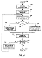
- Fig. 6 is a flowchart outlining one exemplary embodiment of a high addressability image generating method according to this invention.
- the processing process begins in step S100, and continues to step S200, where a normal addressability image, i.e., an observed image, is input.
- step S300 the first pixel in the observed image is selected as the observed or current pixel. Control then passes to step S400.
- step S400 the grayscale value "X" of the current normal addressability pixel is determined. Then, in step S500, a determination is made whether the grayscale value X of the current normal addressability pixel is at most equal to 32. If, in step S500, the grayscale value of the current normal addressability pixel is 32 or less, control continues to step S600. Otherwise, control jumps to step S700. In step S600, a determination is made that no subpixel should be printed for the current pixel. Control then jumps to step S800. In contrast, in step S700, the subpixel to be fired for the current observed pixel is determined. Control then continues to step S800.
- step S800 the error between the output pixel value, which is 255 or 0, depending on whether any of the high addressability subpixels for the current pixel were printed, or if no high addressability pixel was printed, and the grayscale image value of the current pixel is determined and distributed to at least one subsequent observed pixel.
- step S900 a determination is made whether the current observed pixel is the last pixel. This may be a determination whether the current observed pixel is the last pixel in the scan line or in the entire image. If the current pixel in the observed image is not the last pixel, control continues to S1000. Otherwise, control jumps to step S1100. In step S1000, the next pixel is selected as the current observed pixel. Control then returns to S400. In contrast, in step S1100, the process ends.
- Fig. 7 is a flowchart outlining in greater detail one exemplary embodiment of the determination of the location of the printed subpixel within the current observed pixel. Beginning in step S700, control continues to step S710, where the value of S R for the current normal addressability pixel is determined using Eqs. (1) and (2).
- step S720 a determination is made whether the subpixel value for the current normal addressability pixel is sufficiently far enough away from the printed subpixel value of the previous pixel. This can be done using Eqs. (4) and (5), but can also be done any other appropriate way. If, in step S720, the determined subpixel value is sufficiently far enough away, control jumps to step S740. Otherwise control continues to step S730. In step S730, the subpixel value determined in step S720 is adjusted to ensure the subpixel value for the current pixel is sufficiently far enough away. Control then continues to step S740. In step S740, the subpixel location determined in step S710 is fired, i.e., printed. Then, in step S750, control returns to step S800 of Fig. 6 .
- steps S720 and S730 can be omitted, such that control jumps directly from step S710 to step S740.
- the high addressability ink ejection printing system 200 shown in Figs. 2 and 3 is preferably implemented on a programmed general purpose computer. However, the high addressability ink ejection printing system 200 shown in Figs. 2 and 3 can also be implemented on a special purpose computer, a programmed microprocessor or microcontroller and peripheral integrated circuit elements, an ASIC or other integrated circuit, a digital signal processor, a hardwired electronic or logic circuit such as a discrete element circuit, a programmable logic device such as a PLD, PLA, FPGA or PAL, or the like. In general, any device, capable of implementing a finite state machine that is in turn capable of implementing the flowcharts shown in Figs. 6 and 7 , can be used to implement the high addressability ink ejection printing system 200.
- each of the circuits shown in Figs. 2 and 3 can be implemented as portions of a suitably programmed general purpose computer.
- each of the circuits shown in Figs. 2 and 3 can be implemented as physically distinct hardware circuits within an ASIC, or using a FPGA, a PDL, a PLA or a PAL, or using discrete logic elements or discrete circuit elements.
- the particular form each of the circuits shown in Figs. 2 and 3 will take is a design choice and will be obvious and predicable to those skilled in the art.
- the memory 240 is preferably implemented using static or dynamic RAM. However, the memory 240 can also be implemented using a floppy disk and disk drive, a writable optical disk and disk drive, a hard drive, flash memory or any other known or later developed alterable volatile or non-volatile memory device or system.
Landscapes
- Engineering & Computer Science (AREA)
- Physics & Mathematics (AREA)
- Multimedia (AREA)
- General Engineering & Computer Science (AREA)
- General Physics & Mathematics (AREA)
- Theoretical Computer Science (AREA)
- Signal Processing (AREA)
- Mathematical Physics (AREA)
- Image Processing (AREA)
- Facsimile Image Signal Circuits (AREA)
- Ink Jet (AREA)
- Color, Gradation (AREA)
- Fax Reproducing Arrangements (AREA)
- Record Information Processing For Printing (AREA)
Claims (9)
- Procédé de génération de données d'impression à capacité d'adressage élevée disposant d'une capacité d'adressage élevée à partir de données d'image (242) ayant plusieurs pixels d'entrée (243) à une résolution d'entrée qui est inférieure à la résolution à capacité d'adressage élevée, chaque pixel (243) à la résolution d'entrée correspondant à un groupe de sous-pixels (246) à la résolution à capacité d'adressage élevée, comprenant le fait de :introduire, pour un pixel actuel (243) à la résolution d'entrée, des données d'image (242) multi-binaires correspondant au pixel d'entrée actuel (243);caractérisé par le fait de :convertir la valeur de données d'image (242) multi-binaires correspondant au pixel d'entrée actuel (243) en une valeur d'indice (246) qui indique l'unique sous-pixel, parmi le groupe de sous-pixels qui correspond au pixel d'entrée actuel (243), qui doit être marqué (244).dans lequel la valeur d'indice (246) correspondant au pixel d'entrée actuel (243) est déterminée sur la base de la valeur de données d'image (242) multi-binaires, d'une somme de toute partie (260) de valeur d'erreur distribuée (270) au pixel d'entrée actuel (243), d'une valeur seuil et d'un rapport de la résolution à capacité d'adressage élevée à la résolution d'entrée.
- Procédé de la revendication 1, comprenant en plus le fait de :déterminer, pour le pixel actuel (243), une valeur d'erreur (260) entre la valeur de données d'image (242) multi-binaires du pixel d'entrée actuel (243) et une valeur de données d'image (242) multi-binaires marquée déterminée sur la base de la valeur d'indice (246) déterminée ; etdistribuer (270) la valeur d'erreur (260) déterminée à au moins un pixel d'entrée (246) subséquent.
- Procédé de la revendication 2, dans lequel :lorsque la valeur d'indice (243) indique qu'une marque doit être formée dans un premier sous-pixel parmi le groupe de sous-pixels, la valeur de données d'image (242) multi-binaires marquée est équivalente à une valeur de données d'image (242) multi-binaires la plus sombre ; etlorsque la valeur d'indice (243) indique qu'une marque ne doit pas être formée, la valeur de données d'image (242) multi-binaires marquée est équivalente à une valeur de données d'image (242) multi-binaires la plus lumineuse.
- Procédé de la revendication 2, dans lequel, lorsque la valeur d'erreur (260) déterminée doit être distribuée (270) à, au plus, un pixel d'entrée (246) subséquent, la valeur d'erreur (260) déterminée est distribuée (270) à un pixel d'entrée (246) suivant.
- Procédé de la revendication 2, dans lequel, lorsque la valeur d'erreur (260) déterminée est distribuée (270) à plusieurs pixels d'entrée (246) subséquents, chacun des nombreux pixels d'entrée (246) subséquents reçoit une partie de la valeur d'erreur (260) déterminée, la partie de la valeur d'erreur (260) déterminée étant reçue par chacun des nombreux pixels d'entrée (246) subséquents sur la base de la valeur de données d'image (242) multi-binaires du pixel d'entrée actuel (243).
- Procédé de la revendication 5, dans lequel, pour chacun des nombreux pixels d'entrée (246) subséquents, la partie de la valeur d'erreur (260) déterminée distribuée (270) à ce pixel d'entrée (246) subséquent est une fonction de la valeur de données d'image (242) multi-binaires du pixel d'entrée actuel (243).
- Procédé de la revendication 5, dans lequel, pour chacun des nombreux pixels d'entrée (246) subséquents, la partie de la valeur d'erreur (260) distribuée (270) à ce pixel d'entrée (246) subséquent est une fonction de la valeur de données d'image (242) multi-binaires du pixel d'entrée actuel (243).
- Procédé de la revendication 2, dans lequel, lorsque la valeur d'erreur (260) est distribuée (270) à de nombreux pixels d'entrée (246) subséquents, chacun des nombreux pixels d'entrée (246) subséquents reçoit une partie de la valeur d'erreur (260), la partie de la valeur d'erreur (260) étant reçue par chacun des nombreux pixels d'entrée (246) subséquents sur la base d'un ensemble prédéterminé de poids de distribution (270).
- Appareil (200) de génération de données d'impression à capacité d'adressage élevée disposant d'une résolution à capacité d'adressage élevée à partir de données d'image (242) ayant plusieurs pixels d'entrée (246) à une résolution d'entrée, chaque pixel (246) à la résolution d'entrée correspondant à un groupe de sous-pixels (246) à la résolution à capacité d'adressage élevée, comprenant :une interface (100) qui introduit les données d'image ;une mémoire (240) qui stocke au moins les données d'image d'entrée ;un circuit local (250) d'analyse de données d'image ;un circuit (260) de détermination de valeur d'erreur ; etun circuit (270) de distribution d'erreurs,caractérisé en ce que
le circuit local (250) d'analyse de données d'images convertit la valeur de données d'image (242) multi-binaires pour chacun des nombreux pixels d'entrée en une valeur d'indice (243) qui indique l'unique sous-pixel (246), parmi les groupes de sous-pixels qui correspondent aux nombreux pixels d'entrée (246), qui doit être marqué, où la valeur d'indice (246) correspondant à un pixel d'entrée actuel (243) est déterminée sur la base de la valeur de données d'image (242) multi-binaires, d'une somme de toute partie (260) de valeur d'erreur distribuée (270) au pixel d'entrée actuel (243), d'une valeur seuil et d'un rapport de la résolution à capacité d'adressage élevée à la résolution d'entrée.
Applications Claiming Priority (2)
| Application Number | Priority Date | Filing Date | Title |
|---|---|---|---|
| US09/343,529 US6325487B1 (en) | 1999-06-30 | 1999-06-30 | Systems and methods for generating high addressability images |
| US343529 | 1999-06-30 |
Publications (3)
| Publication Number | Publication Date |
|---|---|
| EP1067763A2 EP1067763A2 (fr) | 2001-01-10 |
| EP1067763A3 EP1067763A3 (fr) | 2006-03-08 |
| EP1067763B1 true EP1067763B1 (fr) | 2009-03-25 |
Family
ID=23346484
Family Applications (1)
| Application Number | Title | Priority Date | Filing Date |
|---|---|---|---|
| EP00113728A Expired - Lifetime EP1067763B1 (fr) | 1999-06-30 | 2000-06-28 | Système et procédé pour obtenir des images à haute facilité d'adressage |
Country Status (4)
| Country | Link |
|---|---|
| US (1) | US6325487B1 (fr) |
| EP (1) | EP1067763B1 (fr) |
| JP (1) | JP4350277B2 (fr) |
| DE (1) | DE60041849D1 (fr) |
Families Citing this family (13)
| Publication number | Priority date | Publication date | Assignee | Title |
|---|---|---|---|---|
| DE10211530A1 (de) * | 2002-03-15 | 2003-10-09 | Oce Printing Systems Gmbh | Elektrofotografisches Verfahren und Drucksystem zum Erzeugen eines Druckbildes |
| JP2004209913A (ja) * | 2003-01-08 | 2004-07-29 | Seiko Epson Corp | 印刷制御装置、印刷制御方法、印刷制御プログラム、色変換テーブル作成装置、色変換テーブル作成方法および色変換テーブル作成プログラム |
| US7277201B2 (en) * | 2003-05-28 | 2007-10-02 | Xerox Corporation | Systems and methods for designing digital anamorphic line screens |
| US6953239B2 (en) * | 2003-06-13 | 2005-10-11 | Hewlett-Packard Development Company, L.P. | Printer system and printing method |
| US7036919B2 (en) * | 2003-06-13 | 2006-05-02 | Hewlett-Packard Development Company, L.P. | Print Cartridge |
| JP4424468B2 (ja) * | 2003-09-30 | 2010-03-03 | セイコーエプソン株式会社 | 画像処理装置、画像処理方法、画像処理プログラムおよび印刷制御装置 |
| US8169659B2 (en) * | 2004-02-17 | 2012-05-01 | Xerox Corporation | Systems and methods for reducing a trade-off between image quality and marking speed |
| US7460727B2 (en) * | 2005-06-30 | 2008-12-02 | Xerox Corporation | Error diffusion method and hardware architecture |
| US7565027B2 (en) * | 2005-10-07 | 2009-07-21 | Xerox Corporation | Countdown stamp error diffusion |
| US8351062B2 (en) | 2007-02-26 | 2013-01-08 | Marvell World Trade Ltd. | Bit selection from print image in memory of handheld image translation device |
| TW201103307A (en) * | 2009-07-10 | 2011-01-16 | Shanghai Microtek Technology Co Ltd | Calibrating device, mapping and compensation method for image sensors |
| US8814300B2 (en) | 2012-07-16 | 2014-08-26 | Xerox Corporation | System and method for sub-pixel ink drop adjustment for process direction registration |
| US9215345B2 (en) | 2013-03-26 | 2015-12-15 | Xerox Corporation | Method and system for inverse halftoning utilizing inverse projection of predicted errors |
Family Cites Families (16)
| Publication number | Priority date | Publication date | Assignee | Title |
|---|---|---|---|---|
| FR2587572B1 (fr) * | 1985-03-20 | 1994-02-18 | Canon Kk | Appareil et procede de traitement d'images |
| DE69114581T2 (de) * | 1990-06-27 | 1996-03-28 | Konishiroku Photo Ind | Vorrichtung zur Bilderzeugung. |
| US5608821A (en) | 1994-08-03 | 1997-03-04 | Xerox Corporation | Method of high addressability error diffusion |
| US5696601A (en) | 1994-08-03 | 1997-12-09 | Xerox Corporation | System and method for redistributing error values from an error diffusion process |
| US5528384A (en) | 1994-08-03 | 1996-06-18 | Xerox Corporation | System and method for implementing fast high addressability error diffusion process |
| US5708514A (en) * | 1994-08-31 | 1998-01-13 | Kabushiki Kaisha Toshiba | Error diffusion method in a multi-level image recording apparatus utilizing adjacent-pixel characteristics |
| JPH08237483A (ja) | 1994-12-01 | 1996-09-13 | Xerox Corp | イメージデータを処理するためのシステム及び方法 |
| US5675365A (en) | 1995-09-13 | 1997-10-07 | Xerox Corporation | Ejector activation scheduling system for an ink-jet printhead |
| US5655061A (en) * | 1995-11-15 | 1997-08-05 | Xerox Corporation | System and method for providing a high addressable printing system |
| US5933539A (en) | 1996-05-30 | 1999-08-03 | Xerox Corporation | Method and system for hybrid error diffusion processing of image information using programmable screen modulation |
| US5787206A (en) | 1996-05-30 | 1998-07-28 | Xerox Corporation | Method and system for processing image information using expanded dynamic screening and error diffusion |
| US5903361A (en) | 1996-06-06 | 1999-05-11 | Xerox Corporation | Method and system for processing image information using background error diffusion |
| US5809177A (en) | 1996-06-06 | 1998-09-15 | Xerox Corporation | Hybrid error diffusion pattern shifting reduction using programmable threshold perturbation |
| US5748785A (en) | 1996-09-26 | 1998-05-05 | Xerox Corporation | Inter-separation color image processing using error diffusion |
| US5974228A (en) * | 1997-01-28 | 1999-10-26 | Hewlett-Packard Company | Image rendition by plural-row error diffusion, for faster operation and smaller integrated circuits |
| US6020979A (en) * | 1998-03-23 | 2000-02-01 | Xerox Corporation | Method of encoding high resolution edge position information in continuous tone image information |
-
1999
- 1999-06-30 US US09/343,529 patent/US6325487B1/en not_active Expired - Lifetime
-
2000
- 2000-06-26 JP JP2000190357A patent/JP4350277B2/ja not_active Expired - Fee Related
- 2000-06-28 DE DE60041849T patent/DE60041849D1/de not_active Expired - Lifetime
- 2000-06-28 EP EP00113728A patent/EP1067763B1/fr not_active Expired - Lifetime
Also Published As
| Publication number | Publication date |
|---|---|
| DE60041849D1 (de) | 2009-05-07 |
| JP2001053971A (ja) | 2001-02-23 |
| JP4350277B2 (ja) | 2009-10-21 |
| EP1067763A2 (fr) | 2001-01-10 |
| US6325487B1 (en) | 2001-12-04 |
| EP1067763A3 (fr) | 2006-03-08 |
Similar Documents
| Publication | Publication Date | Title |
|---|---|---|
| US11477343B2 (en) | Dynamic printing system compensation mechanism | |
| US5404411A (en) | Bitmap-image pattern matching apparatus for correcting bitmap errors in a printing system | |
| US6252675B1 (en) | Apparatus and method for halftone hybrid screen generation | |
| EP0260020A2 (fr) | Procédé pour générer une image à échelle de gris | |
| EP0889639B1 (fr) | Rendu de demi-teintes à plusieurs niveaux avec contours à texture réduite et commande de recouvrement | |
| EP1067763B1 (fr) | Système et procédé pour obtenir des images à haute facilité d'adressage | |
| US6332666B1 (en) | Printing apparatus, resolution conversion printing method for printing apparatus, and storage medium storing computer-readable program | |
| EP0768792A2 (fr) | Procédé et appareil pour l'amélioration de la résolution des images à échelle de gris qui comporte du texte et des images | |
| EP0843232B1 (fr) | Appareil pour générer des données d'impulsions en durées pour un appareil d'impression du type de transfert de toner | |
| EP0796002B1 (fr) | Procédé d'amélioration de la qualité d'impression d'une imprimante avec au moins une résolution supérieure dans une direction | |
| US6301397B1 (en) | Systems and methods for rotating high addressability images | |
| EP1017018B1 (fr) | Procédé et appareil pour la rotation d'image à haute facilité d'adressage | |
| EP0457511B1 (fr) | Appareil pour la génération d'une reproduction tramée d'une image | |
| US7315398B2 (en) | Multi-level error diffusion with color image data | |
| EP0893780B1 (fr) | Méthode de conversion de résolution de données d'impression pour une imprimante | |
| EP1439690B1 (fr) | Processeur demi-tons avec sortie multi-bit échantillonée pour matrice de seuils | |
| US5689344A (en) | Mitigation of tenting deletions in color xerographic printers | |
| US7295347B2 (en) | Image processing method for generating multi-level data | |
| US5227895A (en) | Method and apparatus for image reproduction | |
| JP3495406B2 (ja) | 画像形成装置 | |
| EP1096784B1 (fr) | Réduction de motif d'interférence Moiré pendant le balayage d'images en demi-teinte | |
| CA2129090C (fr) | Appareil et methode de filtrage d'images pour la reproduction | |
| CA2128995C (fr) | Microsegmentation dans une imprimante | |
| US6049395A (en) | Method and system for achieving enhanced gray levels in a screen cell array | |
| EP0667705A1 (fr) | Procédé et appareil pour générer une reproduktion tramée d'une image |
Legal Events
| Date | Code | Title | Description |
|---|---|---|---|
| PUAI | Public reference made under article 153(3) epc to a published international application that has entered the european phase |
Free format text: ORIGINAL CODE: 0009012 |
|
| AK | Designated contracting states |
Kind code of ref document: A2 Designated state(s): AT BE CH CY DE DK ES FI FR GB GR IE IT LI LU MC NL PT SE |
|
| AX | Request for extension of the european patent |
Free format text: AL;LT;LV;MK;RO;SI |
|
| PUAL | Search report despatched |
Free format text: ORIGINAL CODE: 0009013 |
|
| AK | Designated contracting states |
Kind code of ref document: A3 Designated state(s): AT BE CH CY DE DK ES FI FR GB GR IE IT LI LU MC NL PT SE |
|
| AX | Request for extension of the european patent |
Extension state: AL LT LV MK RO SI |
|
| 17P | Request for examination filed |
Effective date: 20060908 |
|
| AKX | Designation fees paid |
Designated state(s): DE FR GB |
|
| 17Q | First examination report despatched |
Effective date: 20061107 |
|
| GRAP | Despatch of communication of intention to grant a patent |
Free format text: ORIGINAL CODE: EPIDOSNIGR1 |
|
| GRAS | Grant fee paid |
Free format text: ORIGINAL CODE: EPIDOSNIGR3 |
|
| GRAA | (expected) grant |
Free format text: ORIGINAL CODE: 0009210 |
|
| AK | Designated contracting states |
Kind code of ref document: B1 Designated state(s): DE FR GB |
|
| REG | Reference to a national code |
Ref country code: GB Ref legal event code: FG4D |
|
| REF | Corresponds to: |
Ref document number: 60041849 Country of ref document: DE Date of ref document: 20090507 Kind code of ref document: P |
|
| PLBE | No opposition filed within time limit |
Free format text: ORIGINAL CODE: 0009261 |
|
| STAA | Information on the status of an ep patent application or granted ep patent |
Free format text: STATUS: NO OPPOSITION FILED WITHIN TIME LIMIT |
|
| 26N | No opposition filed |
Effective date: 20091229 |
|
| REG | Reference to a national code |
Ref country code: FR Ref legal event code: PLFP Year of fee payment: 17 |
|
| PGFP | Annual fee paid to national office [announced via postgrant information from national office to epo] |
Ref country code: GB Payment date: 20160527 Year of fee payment: 17 Ref country code: DE Payment date: 20160524 Year of fee payment: 17 |
|
| PGFP | Annual fee paid to national office [announced via postgrant information from national office to epo] |
Ref country code: FR Payment date: 20160526 Year of fee payment: 17 |
|
| REG | Reference to a national code |
Ref country code: DE Ref legal event code: R119 Ref document number: 60041849 Country of ref document: DE |
|
| GBPC | Gb: european patent ceased through non-payment of renewal fee |
Effective date: 20170628 |
|
| REG | Reference to a national code |
Ref country code: FR Ref legal event code: ST Effective date: 20180228 |
|
| PG25 | Lapsed in a contracting state [announced via postgrant information from national office to epo] |
Ref country code: DE Free format text: LAPSE BECAUSE OF NON-PAYMENT OF DUE FEES Effective date: 20180103 Ref country code: GB Free format text: LAPSE BECAUSE OF NON-PAYMENT OF DUE FEES Effective date: 20170628 |
|
| PG25 | Lapsed in a contracting state [announced via postgrant information from national office to epo] |
Ref country code: FR Free format text: LAPSE BECAUSE OF NON-PAYMENT OF DUE FEES Effective date: 20170630 |