EP1081741A2 - Focusing method and system - Google Patents
Focusing method and system Download PDFInfo
- Publication number
- EP1081741A2 EP1081741A2 EP00118880A EP00118880A EP1081741A2 EP 1081741 A2 EP1081741 A2 EP 1081741A2 EP 00118880 A EP00118880 A EP 00118880A EP 00118880 A EP00118880 A EP 00118880A EP 1081741 A2 EP1081741 A2 EP 1081741A2
- Authority
- EP
- European Patent Office
- Prior art keywords
- specimen
- signal
- charged particle
- parameter
- scoring
- Prior art date
- Legal status (The legal status is an assumption and is not a legal conclusion. Google has not performed a legal analysis and makes no representation as to the accuracy of the status listed.)
- Withdrawn
Links
Images


Classifications
-
- H—ELECTRICITY
- H01—ELECTRIC ELEMENTS
- H01J—ELECTRIC DISCHARGE TUBES OR DISCHARGE LAMPS
- H01J37/00—Discharge tubes with provision for introducing objects or material to be exposed to the discharge, e.g. for the purpose of examination or processing thereof
- H01J37/02—Details
- H01J37/21—Means for adjusting the focus
-
- H—ELECTRICITY
- H01—ELECTRIC ELEMENTS
- H01J—ELECTRIC DISCHARGE TUBES OR DISCHARGE LAMPS
- H01J2237/00—Discharge tubes exposing object to beam, e.g. for analysis treatment, etching, imaging
- H01J2237/21—Focus adjustment
- H01J2237/216—Automatic focusing methods
Definitions
- the invention relates to methods for automatic focusing a charged particle beam. Furthermore, this invention relates to autofocus of a charged particle beam under conditions of charge on the examined specimen.
- the charged particle beam In order to get a sharp and clear picture of the specimen, it is necessary to focus the charged particle beam on the specimen. Due to the fact that most specimen show some variation in their surface height, the charged particle beam has to be refocused from time to time so that a certain image quality is maintained.
- the focusing of the charged particle beam is usually done by either varying the current supplied to the objective lens, and thereby changing the focal length, or changing the working distance to the specimen using a Z-stage.
- USP 4,999,496 recognizes that changes in focal length or working distance also cause changes in the magnification. In order to compensate for changes in magnification, it teaches to change the beam voltage until a focus is achieved, and use the amount of change to compensate for the changes in magnification.
- the electric potential on the surface of the specimen may be caused by an unintentional or unavoidable charging of the specimen.
- the electric potential on the surface of the specimen may also be caused by intentionally applying a voltage to the specimen.
- a voltage can be applied to a wafer, for example, in order to obtain voltage contrast imaging which is used to detect shorts in a circuit.
- Some specimen like for example semiconductor wafers, contain a plurality of different target areas that have to be examined. Due to the fact that most specimen are warped and that they usually exhibit some undulations in their surface height, it is often necessary to refocus the charged particle beam on each target area. Unfortunately, this refocusing of the charged particle beam on each target area is a rather time consuming operation.
- One commonly used way is to focus an optical system on each target area and to learn each target area height. Once each target area height is known, the electron beam can be driven to the right focus on a specific target area if the function of electron beam focus versus the target area height is known.
- the process described above leads to additional disadvantages.
- the transparency of the target area may lead to significant errors in the focusing of the electron beam because the optical system may measure the target area height incorrectly. Furthermore, an electric potential being present in the target area will usually lead to a serious degradation of the image quality. Accordingly, there is also a need for a faster and more reliable method for focusing a beam, especially a charged particle beam, onto a target area.
- Prior art methods for focusing a charged particle beam often require a definition of a focus search range for the focus setting and than form corresponding image signals in different focus states of the beam in a way that the focus search range is covered. Focus scores are computed for every image and the scores of all the images are then compared. The value of the parameter corresponding to the image having the highest score is selected for the actual measurement.
- the predetermined search range does not include the best focus state and therefore the prior art approach is not capable of finding the best focus state.
- a lot of time is usually wasted, because image signals have to be formed throughout the whole search range. Accordingly, there is also a need for a faster method for focusing a charged particle beam, that does not require a predetermined search range.
- the present invention provides a method for automatic focusing a charged particle beam, which compensates for both surface topography and electric charge on the specimen.
- "global" focusing is done using a Z-stage, while correction, especially for charge, are made by changing the beam energy.
- a fast response is provided for charging effects, while avoiding changes in magnification or scanning direction.
- the negative effects of an electric potential being present on the surface of the specimen are overcome by analyzing scores of images achieved with different beam energies and by adjusting the beam energy according to the analysis.
- image quality problems caused, for example, by a wafer charged with a static charge and showing a surface potential in the range of a couple of hundreds volts, for example + 100 to ⁇ 400 V, can be corrected without any image rotation.
- stigmation or other beam alignments there is no necessity to correct stigmation or other beam alignments.
- the magnification remains constant. Accordingly, there is no need to provide a magnification compensation.
- the present invention also provides an apparatus for the examination of specimen that is capable of performing this improved method.
- the present invention provides a method for mapping a charge distribution on the surface of a specimen.
- the method uses the information contained in the corrections, that are made by changing the beam energy, in order to compensate for electric charge on the specimen.
- the beam energy or the changes to the beam energy together with the coordinates of the scanned location are recorded, so that a map showing the charge distribution and/or the field distribution on the surface of the specimen can be constructed.
- Such a map can be of very high value, for example, when a failure in a circuit design has to be found.
- the present invention also provides an apparatus for providing a map of the charge distribution on the surface of a specimen.
- the present invention provides an improved method for focusing a beam onto a target area of a specimen.
- the method uses images of a repeating pattern that lies in the path of the beam on its way to the actual target area. Scores of these images that are achieved with different focus settings are analyzed and the correct focus setting is then used once the beam has reached the target area.
- This method has the advantage that the information about the correct focus is gathered during the time period in which the specimen and/or the beam is moved to the actual target location. Furthermore, this is done through an analysis of the information obtained by the images created by the beam itself.
- the beam is basically in focus when it reaches the target area. Accordingly, a lot of time, that usually has to be used for collecting all the information about the surface height of each target area, can be saved and the throughput is increased.
- the present invention also provides an apparatus for the examination of specimen that is capable of performing this improved focusing method.
- the present invention provides a further improved method for automatic focusing a charged particle beam.
- the method uses the image scores of two successive focus states and changes the focus state then in a direction that will yield an improvement in the scores. This is repeated until the score has reached a predetermined value or the changes in the scores (or in the focus states) are smaller than a predetermined value that is, for example, smaller or equal to the depth of focus of the beam.
- the method has the advantage that there is no need to define the focus search range in advance and the method in most cases converges much faster than the methods used in the prior art.
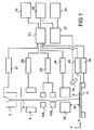
- a first embodiment according to the invention is shown schematically in Fig. 1.
- An electron beam 4 is emitted from the electron source 2 e.g. a tungsten-hairpin gun, a lanthanum-hexaboride gun, or a field-emission gun.
- the electron source is supplied by a high voltage supply unit.
- the electron source 2 is followed by a condenser lens 5, which demagnifies the beam and guides the beam towards a specimen 8.
- the beam 4 of charged particles then enters the scanning coils 12A and 12B, which are used to move the electron beam 4 over a target area on the specimen 8.
- the scanning coils 12A and 12B are followed by the objective lens 10 for focusing the particle beam 4 onto a specimen 8, which is located on the specimen support 11.
- the objective lens can be magnetic or electrostatic.
- the specimen support 11 is capable of moving the specimen 8 in all directions.
- the electrons strike the surface of the specimen 8, they undergo a series of complex interactions with the nuclei and electrons of the atoms of the specimen.
- the interactions between the incident electron and the atoms of the specimen may be elastic or inelastic.
- the interactions produce a variety of secondary products, such as electrons of different energy, X rays, light, and heat, as well as electrons scattered backward. Many of these secondary products and/or the backscattered charged particles are used to produce the image of the specimen and to collect additional data from the specimen 8.
- a secondary product of major importance to examination or the image formation of specimens are secondary electrons that escape from the specimen 8 at a variety of angles with relatively low energy (3 to 50 eV). These secondary electrons reach the detector 16 and are detected. By scanning the electron beam 4 over the specimen 8 and displaying/recording the output of the detector 16 an image of the surface of the specimen 8 is formed.
- the different parts of the apparatus are connected to corresponding supply units, the high voltage supply unit 21, the condenser lens supply unit 22, the scanning coil supply unit 23, the objective lens supply unit 24, the specimen voltage supply unit 25 and the stage supply unit 26, which are controlled by the parameter adjustment unit 31.
- the parameter adjustment unit 31 is connected with the standard setting unit 35, which provides a basic set of parameters to the parameter adjustment unit 31.
- the objective lens supply unit 24 controls the objective lens according to parameters supplied by the parameter setting unit 35, so that the lens focuses the electron beam on the surface of the specimen 8.
- the parameters are selected according to an autofocus system (not shown) that is per se known in the art, and focuses the beam according to the topography of the specimen.
- the specimen may, for example, be unintentionally charged with a static charge and may exhibit a surface potential, for example in the range of + 100 to ⁇ 400V. This problem is exacerbated by the fact that the charge on the sample changes as the sample is scanned for imaging. So while the focus may be adjusted to obtain optimal image of an uncharged sample, as the sample is scanned for imaging it gets increasingly charged and the focus changes and the image is degraded.
- the electric potential on the surface of the specimen may also be caused by intentionally applying a voltage to the specimen 8.
- the parameter adjustment unit 31 generates a signal to the specimen voltage supply unit 25, which applies a corresponding voltage to the specimen support 11 and specimen 8.
- the voltage applied to the specimen 8 can be used, for example, to filter out those secondary electrons that have less than a certain energy, or to assist secondary electrons escape high aspect features, such as holes and vias.
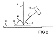
- Fig. 2 exemplifies the effects of a positive potential applied to the specimen 8, thereby creating an electrons attractive field.
- the electron beam 4 hits the specimen 8 and secondary electrons escape from the surface of the specimen 8 at a variety of angles with relatively low energy (3 to 50 eV).
- Those secondary electron 6 that have less than a predetermined energy, e.g. 20 V, are not capable of escaping the attractive field and reach the detector 16. Consequently, they follow a curved path back to the specimen 8. Only those secondary electrons 7 that have more than the predetermined energy will escape the resulting attractive field and reach the detector 16. Accordingly, the positive voltage applied to the specimen 8 can be used to filter out those secondary electrons that have less than a predetermined energy.
- a repelling field is created that assists the electrons escaping the sample.
- the voltage supplied to the specimen may also be used in order to obtain voltage contrast imaging. Voltage contrast imaging is often used to detect shorts in a circuit produced on a semiconductor wafer.
- an electric potential present on the surface of the specimen does also effect the electron beam 4.
- the effects on the electron beam 4 usually results in a degradation of the image quality. Specifically, when the potential on the specimen 8 changes, the image is distorted as being out of focus.
- the parameters of the objective lens are set according to the surface topography.
- an additional autofocus output is used to vary the beam energy so as to compensate for specimen charge. That is, the objective lens is set to a general focus setting, while the beam energy is controlled to compensate for changes in focus settings due to surface topology or specimen charge. In this manner, "fine" tuning of the focal point of the beam can be rapidly performed since the lens operating parameters remain constant. Additionally, changes in the beam energy, while compensating for focus changes, do not result in image rotation. Moreover, since the change in beam energy is equivalent to the amount of charge on the specimen, no change in magnification occurs, and there is no need to compensate for magnification changes.
- the autofocus is first used to determine a basic focus parameter for the objective lens and/or Z-stage. Then the lens parameters are fixed, and any changes dictated by the autofocus system are translated into beam energy changes.
- One advantageous embodiment utilizing such a beam-energy focusing will now be described.
- the objective current is set constant to focus the beam at a predetermined working distance.
- An optical autofocus system (not shown) is used to map the topography of the specimen, or selected targets thereupon.
- Such optical autofocus systems are well known in the art. For example, one such system is incorporated in the global pre-aligner of the CD-SEM 9000Si system available from Applied Materials for Santa Clara, Ca.
- Another optical autofocus which measures the elevation of the sample at a point under the electron beam is disclosed in USP 5,311,288. Any of such systems can be used so as to bring the inspected surface to the appropriate working distance that is at the focus point of the objective.
- the specimen support 11 (Z-stage) driven by the stage supply unit 26 is used to bring each location/target to the appropriate working distance W from the objective.
- each location/target on the specimen is brought into focus under the objective.
- small errors can always be introduced into the autofocus system and Z-stage. These small errors are corrected using changes in the beam energy. The following is an example of one method for making these small adjustments.
- the analyzing unit 32 causes the parameter adjustment unit 31 to transmit a corresponding signal to the scanning coil supply unit 23, so that the electron beam scanned over the specimen or a predetermined portion thereof.
- the electron beam hits the specimen 8 and secondary electrons coming from the specimen 8 are detected by the detector 16. Accordingly, an image signal is produced and the image signal is transmitted to scoring unit 33, which scores the images in order to determine the quality of the images.
- the resulting scores are sent to the analyzing unit 32, which after a predetermined time interval, causes the parameter adjustment unit 31 to generate a beam energy changing signal.
- the voltage supply unit 21 increases the accelerating voltage by a predetermined amount and maintains this new accelerating voltage until a further beam energy changing signal arrives.
- the analyzing unit 32 causes the parameter adjustment unit 31 to transmit a corresponding signal to the scanning coil supply unit 23, so that electron beam repeats its motion over the specimen.
- the detector 16 continues to measure the secondary electrons coming from the surface of the specimen, so that an image signal is produced.
- the scoring unit 33 continues to score the image signal and sends the scores to the analyzing unit 32.
- the analyzing unit 32 causes the parameter adjustment unit 31 again to generate beam energy changing signal.
- the voltage supply unit 21 decreases the accelerating voltage by a predetermined amount and maintains this new accelerating voltage until a further beam energy changing signal arrives.
- the analyzing unit 32 causes the parameter adjustment unit 31 again to transmit a corresponding signal to the scanning coil supply unit 23, so that electron beam repeats its motion over the specimen.
- the analyzing unit 32 By scoring the resulting image signal for the last time interval and sending the results to the analyzing unit 32, the analyzing unit 32 has enough information to compute a value for the beam energy, so that the electric potential being present on the specimen 8 is compensated. The analyzing unit 32 will then cause the parameter adjustment unit 31 to generate beam energy changing signal, so that the correct beam energy will be used for the following measurement.
- the accelerating voltage is varied within a few ten volts ( ⁇ ), for example ⁇ 60 Volts, of a nominal value, provided by the parameter setting unit 35. Such small changes cause negligible changes in magnification.
- the analyzing unit 32 may cause the parameter adjustment unit 31 to change the beam energy in predetermined steps and the corresponding images are stored in the scoring unit 33 before the actual scoring is performed. After the scoring unit 33 has scored the stored images, the scores are transferred to the analyzing unit 32. The analyzing unit 32 then has enough information to compute a value for the beam energy, so that the electric potential being present on the specimen 8 is compensated. The analyzing unit 32 will then cause the parameter adjustment unit 31 to generate beam energy changing signal, so that the correct beam energy will be used for the following measurement.
- a variety of methods can be used.
- a preferred method to score the quality of an image is described with reference to Figs. 3 and 4.
- Some specimen 8 for example semiconductor wafers, exhibit sharp feature edges on their surface.
- the preferred scoring method scores the quality of an image based on the sharpness of that part of the image that represents the feature edge. Obviously, the highest scores are given those image that show the feature edge as sharp as possible.
- Fig. 3 shows a situation when the electron beam is moved over a single edge 48 of an aluminum wiring 47 present on top of a SiO 2 -layer 49.
- the electron beam is moved from a position I to a position III via an intermediate position II.
- the entire electron beam does not hit the edge 48 of the aluminum wiring 47. Due to fact that secondary electrons can only escape from a small area near the surface of the die, only a few secondary electron are emitted from the surface of the die.
- the electron beam hits the edge 48 of the aluminum wiring 47. Due to vertical surface of the edge 48, the surface area from which secondary electrons are able to escape is enlarged. Accordingly, the number of secondary electrons, that are emitted from the surface of the die, is increased.
- the entire electron beam hits the flat surface of the aluminum wiring 47 and the number of secondary electrons is reduced. Due to the fact that different materials exhibit different secondary emission efficiencies, the collected signal at the detector varies according to different materials. Since aluminum has a higher secondary emission efficiency than SiO 2 , the number of secondary electron at position III is higher than the number of secondary electrons at position I.
- Fig. 4 is a graph illustrating this variation of the current I S representative of the number of secondary electrons while moving from the position I to the position III via the intermediate position II.
- the graph I S shown in Fig. 4 is intended to describe general aspects of the detected signal like edge enhancement and material contrast.
- the actual shape of the graph I S depends on a plurality of parameters and may differ from the shape of the graph I S shown in Fig. 4.
- the precise shape of the graph I S depends on the spot size of the electron beam and the spot size of the electron beam basically determines the image quality.
- a smaller spot size leads to an image of higher quality, especially to an image of higher resolution.
- the sharpness of the graph I S can be scored, for example, by examining the first derivative of the graph I S or by using the Fourier transform of the graph I S , which yields the weight of high frequencies corresponding to sharp edges.
- specimen voltage supply unit is used to apply a potential to the specimen.
- a corresponding potential is also added to the beam energy by the high voltage supply unit 21, such that the potential between the tip and the specimen remains constant.
- Another advantageous feature of the present invention is providing mapping of charging on a specimen.
- the specimen such as a semiconductor wafer
- the specimen may be charged beforehand by various unrelated processes. It is very desirable to be able to analyze the distribution of the charging over the surface.
- the ability to map charging on the specimen surface can assist in testing the devices manufactured on the wafer. For example, the application and mapping of charge on the wafer can assist in investigation of the performance of the device and identification of faults such as shorts and disconnects.
- the specimen is brought to the appropriate working distance and the voltage suppliers 21 and 24 are set to the standard operation potentials. Then the surface of the specimen is scanned, while the analyzing unit 32 continuously cause the parameter adjustment unit 31 to change the beam energy so that each scanned location is in best focus. The amount of change in the beam energy from the standard operation is then recorded with the corresponding coordinates of the imaged location. From this data, a charge distribution map is constructed. Since the resolution of the SEM is very high, the charge distribution map can be made up to micron accuracy. It should be appreciated that when no auxiliary bias is applied to the sample the SEM is adjusted so that the yield is 1, i.e., the standard beam energy is adjusted so that the number of electron entering and leaving the sample is about the same.
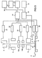
- Fig. 5 shows a block diagram of an apparatus corresponding to this aspect of the present invention. This embodiment is similar to that of Figure 1, except for the following.
- a recording unit 37 is provided in addition to analyzing unit 32.
- the recording unit 37 is connected with the analyzing unit 32, in order to store for each scanned location the beam energy or the changes of the beam energy together with the coordinates of the scanned location.
- the scanned locations may result from a predetermined subdivision of a target area on the specimen or the scanned locations may correspond to features present on the surface of the specimen.
- the analyzing unit 32 determines the correct beam energy so that scanned location is in focus. This information together with the coordinates of the scanned location is then sent to the recording unit 37, so that map of the charge distribution can constructed.
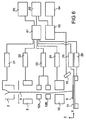
- Fig. 6 shows a block diagram of an apparatus according to a still further aspect of the present invention.
- This embodiment is also similar to that of Figure 1, except for the following.
- the high voltage supply unit 21, the condenser lens supply unit 22, the scanning coil supply unit 23, the objective lens supply unit 24, the specimen voltage supply unit 25, and the stage supply unit 26 are now controlled by the parameter adjustment unit 61.
- the parameter adjustment unit 61 is connected with the standard setting unit 65, which provides, based on the measurement requirements, a basic set of parameters to the parameter adjustment unit 61.
- the values of the parameters, like beam energy, condenser lens current and objective lens current, provided by the standard setting unit 65 are used as starting values, which may then be changed in the process of focusing the electron beam on the different target areas of the specimen 8.
- the parameter adjustment unit 61 is connected with the analyzing unit 62, so that, based on the analysis performed by the analyzing unit 62, the parameters of the apparatus can be adjusted to get a good performance.
- the analyzing unit 62 is also connected to the scoring unit 63, which receives the image signal from the detector 16.
- the scoring unit 63 modifies the image signal, so that the image signal can be displayed on the computer screen 64.
- the scoring unit 63 examines and scores at least portions of the image signal, so that quality of the image signal can be determined by the analyzing unit 62 based on scores provided by the scoring unit 63.
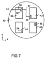
- Fig. 7 shows a schematic view of a semiconductor wafer 40 carrying only four dies 42, 43, 44, 45.
- the dies contain the structures, for example a predetermined part of the metallization, that have to be examined in order to control the quality of the process used to prepare the structures. Accordingly, each die contains a target area 52, 53, 54, 55, in which, for example, the dimensions of an aluminum wiring have to be determined.
- the beam 4 may also be used for a defect review, where the beam 4 (or the stage 11) is the driven from defect to defect which are located randomly over the surface of the wafer.
- the electron beam is moved from a starting point 51 on the wafer to the first target area 52 along a path 56. After the measurement has been completed in the first target area 52, the electron beam is moved to the second target area 53 and so on until all the measurements are completed.
- This movement of the electron beam is achieved by keeping the electron beam directed to a fixed spot (spot mode) and moving the wafer relative to the electron beam. The movement of the wafer is caused by a corresponding movement of the stage 11 in X or Y direction.
- the electron beam may also perform a scanning movement with regard to wafer (scanning mode) while the wafer is held in the correct position. A combined movement of the stage 11 and the beam 4 may also be utilized.
- an optical distance measurement unit is used to measure the surface height of each target area. This information would then be transferred to the standard setting unit 65 so that a standard setting of parameters can be determined for each target area. This process takes place before the actual measurement begins and adds a considerable time delay to the whole measurement process. In the following it is explained how this time delay can be avoided.
- feature edges for example edges of a dielectric layer, edges of a photoresist layer or edges of a metallization, can be used as a repeating pattern in order to score the focusing properties of the electron beam.
- those feature edges are used which extend perpendicular to movement of the electron beam.
- Feature edges present on a semiconductor wafer have the advantage that all feature edges of a certain type, for example the edges of a metallization, basically have the same dimensions. Accordingly, by moving the electron beam over two spaced apart feature edges of the same kind, basically the same image signal is produced. If the focusing properties of the electron beam are changed while moving from one feature edge to the other feature edge, different image signals are produced. However, due to the fact, that these differences in the image signals are only caused by the changed focusing properties, the correct beam focus can be determined.
- Fig. 7 shows a situation when the electron beam is moved over several edges of the aluminum wires 47A, 47B, 47C along its path 56. Thereby, the electron beam 4 is moved from the left to the right. As explained with regard to Fig. 3, every time the electron beam 4 moves over an edge the number of secondary electrons increases.
- Fig. 8 is a graph illustrating this variation of the current I S representative of the number of secondary electrons while moving the electron beam 4 over the aluminum wires 47A, 47B, 47C.
- the value of at least one parameter affecting the focusing properties of the beam is changed.
- the beam energy is changed in order to affect the focusing properties of the electron beam.
- the objective lens current, the position of the stage 11 in Z direction or the potential of the wafer 8 may also be changed, in order to affect the focusing properties of the electron beam.
- the electron beam 4 moves with a predetermined beam energy over the aluminum wire 47A.
- the resulting current of secondary electrons is shown below in Fig. 9.
- the beam energy or, e.g., the lens current
- an increase in the beam energy or objective lens current leads to a decrease in the spot size of the electron beam 4 hitting the wafer.
- the electron beam 4 now moves over the wire 47B with a smaller spot size than before.
- the resulting current of secondary electrons is again shown below in Fig. 9. It can be seen that a smaller spot size of the electron beam 4 leads to a sharper graph I S .
- the beam energy is decreased. Accordingly, the electron beam 4 now moves over the wire 47C with a large spot size and the width of the peaks of the graph I S is increased.
- the change in the beam energy results in a different shape of the graph I S , which, accordingly, leads to a different score for sharpness of graph.
- the direction of the focusing error can be determined. If a change of the beam energy in the positive direction (higher beam energy) leads to a graph having a higher score than a change of the beam energy in the negative direction (lower beam energy), it means that the value of the beam energy has to be changed in the positive direction, in order to focus the electron beam onto the target area.
- the differences in the scores not only the direction of the error but also the magnitude of the error function can be calculated.
- the parameter e.g. beam energy, objective lens current, height of stage, etc
- the parameter e.g. beam energy, objective lens current, height of stage, etc
- the scores of all the image signals are then compared and the value of the parameter corresponding to the image signal having the highest score is selected for the actual measurement.
- the standard setting unit 65 provides a basic set of parameters to the parameter adjustment unit 61. Accordingly, the parameter adjustment unit 61 transmits corresponding signals to the high voltage supply unit 21, the condenser lens supply unit 22, and the objective lens supply unit 24, so that a default accelerating voltage, a default condenser lens current and a default objective lens current is used. Furthermore, the parameter adjustment unit 61 transmits corresponding signals to the scanning coil supply unit 23 and the stage supply unit 26, so that the electron beam directed to a fixed spot (spot mode) and the stage 11 moves the wafer from a starting point to a position corresponding to the first target area.
- the electron beam 4 hits the wafer and secondary electrons coming from the wafer are detected by the detector 16. Accordingly, an image signal is produced and the image signal is transmitted to scoring unit 63, which scores the portion of the image signal that belong to edges in aluminum wiring as has been described above.
- the resulting scores are sent to the analyzing unit 62, which after a predetermined time interval, for example 200 ⁇ sec, causes the parameter adjustment unit 61 to generate beam energy changing signal. Based on the beam energy changing signal the voltage supply unit 61 increases the accelerating voltage by a predetermined amount and maintains this new accelerating voltage until a further beam energy changing signal arrives.
- the detector 16 continues to measure the secondary electrons coming from the surface of the wafer, so that an image signal is produced.
- the scoring unit 63 continues to score the portion of the image signal that belong to edges in aluminum wiring sends the scores to the analyzing unit 62. After further 200 ⁇ sec the analyzing unit 62 causes the parameter adjustment unit 61 again to generate beam energy changing signal. Based on the beam energy changing signal the voltage supply unit 21 decreases the accelerating voltage by a predetermined amount and maintains this new accelerating voltage until a further beam energy changing signal arrives.
- the analyzing unit 62 By scoring the resulting image signal for another 200 ⁇ sec and sending the results to the analyzing unit 62, the analyzing unit 62 usually has enough information to compute a value for the beam energy or for any other parameter affecting the focusing properties of the beam, so that the electron beam is correctly focused onto the first target area 52 when the electron beam reaches the first target area 52.
- the analyzing unit 62 will then cause the parameter adjustment unit 61 to generate beam energy changing signal (or e.g. an objective lens current changing signal), so that the correct beam energy (or e.g. the correct objective lens current) will be used for the following measurement in the first target area 52.
- beam energy changing signal or e.g. an objective lens current changing signal
- the electron beam is moved to the second target area 53, whereby the described method will be repeated and the first target area 52 will now be used as a starting point.
- the beam 4 may use a path that primarily extends over the second die 43.
- the beam 4 may also use the path 57 that primarily extends over the area between the dies 42 and 43.
- This area usually called scribe line, also contains a large number of structures or features, like test circuits or alignment marks, so that feature edges can again be used as a repeating pattern in order to score the image signal.
- Fig. 10 shows a flow chart of a further improved method for automatic focusing a charged particle beam.
- This method can be used to focus a charged particle beam while the beam scans over the actual target area. Furthermore, this method can also be used to focus a charged particle beam while the beam is on its way to the actual target area, like in the preceding example.
- the method starts with a predetermined parameter setting that is adapted to the specific measurement needs.
- the charged particle beam is then moved over the specimen and at least one secondary product and/or backscattered particles coming from the specimen are measured to produce a first signal (Step a).
- the first signal is scored (Step b) and the value of at least one parameter affecting the focusing properties of the beam is changed by a predetermined amount ⁇ (Step c).
- Suitable parameters include the beam energy, the objective lens current, the height of the specimen support or the voltage supplied to the specimen.
- the beam is once again moved over the specimen and a second signal is produced (Step d). This signal is also scored (Step e).
- the difference of the two scores is calculated and the amount ⁇ is chosen to be proportional to this difference (step f). Furthermore, the amount ⁇ by which the value of the parameter is changed in step c is adapted. The amount ⁇ is also chosen to be proportional to the difference of the two scores. In a preferred embodiment these proportionality's are chosen in such a manner that the amount ⁇ is always smaller than the amount ⁇ .
- Steps a, b, c, d, e and f are now repeated (step g) until the difference of the two scores (steps b and e) is less than a predetermined value ⁇ , that is, for example, smaller or equal to the depth of focus of the beam. Once the difference of the two scores is less than depth of focus of the beam, the correct focus setting has been found and the charged particle beam is now focused on the specimen.
- the changes ⁇ and ⁇ are applied to the same parameter, for example the beam energy.
- the change ⁇ is applied to the chosen parameter before the decision (Step g), whether or not the correct focus has been reached, is made.
- the change ⁇ may also be applied to the parameter after this decision has been made.
- the new method is used to focus a charged particle beam while the beam is moved to the actual target area the whole process is repeated until the actual target is reached.
- the parameter values that have been determined during one run of the method are used as starting values for the successive run.
- the method has the advantage that there is no need to define the focus search range in advance and the method in most cases converges much faster than the methods used in the prior art
- the analyzing unit 32 shown in Fig. 1 can be programmed so that it is also capable of performing the task of the analyzing unit 62 shown in Fig. 6.
- the analyzing unit 32 shown in Fig. 1 and analyzing unit 62 shown in Fig. 6 can be programmed so that they are capable of performing the steps c), f) and g) as shown in Fig. 10.
- the various supply units are provided as examples only, and other combinations or types of supply units may be used.
- the scoring unit may use one or more of a plurality of different scoring algorithms, and these algorithms can be readily applied to any of the exemplary embodiments disclosed herein.
- the analyzing unit may also use one or more of a plurality of different analyzing algorithms, and these algorithms can be readily applied to any of the exemplary embodiments disclosed herein.
Landscapes
- Chemical & Material Sciences (AREA)
- Analytical Chemistry (AREA)
- Testing Or Measuring Of Semiconductors Or The Like (AREA)
- Analysing Materials By The Use Of Radiation (AREA)
Abstract
Description
Claims (30)
- A method for automatic focusing a charged particle beam comprising the steps of:a) bringing a specimen to an appropriate working distance from an objective having a predetermined focus setting;b) moving a charged particle beam over the specimen;c) measuring at least one secondary product and/or backscattered particles coming from the specimen to produce a signal;d) scoring the signal;e) changing the beam energy,f) analyzing the scores achieved with different beam energies; andg) adjusting the beam energy based on the analysis.
- The method according to claim 1 wherein the beam energy is changed in predetermined steps and the corresponding image signals are stored before the scoring is performed.
- The method according to any one of the preceding claims, wherein the accelerating voltage of the charged particle beam is varied within a few ten volts (±) of a nominal value, in order to compensate for a charge being present on the surface of the specimen.
- The method according to any one of the preceding claims, further comprising the step of applying a voltage to the specimen.
- The method according to claim 4 further comprising the step of varying the beam energy by an amount corresponding to the voltage applied to the specimen.
- A method for mapping a charge distribution on the surface of a specimen, said method comprising the steps of:a) bringing a specimen to an appropriate working distance from an objective having a predetermined focus setting;b) moving a charged particle beam over a specimen;c) measuring at least one secondary product and/or backscattered particles coming from the specimen to produce a signal;d) scoring the signal;e) changing the beam energy;f) analyzing the scores achieved with different beam energies;g) adjusting for each scanned location the beam energy based on the analysis, so that each scanned location is in focus; andh) recording for each scanned location the beam energy or the changes of the beam energy together with the coordinates of the scanned location.
- The method according to claim 6 wherein the beam energies are chosen so that number of electrons entering and leaving the specimen is about the same.
- A method for focusing a charged particle beam onto a target area, the method comprises the steps of:a) providing a specimen having at least one target area and having at least one repeating pattern;b) moving the beam from a starting point on the specimen to the target area on the specimen;c) measuring at least one secondary product and/or backscattered portions of the beam coming from the specimen, to produce a signal;d) scoring at least the portions of the signal that represent the pattern;e) changing the value of at least one parameter affecting the focusing properties of the beam; andf) analyzing the scores achieved with different values of the parameter and adjusting the focus of the beam based on the analysis, so that the beam is focused onto the target area.
- The method according to any one of the preceding claims, wherein the step of scoring is performed by using the first derivative of the signal or by using the Fourier transform of the signal.
- The method according any one of claims 8 to 9, wherein steps d) to f) are repeated until the target area is reached, so that the beam is focused onto the target area.
- The method according to any one of claims 8 to 10, wherein steps e) and/or f) comprise changing the beam energy in order to affect the focusing properties of the charged particle beam.
- The method according to any one of claims 8 to 11, wherein steps e) and/or f) comprise changing the objective lens current in order to affect the focusing properties of the charged particle beam.
- The method according to any one of claims 8 to 12, wherein steps e) and/or f) comprise changing the height of a specimen support in order to affect the focusing properties of the beam.
- The method according to any one of claims 8 to 13, wherein steps e) and/or f) comprise changing the voltage supplied to the specimen in order to affect the focusing properties of the beam.
- The method according to any one of claims 8 to 14, wherein step e) comprises changing the value of at least one parameter affecting the focusing properties of the beam in the positive as well as in the negative direction.
- The method according to any one of claims 8 to 15, wherein step e) comprises changing the value of at least one parameter affecting the focusing properties of the beam in predetermined steps and the corresponding image signals are stored before the scoring is performed.
- A method for automatic focusing a charged particle beam comprising the steps of:a) moving a charged particle beam over a specimen and measuring at least one secondary product and/or backscattered particles coming from the specimen to produce a signalb) scoring the signal;c) changing the value of at least one parameter affecting the focusing properties of the beam by an amount δ;d) moving a charged particle beam over a specimen and measuring at least one secondary product and/or backscattered particles coming from the specimen to produce a signal;e) scoring the signal;f) using the scores achieved with the last two values of said one parameter to adjust the value of said parameter or the value of another parameter affecting the focusing properties of the beam by an amount Δ;g) repeating steps a), b), c), d), e) and f) until a predetermined score is reached, the difference of the scores and/or the amount Δ of the adjustment is less than a predetermined value.
- The method according to claim 17 wherein the amount Δ of adjustment in step e) depends on the difference of the scores achieved with the last two values of the parameter.
- The method according to any one of claims 17 to 18, wherein the amount δ of the change of the parameter value in step d) depends on the difference of the scores achieved with the last two values of the parameter.
- The method according to any one of claims 17 to 19, wherein the amount δ of the change of the parameter value in step d) is proportional to amount Δ of adjustment of the parameter value in step e).
- The method according to claim 20, wherein the proportionality constant is smaller than 1.
- The method according to any one of claims 17 to 21, wherein the step of scoring is performed by using the first derivative of the signal or by using the Fourier transform of the signal.
- The method according to any one of claims 17 to 22, wherein steps c) and/or f) comprise changing the beam energy in order to affect the focusing properties of the charged particle beam.
- The method according to any one of claims 17 to 23, wherein steps c) and/or f) comprise changing the objective lens current in order to affect the focusing properties of the charged particle beam.
- The method according to any one of claims 17 to 24, wherein steps c) and/or f) comprise changing the height of a specimen support in order to affect the focusing properties of the beam.
- The method according to any one of claims 17 to 25, wherein steps c) and/or f) comprise changing the voltage supplied to the specimen in order to affect the focusing properties of the beam.
- A charged particle apparatus for the examination of specimen comprising:a) a particle source (2) for providing a beam of charged particles (4);b) an objective (10) for focusing the charged particle beam onto a focal point;c) a specimen support (11) for bringing the specimen (8) to an appropriate working distance from the objective;d) a detector (16) for measuring at least one secondary product and/or backscattered particles coming from the specimen;e) a scanning unit (12) for scanning the charged particle beam over a target area on the specimen, so that a signal is generated;f) a scoring unit (33) for scoring the signal;g) an analyzing unit (32) for analyzing different scores; andh) a parameter adjustment unit (31) for generating beam energy changing signal thereby changing the focal point.
- The apparatus according to claim 27 wherein the parameter adjustment unit generates accelerating voltage changing signal in order to change the beam energy.
- An apparatus for providing a map of the charge distribution on the surface of a specimen comprising:a) a particle source (2) for providing a beam of charged particles;b) an objective (10) for focusing the charged particle beam onto a focal point;c) a specimen support (11) for bringing the specimen (8) to an appropriate working distance from the objective;d) a detector (16) for measuring at least one secondary product and/or backscattered particles coming from the specimen;e) a scanning unit (12) for scanning the charged particle beam over a target area on the specimen, so that a signal is generated;f) a scoring unit (33) for scoring the signal;g) an analyzing unit (32) for analyzing different scores; andh) a parameter adjustment (31) unit for generating beam energy changing signal for each scanned location, so that each scanned location is in focus;i) a recording unit (37) for recording for each scanned location the beam energy or the changes of the beam energy together with the coordinates of the scanned location.
- An apparatus for the examination of specimen comprising:a) a beam source (2) for providing a beam for the examination of specimen;b) at least one lens for focusing the beam onto the specimen;c) a detector (16) for measuring at least one secondary product and/or backscattered portions of the beam coming from the specimen;d) a specimen support (11) for supporting the specimen (8) and for moving the specimen relative to the beam, so that an image signal is generated;e) a scoring unit (33) for scoring at least portions of the image signal;f) an analyzing unit (32) for analyzing different scores; andg) a parameter adjustment unit (31) for generating at least one parameter changing signal to affect the focusing properties of the beam and for generating a focus compensation signal based on the analysis of the scores.
Applications Claiming Priority (2)
| Application Number | Priority Date | Filing Date | Title |
|---|---|---|---|
| US09/390,542 US6521891B1 (en) | 1999-09-03 | 1999-09-03 | Focusing method and system |
| US390542 | 1999-09-03 |
Publications (2)
| Publication Number | Publication Date |
|---|---|
| EP1081741A2 true EP1081741A2 (en) | 2001-03-07 |
| EP1081741A3 EP1081741A3 (en) | 2001-06-13 |
Family
ID=23542894
Family Applications (1)
| Application Number | Title | Priority Date | Filing Date |
|---|---|---|---|
| EP00118880A Withdrawn EP1081741A3 (en) | 1999-09-03 | 2000-08-31 | Focusing method and system |
Country Status (3)
| Country | Link |
|---|---|
| US (1) | US6521891B1 (en) |
| EP (1) | EP1081741A3 (en) |
| JP (1) | JP2001236915A (en) |
Cited By (3)
| Publication number | Priority date | Publication date | Assignee | Title |
|---|---|---|---|---|
| EP1801844A2 (en) | 2005-12-21 | 2007-06-27 | Carl Zeiss NTS GmbH | Method and apparatus for distance measurement |
| US8049189B2 (en) | 2005-10-20 | 2011-11-01 | Carl Zeiss Sms Gmbh | Charged particle system |
| CN112821804A (en) * | 2019-11-15 | 2021-05-18 | Fei 公司 | Hysteresis compensation system and method |
Families Citing this family (38)
| Publication number | Priority date | Publication date | Assignee | Title |
|---|---|---|---|---|
| US6664546B1 (en) * | 2000-02-10 | 2003-12-16 | Kla-Tencor | In-situ probe for optimizing electron beam inspection and metrology based on surface potential |
| JP2002033068A (en) * | 2000-07-14 | 2002-01-31 | Nikon Corp | Charged particle beam defect inspection apparatus and method |
| US6812045B1 (en) | 2000-09-20 | 2004-11-02 | Kla-Tencor, Inc. | Methods and systems for determining a characteristic of a specimen prior to, during, or subsequent to ion implantation |
| US7130029B2 (en) | 2000-09-20 | 2006-10-31 | Kla-Tencor Technologies Corp. | Methods and systems for determining an adhesion characteristic and a thickness of a specimen |
| US6946394B2 (en) | 2000-09-20 | 2005-09-20 | Kla-Tencor Technologies | Methods and systems for determining a characteristic of a layer formed on a specimen by a deposition process |
| US6673637B2 (en) | 2000-09-20 | 2004-01-06 | Kla-Tencor Technologies | Methods and systems for determining a presence of macro defects and overlay of a specimen |
| US6891627B1 (en) | 2000-09-20 | 2005-05-10 | Kla-Tencor Technologies Corp. | Methods and systems for determining a critical dimension and overlay of a specimen |
| US6919957B2 (en) | 2000-09-20 | 2005-07-19 | Kla-Tencor Technologies Corp. | Methods and systems for determining a critical dimension, a presence of defects, and a thin film characteristic of a specimen |
| US6782337B2 (en) | 2000-09-20 | 2004-08-24 | Kla-Tencor Technologies Corp. | Methods and systems for determining a critical dimension an a presence of defects on a specimen |
| US7106425B1 (en) | 2000-09-20 | 2006-09-12 | Kla-Tencor Technologies Corp. | Methods and systems for determining a presence of defects and a thin film characteristic of a specimen |
| US6694284B1 (en) | 2000-09-20 | 2004-02-17 | Kla-Tencor Technologies Corp. | Methods and systems for determining at least four properties of a specimen |
| US7349090B2 (en) | 2000-09-20 | 2008-03-25 | Kla-Tencor Technologies Corp. | Methods and systems for determining a property of a specimen prior to, during, or subsequent to lithography |
| JP2003100246A (en) * | 2001-09-25 | 2003-04-04 | Toshiba Corp | Charged beam device, pattern measuring method and pattern drawing method |
| US6930308B1 (en) * | 2002-07-11 | 2005-08-16 | Kla-Tencor Technologies Corporation | SEM profile and surface reconstruction using multiple data sets |
| US6791083B2 (en) * | 2002-07-29 | 2004-09-14 | Chartered Semiconductor Manufacturing Ltd. | Image compensation device for a scanning electron microscope |
| US6990743B2 (en) * | 2002-08-29 | 2006-01-31 | Micron Technology, Inc. | Process for monitoring measuring device performance |
| DE10344538A1 (en) * | 2003-09-25 | 2005-05-12 | Integrated Dynamics Eng Gmbh | Method and device for vibration isolation, in particular for electron beam measuring tools |
| JP4579712B2 (en) * | 2005-02-23 | 2010-11-10 | 株式会社日立ハイテクノロジーズ | Scanning electron microscope |
| JP4969231B2 (en) | 2006-12-19 | 2012-07-04 | 株式会社日立ハイテクノロジーズ | Sample potential information detection method and charged particle beam apparatus |
| JP5075431B2 (en) * | 2007-02-28 | 2012-11-21 | 株式会社日立ハイテクノロジーズ | Charge measurement method, focus adjustment method, and scanning electron microscope |
| JP5241168B2 (en) * | 2007-08-09 | 2013-07-17 | 株式会社日立ハイテクノロジーズ | electronic microscope |
| JP5094282B2 (en) * | 2007-08-29 | 2012-12-12 | 株式会社日立ハイテクノロジーズ | Local charge distribution precise measurement method and apparatus |
| US7705298B2 (en) * | 2007-10-26 | 2010-04-27 | Hermes Microvision, Inc. (Taiwan) | System and method to determine focus parameters during an electron beam inspection |
| US8080790B2 (en) * | 2008-03-05 | 2011-12-20 | Hitachi High-Technologies Corporation | Scanning electron microscope |
| US7759642B2 (en) * | 2008-04-30 | 2010-07-20 | Applied Materials Israel, Ltd. | Pattern invariant focusing of a charged particle beam |
| JP5308872B2 (en) * | 2009-03-09 | 2013-10-09 | 株式会社日立ハイテクノロジーズ | Charged particle beam equipment |
| WO2011007517A1 (en) | 2009-07-15 | 2011-01-20 | 株式会社 日立ハイテクノロジーズ | Specimen potential measuring method, and charged particle beam device |
| JP5624774B2 (en) * | 2010-02-26 | 2014-11-12 | 株式会社日立ハイテクノロジーズ | Scanning electron microscope optical condition setting method and scanning electron microscope |
| JP5417380B2 (en) * | 2011-06-06 | 2014-02-12 | 株式会社日立ハイテクノロジーズ | Linear motor, movable stage and electron microscope |
| JP5934501B2 (en) | 2011-12-13 | 2016-06-15 | 株式会社日立ハイテクノロジーズ | Scanning electron beam apparatus and dimension measuring method using the same |
| JP6116921B2 (en) | 2013-01-23 | 2017-04-19 | 株式会社日立ハイテクノロジーズ | Charged particle beam equipment |
| DE102015001297B4 (en) | 2015-02-02 | 2023-03-30 | Carl Zeiss Microscopy Gmbh | Particle beam microscope and method for operating a particle beam microscope |
| DE102015001292A1 (en) | 2015-02-02 | 2016-08-04 | Carl Zeiss Microscopy Gmbh | Particle beam microscope and method of operating a particle beam microscope |
| US10032602B2 (en) * | 2015-06-15 | 2018-07-24 | Taiwan Semiconductor Manufacturing Co., Ltd. | Method for imaging wafer with focused charged particle beam in semiconductor fabrication |
| CN108027499B (en) | 2015-09-23 | 2021-02-12 | 科磊股份有限公司 | Method and system for focus adjustment of multi-beam scanning electron microscope system |
| US10325753B2 (en) * | 2015-09-23 | 2019-06-18 | Kla Tencor Corporation | Method and system for focus adjustment of a multi-beam scanning electron microscopy system |
| US10345250B2 (en) * | 2017-10-12 | 2019-07-09 | Applied Materials, Inc. | Method of inspecting a sample with a charged particle beam device, and charged particle beam device |
| JP7455676B2 (en) | 2020-06-05 | 2024-03-26 | 株式会社日立ハイテク | Electron microscope and electron microscope focus adjustment method |
Family Cites Families (20)
| Publication number | Priority date | Publication date | Assignee | Title |
|---|---|---|---|---|
| US3409799A (en) * | 1966-08-29 | 1968-11-05 | Ibm | Automatic focusing system for beam devices |
| FR1525109A (en) * | 1967-01-27 | 1968-05-17 | Comp Generale Electricite | Device for demonstrating equipotential lines on the surface of a semiconductor component, and for measuring the corresponding potentials |
| JPS5457949A (en) * | 1977-10-18 | 1979-05-10 | Jeol Ltd | Automatic focusing unit for scanning electron microscope and so on |
| JPS6070651A (en) * | 1983-09-28 | 1985-04-22 | Hitachi Ltd | Focusing method and device |
| JPS63202835A (en) * | 1987-02-17 | 1988-08-22 | Nippon Telegr & Teleph Corp <Ntt> | Automatic adjusting method and automatic adjusting device for charged beam |
| JPH0766770B2 (en) * | 1989-03-10 | 1995-07-19 | 株式会社日立製作所 | Electron beam irradiation device |
| CA1308203C (en) * | 1989-06-01 | 1992-09-29 | Nanoquest (Canada) Inc. | Magnification compensation apparatus |
| JPH03252035A (en) * | 1990-02-28 | 1991-11-11 | Jeol Ltd | Automatic focusing mechanism for scanning type electron microscope and the like |
| JP2833842B2 (en) * | 1990-08-08 | 1998-12-09 | 日本電子株式会社 | Transmission electron microscope |
| JPH04269613A (en) * | 1991-02-25 | 1992-09-25 | Nippon Telegr & Teleph Corp <Ntt> | Method for focusing charged beam |
| JP2535695B2 (en) * | 1992-01-13 | 1996-09-18 | 株式会社東芝 | Scanning electron microscope automatic focusing method |
| JPH07243835A (en) * | 1994-03-08 | 1995-09-19 | Toshiba Corp | Dimensional inspection method and device |
| US5591971A (en) * | 1995-09-18 | 1997-01-07 | Shahar; Arie | Shielding device for improving measurement accuracy and speed in scanning electron microscopy |
| JPH09264935A (en) * | 1996-03-27 | 1997-10-07 | Sony Corp | Electron beam inspection equipment |
| JPH09320505A (en) * | 1996-03-29 | 1997-12-12 | Hitachi Ltd | Electron beam inspection method and apparatus, semiconductor manufacturing method and manufacturing line thereof |
| JP3537582B2 (en) * | 1996-03-29 | 2004-06-14 | 独立行政法人 科学技術振興機構 | Multifunctional sample surface analyzer |
| US5781017A (en) * | 1996-04-26 | 1998-07-14 | Sandia Corporation | Capacitive charge generation apparatus and method for testing circuits |
| JPH09306407A (en) * | 1996-05-20 | 1997-11-28 | Hitachi Ltd | Scanning electron microscope |
| JP4094148B2 (en) * | 1998-01-09 | 2008-06-04 | エスアイアイ・ナノテクノロジー株式会社 | Stage position and abnormal part partial image automatic recognition method |
| JPH11329329A (en) * | 1998-05-20 | 1999-11-30 | Hamamatsu Photonics Kk | Electron beam tester |
-
1999
- 1999-09-03 US US09/390,542 patent/US6521891B1/en not_active Expired - Lifetime
-
2000
- 2000-08-31 EP EP00118880A patent/EP1081741A3/en not_active Withdrawn
- 2000-09-04 JP JP2000309915A patent/JP2001236915A/en active Pending
Cited By (5)
| Publication number | Priority date | Publication date | Assignee | Title |
|---|---|---|---|---|
| US8049189B2 (en) | 2005-10-20 | 2011-11-01 | Carl Zeiss Sms Gmbh | Charged particle system |
| EP1801844A2 (en) | 2005-12-21 | 2007-06-27 | Carl Zeiss NTS GmbH | Method and apparatus for distance measurement |
| EP1801844A3 (en) * | 2005-12-21 | 2008-07-02 | Carl Zeiss NTS GmbH | Method and apparatus for distance measurement |
| US7521677B2 (en) | 2005-12-21 | 2009-04-21 | Carl Zeiss Nts Gmbh | Method and device for distance measurement |
| CN112821804A (en) * | 2019-11-15 | 2021-05-18 | Fei 公司 | Hysteresis compensation system and method |
Also Published As
| Publication number | Publication date |
|---|---|
| US6521891B1 (en) | 2003-02-18 |
| JP2001236915A (en) | 2001-08-31 |
| EP1081741A3 (en) | 2001-06-13 |
Similar Documents
| Publication | Publication Date | Title |
|---|---|---|
| US6521891B1 (en) | Focusing method and system | |
| US6838667B2 (en) | Method and apparatus for charged particle beam microscopy | |
| US7385205B2 (en) | Method and device for aligning a charged particle beam column | |
| US7532328B2 (en) | Circuit-pattern inspection apparatus | |
| JP4914604B2 (en) | Pattern defect inspection method and system using electron beam inspection apparatus, and mapping projection type or multi-beam type electron beam inspection apparatus | |
| US20070040118A1 (en) | Method and apparatus for scanning and measurement by electron beam | |
| US7705298B2 (en) | System and method to determine focus parameters during an electron beam inspection | |
| KR102477184B1 (en) | Method for inspecting a sample with a charged particle beam device, and charged particle beam device | |
| JPH11238484A (en) | Projection charged particle microscope and substrate inspection system | |
| US8080790B2 (en) | Scanning electron microscope | |
| JP2001202911A (en) | Beam evaluation | |
| US7514683B2 (en) | Scanning electron microscope | |
| WO2013015040A1 (en) | Charged particle beam apparatus and measuring method | |
| JP2007265931A (en) | Inspection apparatus and inspection method | |
| US7041976B1 (en) | Automated focusing of electron image | |
| JP5135115B2 (en) | Inspection method and inspection apparatus using charged particle beam | |
| US6992287B2 (en) | Apparatus and method for image optimization of samples in a scanning electron microscope | |
| JP2000215834A (en) | Inspection apparatus and inspection method using charged particle beam | |
| JP2002245960A (en) | Charged particle beam apparatus and device manufacturing method using such apparatus | |
| JP4668807B2 (en) | Charged particle beam apparatus and charged particle beam image generation method | |
| JP4317765B2 (en) | Inspection method and inspection apparatus using charged particle beam | |
| JP5135116B2 (en) | Inspection method and inspection apparatus using charged particle beam | |
| JP2003157784A (en) | Measurement method of charged particle beam, charged particle beam scanning device | |
| JP5174483B2 (en) | Charged particle beam apparatus and method for knowing charged state of sample surface | |
| JP4062196B2 (en) | Inspection method and inspection apparatus using electron beam |
Legal Events
| Date | Code | Title | Description |
|---|---|---|---|
| PUAI | Public reference made under article 153(3) epc to a published international application that has entered the european phase |
Free format text: ORIGINAL CODE: 0009012 |
|
| AK | Designated contracting states |
Kind code of ref document: A2 Designated state(s): DE |
|
| AX | Request for extension of the european patent |
Free format text: AL;LT;LV;MK;RO;SI |
|
| PUAL | Search report despatched |
Free format text: ORIGINAL CODE: 0009013 |
|
| AK | Designated contracting states |
Kind code of ref document: A3 Designated state(s): AT BE CH CY DE DK ES FI FR GB GR IE IT LI LU MC NL PT SE |
|
| AX | Request for extension of the european patent |
Free format text: AL;LT;LV;MK;RO;SI |
|
| 17P | Request for examination filed |
Effective date: 20011130 |
|
| AKX | Designation fees paid |
Free format text: DE |
|
| 17Q | First examination report despatched |
Effective date: 20060828 |
|
| RIN1 | Information on inventor provided before grant (corrected) |
Inventor name: LIBINSON, ALEXANDER Inventor name: ROGERS, STEVEN R. Inventor name: PEARL, ASHER |
|
| STAA | Information on the status of an ep patent application or granted ep patent |
Free format text: STATUS: THE APPLICATION IS DEEMED TO BE WITHDRAWN |
|
| 18D | Application deemed to be withdrawn |
Effective date: 20091016 |