EP1089346A2 - Method of controlling manufacturing process of photoelectric conversion apparatus - Google Patents
Method of controlling manufacturing process of photoelectric conversion apparatus Download PDFInfo
- Publication number
- EP1089346A2 EP1089346A2 EP00104449A EP00104449A EP1089346A2 EP 1089346 A2 EP1089346 A2 EP 1089346A2 EP 00104449 A EP00104449 A EP 00104449A EP 00104449 A EP00104449 A EP 00104449A EP 1089346 A2 EP1089346 A2 EP 1089346A2
- Authority
- EP
- European Patent Office
- Prior art keywords
- mark
- substrate
- controlling
- transparent substrate
- electrode layer
- Prior art date
- Legal status (The legal status is an assumption and is not a legal conclusion. Google has not performed a legal analysis and makes no representation as to the accuracy of the status listed.)
- Granted
Links
Images
Classifications
-
- H—ELECTRICITY
- H10—SEMICONDUCTOR DEVICES; ELECTRIC SOLID-STATE DEVICES NOT OTHERWISE PROVIDED FOR
- H10F—INORGANIC SEMICONDUCTOR DEVICES SENSITIVE TO INFRARED RADIATION, LIGHT, ELECTROMAGNETIC RADIATION OF SHORTER WAVELENGTH OR CORPUSCULAR RADIATION
- H10F19/00—Integrated devices, or assemblies of multiple devices, comprising at least one photovoltaic cell covered by group H10F10/00, e.g. photovoltaic modules
- H10F19/30—Integrated devices, or assemblies of multiple devices, comprising at least one photovoltaic cell covered by group H10F10/00, e.g. photovoltaic modules comprising thin-film photovoltaic cells
- H10F19/31—Integrated devices, or assemblies of multiple devices, comprising at least one photovoltaic cell covered by group H10F10/00, e.g. photovoltaic modules comprising thin-film photovoltaic cells having multiple laterally adjacent thin-film photovoltaic cells deposited on the same substrate
-
- H—ELECTRICITY
- H02—GENERATION; CONVERSION OR DISTRIBUTION OF ELECTRIC POWER
- H02S—GENERATION OF ELECTRIC POWER BY CONVERSION OF INFRARED RADIATION, VISIBLE LIGHT OR ULTRAVIOLET LIGHT, e.g. USING PHOTOVOLTAIC [PV] MODULES
- H02S50/00—Monitoring or testing of PV systems, e.g. load balancing or fault identification
-
- H—ELECTRICITY
- H10—SEMICONDUCTOR DEVICES; ELECTRIC SOLID-STATE DEVICES NOT OTHERWISE PROVIDED FOR
- H10W—GENERIC PACKAGES, INTERCONNECTIONS, CONNECTORS OR OTHER CONSTRUCTIONAL DETAILS OF DEVICES COVERED BY CLASS H10
- H10W46/00—Marks applied to devices, e.g. for alignment or identification
-
- H—ELECTRICITY
- H10—SEMICONDUCTOR DEVICES; ELECTRIC SOLID-STATE DEVICES NOT OTHERWISE PROVIDED FOR
- H10W—GENERIC PACKAGES, INTERCONNECTIONS, CONNECTORS OR OTHER CONSTRUCTIONAL DETAILS OF DEVICES COVERED BY CLASS H10
- H10W46/00—Marks applied to devices, e.g. for alignment or identification
- H10W46/101—Marks applied to devices, e.g. for alignment or identification characterised by the type of information, e.g. logos or symbols
- H10W46/103—Marks applied to devices, e.g. for alignment or identification characterised by the type of information, e.g. logos or symbols alphanumeric information, e.g. words, letters or serial numbers
-
- H—ELECTRICITY
- H10—SEMICONDUCTOR DEVICES; ELECTRIC SOLID-STATE DEVICES NOT OTHERWISE PROVIDED FOR
- H10W—GENERIC PACKAGES, INTERCONNECTIONS, CONNECTORS OR OTHER CONSTRUCTIONAL DETAILS OF DEVICES COVERED BY CLASS H10
- H10W46/00—Marks applied to devices, e.g. for alignment or identification
- H10W46/101—Marks applied to devices, e.g. for alignment or identification characterised by the type of information, e.g. logos or symbols
- H10W46/106—Marks applied to devices, e.g. for alignment or identification characterised by the type of information, e.g. logos or symbols digital information, e.g. bar codes
-
- H—ELECTRICITY
- H10—SEMICONDUCTOR DEVICES; ELECTRIC SOLID-STATE DEVICES NOT OTHERWISE PROVIDED FOR
- H10W—GENERIC PACKAGES, INTERCONNECTIONS, CONNECTORS OR OTHER CONSTRUCTIONAL DETAILS OF DEVICES COVERED BY CLASS H10
- H10W46/00—Marks applied to devices, e.g. for alignment or identification
- H10W46/401—Marks applied to devices, e.g. for alignment or identification for identification or tracking
-
- Y—GENERAL TAGGING OF NEW TECHNOLOGICAL DEVELOPMENTS; GENERAL TAGGING OF CROSS-SECTIONAL TECHNOLOGIES SPANNING OVER SEVERAL SECTIONS OF THE IPC; TECHNICAL SUBJECTS COVERED BY FORMER USPC CROSS-REFERENCE ART COLLECTIONS [XRACs] AND DIGESTS
- Y02—TECHNOLOGIES OR APPLICATIONS FOR MITIGATION OR ADAPTATION AGAINST CLIMATE CHANGE
- Y02E—REDUCTION OF GREENHOUSE GAS [GHG] EMISSIONS, RELATED TO ENERGY GENERATION, TRANSMISSION OR DISTRIBUTION
- Y02E10/00—Energy generation through renewable energy sources
- Y02E10/50—Photovoltaic [PV] energy
Definitions
- the present invention relates to a method of controlling a manufacturing process of a photoelectric conversion apparatus, particularly, to a method of controlling a manufacturing process of a photoelectric conversion apparatus that permits performing the process control easily and promptly.
- a solar cell having a thin film semiconductor layer as a photoelectric semiconductor layer, a transparent electrode layer, a semiconductor layer and a reverse electrode layer formed in a laminated fashion on, mainly, a glass substrate.
- a transparent electrode layer As a photoelectric semiconductor layer, a transparent electrode layer, a semiconductor layer and a reverse electrode layer formed in a laminated fashion on, mainly, a glass substrate.
- Each of these layers is scribed when formed.
- the uppermost reverse electrode layer is scribed, a plurality of solar cells are formed. Further, these solar cells are electrically connected to manufacture a solar cell module.
- the I-V characteristics, the insulation resistance characteristics, the breakdown voltage characteristics, etc. of the solar cell module as manufactured are measured for inspecting the solar cell module. It is necessary to control consistently the results of the inspection and the individual solar cell module.
- An object of the present invention is to provide a method of controlling the manufacturing process of a photoelectric conversion apparatus that makes it possible to control consistently the manufacturing process of a photoelectric conversion apparatus and the results of the inspection.
- the present inventors have found that it is effective to put a mark at a predetermined position on the surface of a substrate before the film formation and scribing steps such that the mark is read in the subsequent steps so as to control all the subsequent steps.
- a method of controlling the manufacturing process of a photoelectric conversion apparatus comprising the step of successively forming a transparent electrode layer, a semiconductor layer and a reverse electrode layer in a laminated fashion on one surface of a transparent substrate, laser-scribing each of these layers as formed to form a plurality of solar cells, electrically connecting these solar cells to form a solar cell module, laser-scribing the peripheral portion of the transparent substrate of the solar cell module to electrically separate the power generation region of the solar cell module from the peripheral region to obtain a photoelectric conversion apparatus, and inspecting the resultant photoelectric conversion apparatus, wherein the controlling method comprises the step of putting a mark for controlling the manufacturing process in a peripheral region on the other surface of the transparent substrate or in that region of a side surface of the transparent substrate, which is not irradiated with the laser beam used for the laser-scribing of each of the transparent electrode layer, the semiconductor layer and the reverse electrode layer, the mark being read in the subsequent
- a quality controlling system using a mark comprising means for putting a first mark on a surface of a transparent substrate in the process of manufacturing a photoelectric conversion apparatus, means for controlling the subsequent step by utilizing the first mark put on the transparent substrate, means for putting a second mark on the transparent substrate, and means for controlling the subsequent step by utilizing the second mark put on the transparent substrate.
- a mark is put in a predetermined position on the surface of a substrate before the film formation and scribing steps such that the mark is read in the subsequent step so as to make it possible to control all the subsequent steps.
- a mark is put in a peripheral region, which is 5 mm wide, on that surface of a transparent substrate which is opposite to the film forming surface of the transparent substrate.
- the mark can be put on the side surface in place of the upper surface of the transparent substrate. Where the mark is put on the side surface, the mark can be easily read even where a plurality of transparent substrates are superposed one upon the other.
- the mark can also be put in some cases on the reverse surface of the transparent substrate.
- a bar code or a two-dimensional code can be used as the mark.
- the bar code is a one-dimensional code having information in only the horizontal direction (lateral direction).
- the two-dimensional code has information in both the horizontal and vertical directions and, thus, is capable of storing data scores of to hundreds of times as much as the data stored in the bar code. It follows that the two-dimensional code can be used preferably in the present invention as a mark for controlling the manufacturing process in manufacturing solar cells of various specifications on a mass production basis.
- two-dimensional codes there are various types of two-dimensional codes including a stacked type in which bar codes are stacked one upon the other in multi-stages and a matrix type having a check pattern.
- a suitable two-dimensional code can be selected from among these various types.
- the two-dimensional code has a tremendous data storing capacity as pointed out above.
- the two-dimensional code has various merits.
- the two-dimensional code permits a high density printing, permits correcting errors, permits information reading even if the code is partly broken or stained, and also permits information reading in all directions of 360°.
- the two-dimensional code is particularly adapted for use in the control of the manufacturing process of a solar cell that is performed under various environments.
- a numeral, a character or a combination thereof can also used as a mark.
- the substrate number can be presented by combination of a two-dimensional code and a numeral.
- the mark can be imparted by carving with laser or by printing.
- it is necessary to use a material that is not removed in the washing step with a detergent after the scribing step and is resistant to the heating step such as a CVD process or an annealing process.
- the materials meeting these requirements include, for example, a pigment-based ink, a dye-based ink and metal films made of aluminum, silver or chromium.
- the printing method includes, for example, an ink jet printing method, a transfer printing method using a laser beam and a thermal transfer printing system.
- the mark can be read by, for example, a laser system or a CCD line sensor system.
- the front surface or reverse surface of the substrate can be easily recognized by the presence or absence of the mark.
- the present invention can be applied to a quality controlling system using two kinds of marks.
- a first mark is put on that region of a peripheral region on the other surface or on the side surface of the substrate which is not irradiated with a laser beam used for the laser scribing, and the first mark thus put is read in the subsequent process for controlling the subsequent process. Then, a second mark is put for controlling the values denoting the characteristics of the apparatus.
- the present invention makes it possible to control consistently the quality of the photoelectric conversion apparatus by using the two marks differing from each other.
- the first mark used in the quality controlling system of the present invention prefferably has a resistance to the subsequent process.
- the printing method employed in the present invention includes a method of transferring a metal film made of chromium or silver by using a laser and a method of vapor-depositing a metal by using a laser.
- the position where the first mark is put, the kind of the first mark and the reading system are as already described herein.
- the position where the first mark used in the quality controlling system of the present invention is put is not necessarily limited to a region that is not irradiated with the laser beam used for the laser scribing.
- the second mark it is desirable for the second mark to be formed at a low cost and to be excellent in visibility. To be more specific, it is possible to attach the second mark to the reverse surface of the substrate after completion of the thin film treating step. Therefore, it is desirable for the second mark to be obtained easily.
- a label having at least one kind selected from the group consisting of a bar code, a character and a numeral printed thereon can be attached to the substrate as the second mark.
- a mark is put at a predetermined position on the surface of the substrate before the film formation and the scribing step, and the mark is read in the subsequent process so as to control all the steps in the subsequent process.
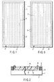
- FIG. 1 is a plan view showing the front surface, which is irradiated with the solar light, of a solar cell module according to the first embodiment of the present invention.
- a mark e.g., a two-dimensional code 3
- a peripheral region 2 on the front surface of a solar cell module 1.
- a semiconductor layer and a reverse electrode layer are formed successively on the reverse surface of the solar cell module 1, followed by coating the reverse electrode layer with a resin. Therefore, if the two-dimensional code 3 is put on the reverse surface of the solar cell module 1, it is difficult to read the two-dimensional code 3 and, thus, the code 3 is put on that region of the front surface which is irradiated with the solar light.
- the peripheral region 2 is a region positioned outside a plurality of separating grooves 5, i.e., generally 4 separating grooves, though two separating grooves are shown in the drawing.
- the peripheral region 2 is electrically separated from a power generating region 4 by the separating grooves 5.
- the peripheral region 2 has a width of 5 mm as measured from the periphery of the solar cell module 1.
- the peripheral region 2 in which the two-dimensional code 3 is put does not contribute to the power generation and, thus, does not affect the power generation. Also, the peripheral region 2 is not irradiated with a laser beam used for the laser scribing in the manufacturing process described below of the solar cell module 1.
- the two-dimensional code 3 is put in the region that is not irradiated with a laser beam. If the two-dimensional code 3 is irradiated with a laser beam, the two-dimensional code is damaged, resulting in failure to read the two-dimensional code 3. It follows that the control of the manufacturing process is adversely affected. It should also be noted that the laser beam is intercepted by the two-dimensional code 3, with the result that the laser scribing is adversely affected.
- the laser scribing is performed in the scribing step of the transparent electrode layer, the scribing step of the semiconductor layer, the scribing step of the reverse electrode layer, and in the scribing step for separating the power generation region from the peripheral region.
- a washing step using a detergent it is possible for a washing step using a detergent to be performed.
- the two-dimensional code 3 is used for controlling the subsequent manufacturing process. Therefore, the two-dimensional code 3 is put to the glass substrate before the glass substrate is subjected to the manufacturing process, or to the glass substrate in the stage of the initial manufacturing process, e.g., the glass substrate on which the transparent electrode layer is formed.
- the glass substrate having the two-dimensional code 3 put thereon is used in the various subsequent steps including, for example, the step of forming a transparent electrode layer and scribing the transparent electrode layer thus formed, the step of forming a semiconductor layer and scribing the semiconductor layer thus formed, the step of forming a reverse electrode layer and scribing the reverse electrode layer thus formed, the scribing step for separating the power generation region from the peripheral region, the encapsulating and the inspecting step.
- An apparatus for reading the two-dimensional code is arranged for some or all of these steps. As a result, the two-dimensional code 3 put to the glass substrate is read by the apparatus for reading the two-dimensional code, thereby controlling each manufacturing step.
- a film of a transparent metal oxide having an electrical conductivity such as tin oxide (SnO 2 ), indium tin oxide (ITO) or zinc oxide (ZnO) is formed on a transparent substrate 1 such as a glass substrate.
- the two-dimensional code 3 is put by a predetermined method, e.g., by using a metal transfer marker, to a predetermined position on the surface of the glass substrate 1 before formation of the metal oxide film or to a predetermined position on the surface of the glass substrate 1 after formation of the metal oxide film.
- the two-dimensional code 3 is read by a predetermined method so as to control the subsequent process. It is possible for the two-dimensional code 3 to represent, for example, the substrate number.
- the metal oxide film formed on the substrate is subjected to a laser-scribing so as to form on substantially the entire surface of the substrate a plurality of strip-like first electrode layers 12 extending in one direction of the substrate and separated from each other by a separating band interposed between the adjacent strips of the first electrode layer 12.
- a p-type hydrogenated amorphous silicon carbide layer p-type a-SiC:H
- an i-type hydrogenated amorphous silicon layer i-type a-Si:H
- an n-type hydrogenated amorphous silicon layer n-type a-Si:H
- the semiconductor layer is partly removed by a laser scribing to form an opening portion for an electric connection.
- a single semiconductor layer 13 is constructed to bridge two adjacent first electrode layers 12.
- a two dimensional code reader is arranged to permit the two dimensional code put to the passing substrate to be read by the reader.
- the information on the processing series and the processing data and time are added to the server.
- a second electrode layer 14 made of a metal such as aluminum (Al) or silver (Ag) is formed on the plural semiconductor layer regions 13. Further, a separating groove is formed by removing at least partly the second electrode layer by laser scribing along the opening for the electric connection.
- the second electrode layer and the semiconductor layer in the lead-out electrode portion in the vicinity of the connection terminal are removed by laser scribing. Also, the second electrode layer, the semiconductor layer and the first electrode layer on the outside thereof are removed by laser scribing to form a plurality of separating grooves 5 for separating the power generating region from the peripheral region.
- a two-dimensional code reader is also arranged after the laser scribing step to permit the two-dimensional code put to the passing substrate to be read by the reader. Also, the information on the processing series and the processing date and time are added to the server.
- a conductor 15 such as a solder-plated copper foil is mounted to the lead-out electrode portion of the first electrode by a bonding material such as an ultrasonic solder or an adhesive such as a conductive resin so as to permit the first electrode layer 12 to be electrically connected to the conductor 15.
- the conductor 15 functions as a lead-out electrode.
- Manufacture of a solar cell is finished by mounting the lead-out electrode, though it is possible for the solar cell to be coated with, for example, an encapsulant resin, and a frame member is mounted around the substrate, as required.
- the I-V characteristics and the insulation resistance of the solar cell thus prepared are measured so as to inspect whether or not the solar cell exhibits desired characteristics.
- the two-dimensional code put to the substrate is read, and the information on the measured values are recorded together with the information on the substrate and the information of each manufacturing step so as to control consistently the manufacturing process and the product quality.
- the history of the product can be known easily, and it is possible to clarify the cause of the failure for the measured value to fall within the predetermined range.
- a fine mark is simply put to a predetermined position on the surface of a transparent substrate, thereby making it possible to control all the subsequent manufacturing process and the product quality by simply reading the mark in the subsequent process. It follows that the control of the manufacturing process and the product quality, which are absolutely necessary in the mass production of photoelectric conversion apparatuses of various specifications, can be performed easily and promptly without using a costly facility.
- the front surface or reverse surface of the substrate can be known easily on the basis of the presence or absence of the mark.
- FIG. 3 is a plan view showing the front surface, which is irradiated with the solar light, of a solar cell module 1 according to the second embodiment of the present invention.
- a first mark e.g., a two-dimensional code 3 is put on the peripheral region 2 on the front surface of the solar cell module 1, as in the first embodiment.
- a semiconductor layer and a reverse electrode layer are formed successively on the back surface of the solar cell module 1, followed by coating the reverse electrode layer with a resin. Therefore, if the two-dimensional code 3 is put on the reverse surface of the solar cell module 1, it is difficult to read the two-dimensional code 3 and, thus, the code 3 is put on that region of the front surface which is irradiated with the solar light.
- the peripheral region 2 is a region positioned outside a plurality of separating grooves 5, i.e., generally 4 separating grooves, though two separating grooves are shown in the drawing.
- the peripheral region 2 is electrically separated from a power generating region 4 by the separating grooves 5.
- the peripheral region 2 has a width of 5 mm as measured from the periphery of the solar cell module 1.
- the peripheral region 2 in which the two-dimensional code 3 is put does not contribute to the power generation and, thus, does not affect the power generation. Also, the peripheral region 2 is not irradiated with a laser beam used for the laser scribing in the manufacturing process described below of the solar cell module 1.
- the two-dimensional code 3 is put in the region that is not irradiated with a laser beam. If the two-dimensional code 3 is irradiated with a laser beam, the two-dimensional code is damaged, resulting in failure to read the two-dimensional code 3. It follows that the control of the manufacturing process is adversely affected. It should also be noted that the laser beam is intercepted by the two-dimensional code 3, with the result that the laser scribing is adversely affected. Incidentally, in the case of using a mark that is not damaged by the irradiation with a laser beam, it is possible to put the first mark in the region irradiated with the laser beam in the laser scribing step during manufacture of the solar cell module 1.
- the laser scribing is performed in the scribing step of the transparent electrode layer, the scribing step of the semiconductor layer, the scribing step of the reverse electrode layer, and in the scribing step for separating the power generation region from the peripheral region.
- a washing step using a detergent it is possible for a washing step using a detergent to be performed.
- the two-dimensional code 3 is used for controlling the subsequent manufacturing process. Therefore, the two-dimensional code 3 is put to the glass substrate before the glass substrate is subjected to the manufacturing process, or to the glass substrate in the stage of the initial manufacturing process, e.g., the glass substrate on which the transparent electrode layer is formed.
- the glass substrate having the two-dimensional code 3 put thereon is used in the various subsequent steps including, for example, the step of forming a transparent electrode layer and scribing the transparent electrode layer thus formed, the step of forming a semiconductor layer and scribing the semiconductor layer thus formed, the step of forming a reverse electrode layer and scribing the reverse electrode layer thus formed, the scribing step for separating the power generation region from the peripheral region, and the step for mounting a lead.
- An apparatus for reading the two-dimensional code is arranged for some or all of these steps. As a result, the two-dimensional code 3 put to the glass substrate is read by the apparatus for reading the two-dimensional code, thereby controlling each manufacturing step.
- the information read by the reading apparatus is put to the reverse surface of the substrate as a second mark 21 in the form of a bar code or a character printed on, for example, a bar code label.
- the information of the second mark 21 is printed again on a bar code label and, then, the label is attached to the reverse surface of the substrate for transfer to the subsequent step.
- a label having the product number printed thereon is attached to the reverse surface of the substrate to obtain the final product and, then, the final product is stored in a warehouse.
- the second mark 21 can be put to the substrate by simply attaching a label having, for example, a bar code printed thereon to the reverse surface of the substrate and, thus, can be a cheap mark, compared with the first mark, e.g., a two-dimensional mark that is printed directly on the surface of the substrate.
- the second mark does not necessitate a costly reading apparatus that is required in the case of using a two-dimensional mark.
- the second mark can be made larger in size than the first mark and, thus, is excellent in visibility.
- two kinds of marks are used optionally depending on the stages of the manufacturing process so as to control with a computer the information owned by these marks and the information such as the processing date and time of each step, the number of the series of the products, the measured data and the rank (judgment). It follows that the manufacturing process of the solar cell and the quality of the product can be controlled consistently and efficiently.
- a film of a transparent metal oxide having an electrical conductivity such as tin oxide (SnO 2 ), indium tin oxide (ITO) or zinc oxide (ZnO) is formed on a transparent substrate 1 such as a glass substrate.
- the two-dimensional code 3 is put by a predetermined method, e.g., by using a metal transfer marker, to a predetermined position on the surface of the glass substrate 1 before formation of the metal oxide film or to a predetermined position on the surface of the glass substrate 1 after formation of the metal oxide film. It is possible for the two-dimensional code 3 to contain various information such as the manufactures and kind of the substrate and the substrate lot number in addition to the substrate number.
- the two-dimensional code 3 is read by a predetermined method so as to control the subsequent process.
- the metal oxide film formed on the substrate is subjected to a laser-scribing so as to form on substantially the entire surface of the substrate a plurality of strip-like first electrode layers 12 extending in one direction of the substrate and separated from each other by a separating band interposed between the adjacent strips of the first electrode layer 12.
- a p-type hydrogenated amorphous silicon carbide layer p-type a-SiC:H
- an i-type hydrogenated amorphous silicon layer i-type a-Si:H
- an n-type hydrogenated amorphous silicon layer n-type a-Si:H
- the semiconductor layer is partly removed by a laser scribing to form an opening portion for an electric connection.
- a single region of the semiconductor layer 13 is constructed to bridge two adjacent first electrode layers 12.
- a two dimensional code reader is arranged to permit the two dimensional code put to the passing substrate to be read by the reader.
- the information on the processing series and the processing data and time are added to the server.
- a second electrode layer 14 made of a metal such as aluminum (Al) or silver (Ag) is formed on the plural semiconductor layer regions 13. Further, a separating groove is formed by removing at least partly the second electrode layer by laser scribing along the opening for the electric connection.
- the second electrode layer and the semiconductor layer in the lead-out electrode portion in the vicinity of the connection terminal are removed by laser scribing. Also, the second electrode layer, the semiconductor layer and the first electrode layer on the outside thereof are removed by laser scribing to form a plurality of separating grooves 5 for separating the power generating region from the peripheral region.
- a two-dimensional code reader is also arranged after the laser scribing step to permit the two-dimensional code put to the passing substrate to be read by the reader. Also, the information on the processing series and the processing date and time are added to the server.
- a conductor 15 such as a solder-plated copper foil is mounted to the lead-out electrode portion of the first electrode by a bonding material such as an ultrasonic solder or an adhesive such as a conductive resin so as to permit the first electrode layer 12 to be electrically connected to the conductor 15.
- a bonding material such as an ultrasonic solder or an adhesive such as a conductive resin
- a two-dimensional code reader is arranged to permit the two-dimensional code put to the passing substrate to be read by the two-dimensional code reader.
- the substrate number that has been read is printed on a bar code label 21 in the form of a bar code or a character together with the abbreviated symbol of the kind and rank of the substrate. After the printing, the bar code label 21 is attached to an edge portion on the reverse surface of the substrate, as shown in FIG. 3.
- the solar cell is sealed by coating, for example, an encapsulant resin.
- the I-V characteristics and the insulation resistance of the solar cell are measured to inspect whether or not the solar cell exhibits desired characteristics.
- the bar code is read from the bar code label 21, and the measured data are added to the server.
- the product number is printed in the form of a character on a label, and the label is attached to an edge portion on the reverse surface of the substrate so as to finish manufacture of the solar cell module.
- the solar cell module thus manufactured is stored in a warehouse.
- the manufacturing process before the encapsulating is controlled by a mark put in an edge portion on the front surface of the substrate and excellent in resistance to the subsequent process, e.g., a two-dimensional code.
- the manufacturing process after the encapsulating is controlled by a mark put in an edge portion on the reverse surface of the substrate, which is cheap and excellent in visibility.
- the mark consists of, for example, a bar code.
- the information contained in these two kinds of marks and read out in each step is processed together with the information input in each step, making it possible to control consistently the manufacturing process and the product quality of the photoelectric conversion apparatus.
- two kinds of marks are used optionally depending on the stages of the manufacturing process so as to control with a computer the information owned by these marks and the information such as the processing date and time of each step, the number of the series of the products, the measured data and the rank (judgment). It follows that the manufacturing process of the solar cell and the quality of the product can be controlled consistently and efficiently.
Landscapes
- Photovoltaic Devices (AREA)
- Light Receiving Elements (AREA)
Abstract
Description
Claims (15)
- A method of controlling the manufacturing process of a photoelectric conversion apparatus, said manufacturing process comprising the steps of successively forming a transparent electrode layer, a semiconductor layer and a reverse electrode layer in a laminated fashion on one surface of a transparent substrate, laser-scribing each of these layers as formed to form a plurality of solar cells, electrically connecting these solar cells to form a solar cell module, laser-scribing the peripheral portion of the transparent substrate of the solar cell module to electrically separate the power generation region of the solar cell module from the peripheral region to obtain a photoelectric conversion apparatus, and inspecting the resultant photoelectric conversion apparatus, wherein said controlling method comprises the step of putting a mark (3) for controlling the manufacturing process in a peripheral region (2) on an another surface of said transparent substrate or in that region of a side surface of the transparent substrate, which is not irradiated with the laser beam used for the laser-scribing of each of the transparent electrode layer, the semiconductor layer and the reverse electrode layer, said mark (3) being read in the subsequent process and the subsequent process being controlled by utilizing the mark thus read.
- The method according to claim 1, characterized in that said mark is put in a peripheral region (2) of said transparent substrate, said peripheral region (2) having a width of 5 mm as measured from the periphery of the transparent substrate.
- The method according to claim 1 or 2, characterized in that said mark (3) consists of a bar code or a two-dimensional mark.
- The method according to claim 1, 2 or 3, characterized in that said mark (3) is formed by laser carving.
- The method according to claim 1, 2 or 3, characterized in that said mark (3) is formed by printing.
- The method according to any of claims 1 to 5, characterized in that said mark (3) is at least one kind selected from the group consisting of a two-dimensional code, a bar code, a character, and a numeral formed by direct printing on the surface of the substrate.
- The method according to any of claims 1 to 6, characterized in that said mark (3) is read for controlling each of the subsequent manufacturing steps and, then, another mark (21) is put on the transparent substrate for controlling the subsequent steps by utilizing said another mark (21).
- The method according to claim 7, characterized in that said mark (3) has resistance to the subsequent steps.
- The method according to claim 7 or 8, characterized in that said another mark (21) is excellent in visibility.
- The method according to claim 7, 8 or 9, characterized in that said another mark (21) is at least one kind selected from the group consisting of a bar code, a character and a numeral that are printed on a label attached to the back surface of the substrate.
- A quality controlling system using a mark, comprising:means for putting a first mark (3) on a surface of a transparent substrate in the process of manufacturing a photoelectric conversion apparatus;means controlling the subsequent step by utilizing the first mark put on the transparent substrate;means for putting a second mark (21) on the transparent substrate; andmeans for controlling the subsequent step by utilizing the second mark (21) put on the transparent substrate.
- The quality controlling method according to claim 11, characterized in that said first mark (3) has resistance to the subsequent step.
- The quality controlling method according to claim 11 or 12, characterized in that said first mark (3) is at least one kind selected from the group consisting of a two-dimensional code, a bar code, a character, and a numeral, which are formed by direct printing on the front surface of the substrate.
- The quality controlling method according to claim 11, 12 or 13, characterized in that said second mark (21) is excellent in visibility.
- The quality controlling method according to claim 14, characterized in that said second mark (21) is at least one kind selected from the group consisting of a bar code, a character, and a numeral, which are printed on a label attached to the reverse surface of the substrate.
Priority Applications (1)
| Application Number | Priority Date | Filing Date | Title |
|---|---|---|---|
| EP07112029A EP1868249B1 (en) | 1999-09-28 | 2000-03-06 | Method of controlling manufacturing process of photoelectric conversion apparatus |
Applications Claiming Priority (4)
| Application Number | Priority Date | Filing Date | Title |
|---|---|---|---|
| JP27490799A JP2001102604A (en) | 1999-09-28 | 1999-09-28 | Manufacturing process management method for photoelectric conversion device |
| JP27490799 | 1999-09-28 | ||
| JP28566499A JP4414521B2 (en) | 1999-10-06 | 1999-10-06 | Photoelectric conversion device and quality control system for photoelectric conversion device |
| JP28566499 | 1999-10-06 |
Related Child Applications (3)
| Application Number | Title | Priority Date | Filing Date |
|---|---|---|---|
| EP07112029A Division EP1868249B1 (en) | 1999-09-28 | 2000-03-06 | Method of controlling manufacturing process of photoelectric conversion apparatus |
| EP07112029.9 Division-Into | 2007-07-09 | ||
| EP10157194.1 Division-Into | 2010-03-22 |
Publications (3)
| Publication Number | Publication Date |
|---|---|
| EP1089346A2 true EP1089346A2 (en) | 2001-04-04 |
| EP1089346A3 EP1089346A3 (en) | 2006-05-17 |
| EP1089346B1 EP1089346B1 (en) | 2011-03-02 |
Family
ID=26551246
Family Applications (2)
| Application Number | Title | Priority Date | Filing Date |
|---|---|---|---|
| EP07112029A Expired - Lifetime EP1868249B1 (en) | 1999-09-28 | 2000-03-06 | Method of controlling manufacturing process of photoelectric conversion apparatus |
| EP00104449A Expired - Lifetime EP1089346B1 (en) | 1999-09-28 | 2000-03-06 | Method of controlling manufacturing process of photoelectric conversion apparatus |
Family Applications Before (1)
| Application Number | Title | Priority Date | Filing Date |
|---|---|---|---|
| EP07112029A Expired - Lifetime EP1868249B1 (en) | 1999-09-28 | 2000-03-06 | Method of controlling manufacturing process of photoelectric conversion apparatus |
Country Status (6)
| Country | Link |
|---|---|
| US (1) | US6578764B1 (en) |
| EP (2) | EP1868249B1 (en) |
| AT (2) | ATE500615T1 (en) |
| AU (1) | AU776867C (en) |
| DE (1) | DE60045678D1 (en) |
| ES (1) | ES2360031T3 (en) |
Cited By (5)
| Publication number | Priority date | Publication date | Assignee | Title |
|---|---|---|---|---|
| WO2002064854A1 (en) * | 2001-02-15 | 2002-08-22 | Kaneka Corporation | Method of forming silicon thin film and silicon thin film solar cell |
| WO2007099138A1 (en) | 2006-02-28 | 2007-09-07 | Q-Cells Ag | Solar cell marking method, and solar cell |
| DE102007032283A1 (en) * | 2007-07-11 | 2009-01-15 | Stein, Wilhelm, Dr. | Thin-film solar cell module and method for its production |
| DE102008043750A1 (en) * | 2008-11-14 | 2010-05-20 | Q-Cells Se | Process for the marking / coding of a solar cell and solar cell |
| EP2249395A4 (en) * | 2008-02-27 | 2013-01-16 | Sharp Kk | THIN FILM SOLAR CELL AND METHOD OF MANUFACTURING THE SAME |
Families Citing this family (22)
| Publication number | Priority date | Publication date | Assignee | Title |
|---|---|---|---|---|
| TWI342459B (en) * | 2004-03-26 | 2011-05-21 | Chimei Innolux Corp | Glass substrate |
| CN100377074C (en) * | 2004-03-27 | 2008-03-26 | 鸿富锦精密工业(深圳)有限公司 | Glass base board |
| KR101301664B1 (en) * | 2007-08-06 | 2013-08-29 | 주성엔지니어링(주) | The method for manufacturing Thin film type Solar Cell, and Thin film type Solar Cell made by the method |
| JP2010538476A (en) * | 2007-08-31 | 2010-12-09 | アプライド マテリアルズ インコーポレイテッド | Photovoltaic production line |
| US20100047954A1 (en) * | 2007-08-31 | 2010-02-25 | Su Tzay-Fa Jeff | Photovoltaic production line |
| EP3333280B1 (en) | 2007-09-12 | 2026-04-01 | Flisom AG | Method for manufacturing a compound film with compositional grading |
| US20090188603A1 (en) * | 2008-01-25 | 2009-07-30 | Applied Materials, Inc. | Method and apparatus for controlling laminator temperature on a solar cell |
| US7981778B2 (en) * | 2009-07-22 | 2011-07-19 | Applied Materials, Inc. | Directional solid phase crystallization of thin amorphous silicon for solar cell applications |
| WO2010027712A2 (en) * | 2008-08-26 | 2010-03-11 | Applied Materials, Inc. | Laser material removal methods and apparatus |
| KR101520044B1 (en) * | 2009-01-30 | 2015-05-14 | 삼성에스디아이 주식회사 | Solar cell module and method for manufacturing the same |
| WO2010091025A2 (en) * | 2009-02-04 | 2010-08-12 | Applied Materials, Inc. | Metrology and inspection suite for a solar production line |
| US20100330711A1 (en) * | 2009-06-26 | 2010-12-30 | Applied Materials, Inc. | Method and apparatus for inspecting scribes in solar modules |
| US20110008947A1 (en) * | 2009-07-13 | 2011-01-13 | Applied Materials, Inc. | Apparatus and method for performing multifunction laser processes |
| US20110005458A1 (en) * | 2009-07-13 | 2011-01-13 | Applied Materials, Inc. | Method and apparatus for improving scribe accuracy in solar cell modules |
| US20110065227A1 (en) * | 2009-09-15 | 2011-03-17 | Applied Materials, Inc. | Common laser module for a photovoltaic production line |
| DE102010060908A1 (en) * | 2010-11-30 | 2012-05-31 | Q-Cells Se | Method for marking semiconductor wafer used in manufacturing process of solar cell, involves printing information including process parameters in edge of wafer |
| CN103000752A (en) * | 2011-09-19 | 2013-03-27 | 无锡尚德太阳能电力有限公司 | Thin-film solar cell scribing machine and method |
| NL2014040B1 (en) * | 2014-12-23 | 2016-10-12 | Stichting Energieonderzoek Centrum Nederland | Method of making a curent collecting grid for solar cells. |
| US10923606B2 (en) * | 2016-10-26 | 2021-02-16 | Kaneka Corporation | Photoelectric conversion element |
| CN113439075A (en) | 2019-02-13 | 2021-09-24 | 日本碍子株式会社 | Manufacturing method of ceramic part, ceramic molded body, and manufacturing system of ceramic part |
| DE102019006090A1 (en) * | 2019-08-29 | 2021-03-04 | Azur Space Solar Power Gmbh | Marking process |
| JP7815036B2 (en) * | 2022-06-03 | 2026-02-17 | キオクシア株式会社 | Semiconductor device and manufacturing method thereof |
Family Cites Families (17)
| Publication number | Priority date | Publication date | Assignee | Title |
|---|---|---|---|---|
| US3576540A (en) * | 1967-11-20 | 1971-04-27 | Sundstrand Corp | Plural machine tool and part handling control system |
| US4446362A (en) * | 1979-05-21 | 1984-05-01 | Rca Corporation | Workpiece with abraded machine-readable marking therein and method of making |
| US4327283A (en) * | 1979-09-24 | 1982-04-27 | Rca Corporation | Workpiece with machine-readable marking recessed therein and method of making same |
| JPS603164A (en) * | 1983-06-21 | 1985-01-09 | Sanyo Electric Co Ltd | Method of manufacturing photovoltaic device |
| US4510673A (en) * | 1983-06-23 | 1985-04-16 | International Business Machines Corporation | Laser written chip identification method |
| JPS61263172A (en) * | 1985-05-16 | 1986-11-21 | Fuji Electric Co Ltd | Method for manufacturing thin film solar cells |
| CA2011296A1 (en) * | 1989-05-15 | 1990-11-15 | Douglas C. Bossen | Presence/absence bar code |
| JPH0437085A (en) * | 1990-06-01 | 1992-02-07 | Hitachi Ltd | Printed wiring board and its manufacturing method |
| JPH0451156A (en) | 1990-06-19 | 1992-02-19 | Canon Inc | Heat fixing method and toner |
| US5501744A (en) * | 1992-01-13 | 1996-03-26 | Photon Energy, Inc. | Photovoltaic cell having a p-type polycrystalline layer with large crystals |
| IT1272036B (en) * | 1993-11-05 | 1997-06-11 | Marelli Autronica | REGISTRATION SYSTEM FOR A PRODUCTION LINE. |
| JP2867904B2 (en) | 1994-12-26 | 1999-03-10 | 株式会社デンソー | 2D code reader |
| JP3188158B2 (en) * | 1995-09-01 | 2001-07-16 | シャープ株式会社 | Management system for transparent body processing |
| JPH09278494A (en) * | 1996-04-15 | 1997-10-28 | Corning Japan Kk | Method for marking glass substrate |
| DE69704698T2 (en) * | 1996-12-27 | 2002-01-31 | Miyachi Technos Corp., Noda | Method of labeling an object that uses a laser beam |
| JP3915851B2 (en) | 1996-12-27 | 2007-05-16 | オムロン株式会社 | Method for marking using a laser beam and method for marking identification information on a glass substrate in the manufacturing process of a display panel |
| JP3805889B2 (en) * | 1997-06-20 | 2006-08-09 | 株式会社カネカ | Solar cell module and manufacturing method thereof |
-
2000
- 2000-03-06 ES ES00104449T patent/ES2360031T3/en not_active Expired - Lifetime
- 2000-03-06 AT AT00104449T patent/ATE500615T1/en not_active IP Right Cessation
- 2000-03-06 AT AT07112029T patent/ATE516598T1/en not_active IP Right Cessation
- 2000-03-06 EP EP07112029A patent/EP1868249B1/en not_active Expired - Lifetime
- 2000-03-06 EP EP00104449A patent/EP1089346B1/en not_active Expired - Lifetime
- 2000-03-06 DE DE60045678T patent/DE60045678D1/en not_active Expired - Lifetime
- 2000-03-07 US US09/521,193 patent/US6578764B1/en not_active Expired - Lifetime
- 2000-03-08 AU AU20725/00A patent/AU776867C/en not_active Expired
Cited By (11)
| Publication number | Priority date | Publication date | Assignee | Title |
|---|---|---|---|---|
| WO2002064854A1 (en) * | 2001-02-15 | 2002-08-22 | Kaneka Corporation | Method of forming silicon thin film and silicon thin film solar cell |
| US6849560B2 (en) | 2001-02-15 | 2005-02-01 | Kaneka Corporation | Method of depositing silicon thin film and silicon thin film solar cell |
| AU2002232197B2 (en) * | 2001-02-15 | 2005-12-15 | Kaneka Corporation | Method of forming silicon thin film and silicon thin film solar cell |
| AU2002232197C1 (en) * | 2001-02-15 | 2006-11-09 | Kaneka Corporation | Method of forming silicon thin film and silicon thin film solar cell |
| WO2007099138A1 (en) | 2006-02-28 | 2007-09-07 | Q-Cells Ag | Solar cell marking method, and solar cell |
| US8492240B2 (en) | 2006-02-28 | 2013-07-23 | Hanwha Q.CELLS GmbH | Solar-cell marking method and solar cell |
| DE102007032283A1 (en) * | 2007-07-11 | 2009-01-15 | Stein, Wilhelm, Dr. | Thin-film solar cell module and method for its production |
| US8470615B2 (en) | 2007-07-11 | 2013-06-25 | Wilhelm Stein | Thin layer solar cell module and method for producing it |
| US8846419B2 (en) | 2007-07-11 | 2014-09-30 | Wilhelm Stein | Thin layer solar cell module and method for producing it |
| EP2249395A4 (en) * | 2008-02-27 | 2013-01-16 | Sharp Kk | THIN FILM SOLAR CELL AND METHOD OF MANUFACTURING THE SAME |
| DE102008043750A1 (en) * | 2008-11-14 | 2010-05-20 | Q-Cells Se | Process for the marking / coding of a solar cell and solar cell |
Also Published As
| Publication number | Publication date |
|---|---|
| EP1089346A3 (en) | 2006-05-17 |
| ES2360031T3 (en) | 2011-05-31 |
| EP1868249A2 (en) | 2007-12-19 |
| ATE516598T1 (en) | 2011-07-15 |
| AU2072500A (en) | 2001-03-29 |
| AU776867C (en) | 2005-06-16 |
| US6578764B1 (en) | 2003-06-17 |
| EP1868249B1 (en) | 2011-07-13 |
| DE60045678D1 (en) | 2011-04-14 |
| EP1089346B1 (en) | 2011-03-02 |
| EP1868249A3 (en) | 2008-11-12 |
| AU776867B2 (en) | 2004-09-23 |
| ATE500615T1 (en) | 2011-03-15 |
Similar Documents
| Publication | Publication Date | Title |
|---|---|---|
| EP1868249B1 (en) | Method of controlling manufacturing process of photoelectric conversion apparatus | |
| US5296043A (en) | Multi-cells integrated solar cell module and process for producing the same | |
| EP2302692B1 (en) | Solar battery module and method for manufacturing the same | |
| EP0542961B1 (en) | Improved solar cell and method of making same | |
| CN101515609B (en) | Thin film type solar cell and method for manufacturing the same | |
| EP0153041A2 (en) | Improved large area photovoltaic cell and method for producing same | |
| US20090032109A1 (en) | Cis based thin-film photovoltaic module and process for producing the same | |
| WO2012037191A2 (en) | Improved photovoltaic cell assembly and method | |
| JP5655236B2 (en) | Method for producing photovoltaic module comprising a plurality of semiconductor cells each contacted on the rear side | |
| US20150129011A1 (en) | Solar cell module | |
| JP2012104512A (en) | Thin film solar cell module and method of manufacturing the same | |
| US20160064575A1 (en) | Back-contact back-sheet for photovoltaic modules with pass-through electric contacts | |
| JP2001102604A (en) | Manufacturing process management method for photoelectric conversion device | |
| EP2879191A1 (en) | Method for manufacturing thin-film solar battery module | |
| JP4414521B2 (en) | Photoelectric conversion device and quality control system for photoelectric conversion device | |
| JP2008113053A (en) | Method for controlling manufacturing process of photoelectric conversion device | |
| US20120240980A1 (en) | Interconnection Schemes for Photovoltaic Cells | |
| WO2011103332A2 (en) | Methods of forming photovoltaic modules | |
| US9076900B2 (en) | Solar cell module and solar cell | |
| JP2009260399A (en) | Quality management system using mark | |
| JP2008113054A (en) | Quality control system for photoelectric conversion device | |
| US20110023933A1 (en) | Interconnection Schemes for Photovoltaic Cells | |
| US20250160038A1 (en) | Solar cell fabrication | |
| WO2012039332A1 (en) | Bypass diode device, method for inspecting same, and method for manufacturing film diode device | |
| US20120049310A1 (en) | Thin film photoelectric conversion module and fabrication method of the same |
Legal Events
| Date | Code | Title | Description |
|---|---|---|---|
| PUAI | Public reference made under article 153(3) epc to a published international application that has entered the european phase |
Free format text: ORIGINAL CODE: 0009012 |
|
| AK | Designated contracting states |
Kind code of ref document: A2 Designated state(s): AT BE CH CY DE DK ES FI FR GB GR IE IT LI LU MC NL PT SE |
|
| AX | Request for extension of the european patent |
Free format text: AL;LT;LV;MK;RO;SI |
|
| PUAL | Search report despatched |
Free format text: ORIGINAL CODE: 0009013 |
|
| AK | Designated contracting states |
Kind code of ref document: A3 Designated state(s): AT BE CH CY DE DK ES FI FR GB GR IE IT LI LU MC NL PT SE |
|
| AX | Request for extension of the european patent |
Extension state: AL LT LV MK RO SI |
|
| 17P | Request for examination filed |
Effective date: 20060720 |
|
| 17Q | First examination report despatched |
Effective date: 20061228 |
|
| AKX | Designation fees paid |
Designated state(s): AT BE CH CY DE DK ES FI FR GB GR IE IT LI LU MC NL PT SE |
|
| GRAP | Despatch of communication of intention to grant a patent |
Free format text: ORIGINAL CODE: EPIDOSNIGR1 |
|
| RIC1 | Information provided on ipc code assigned before grant |
Ipc: H01L 27/142 20060101AFI20100517BHEP |
|
| GRAS | Grant fee paid |
Free format text: ORIGINAL CODE: EPIDOSNIGR3 |
|
| GRAA | (expected) grant |
Free format text: ORIGINAL CODE: 0009210 |
|
| AK | Designated contracting states |
Kind code of ref document: B1 Designated state(s): AT BE CH CY DE DK ES FI FR GB GR IE IT LI LU MC NL PT SE |
|
| REG | Reference to a national code |
Ref country code: GB Ref legal event code: FG4D |
|
| REG | Reference to a national code |
Ref country code: CH Ref legal event code: EP |
|
| REG | Reference to a national code |
Ref country code: IE Ref legal event code: FG4D |
|
| REF | Corresponds to: |
Ref document number: 60045678 Country of ref document: DE Date of ref document: 20110414 Kind code of ref document: P |
|
| REG | Reference to a national code |
Ref country code: DE Ref legal event code: R096 Ref document number: 60045678 Country of ref document: DE Effective date: 20110414 |
|
| REG | Reference to a national code |
Ref country code: ES Ref legal event code: FG2A Ref document number: 2360031 Country of ref document: ES Kind code of ref document: T3 Effective date: 20110531 |
|
| REG | Reference to a national code |
Ref country code: NL Ref legal event code: VDEP Effective date: 20110302 |
|
| REG | Reference to a national code |
Ref country code: GR Ref legal event code: EP Ref document number: 20110401193 Country of ref document: GR Effective date: 20110614 |
|
| PG25 | Lapsed in a contracting state [announced via postgrant information from national office to epo] |
Ref country code: SE Free format text: LAPSE BECAUSE OF FAILURE TO SUBMIT A TRANSLATION OF THE DESCRIPTION OR TO PAY THE FEE WITHIN THE PRESCRIBED TIME-LIMIT Effective date: 20110302 |
|
| PG25 | Lapsed in a contracting state [announced via postgrant information from national office to epo] |
Ref country code: AT Free format text: LAPSE BECAUSE OF FAILURE TO SUBMIT A TRANSLATION OF THE DESCRIPTION OR TO PAY THE FEE WITHIN THE PRESCRIBED TIME-LIMIT Effective date: 20110302 Ref country code: CY Free format text: LAPSE BECAUSE OF FAILURE TO SUBMIT A TRANSLATION OF THE DESCRIPTION OR TO PAY THE FEE WITHIN THE PRESCRIBED TIME-LIMIT Effective date: 20110302 Ref country code: FI Free format text: LAPSE BECAUSE OF FAILURE TO SUBMIT A TRANSLATION OF THE DESCRIPTION OR TO PAY THE FEE WITHIN THE PRESCRIBED TIME-LIMIT Effective date: 20110302 Ref country code: NL Free format text: LAPSE BECAUSE OF FAILURE TO SUBMIT A TRANSLATION OF THE DESCRIPTION OR TO PAY THE FEE WITHIN THE PRESCRIBED TIME-LIMIT Effective date: 20110302 |
|
| PG25 | Lapsed in a contracting state [announced via postgrant information from national office to epo] |
Ref country code: BE Free format text: LAPSE BECAUSE OF FAILURE TO SUBMIT A TRANSLATION OF THE DESCRIPTION OR TO PAY THE FEE WITHIN THE PRESCRIBED TIME-LIMIT Effective date: 20110302 |
|
| PG25 | Lapsed in a contracting state [announced via postgrant information from national office to epo] |
Ref country code: PT Free format text: LAPSE BECAUSE OF FAILURE TO SUBMIT A TRANSLATION OF THE DESCRIPTION OR TO PAY THE FEE WITHIN THE PRESCRIBED TIME-LIMIT Effective date: 20110704 Ref country code: MC Free format text: LAPSE BECAUSE OF NON-PAYMENT OF DUE FEES Effective date: 20110331 |
|
| REG | Reference to a national code |
Ref country code: CH Ref legal event code: PL |
|
| REG | Reference to a national code |
Ref country code: IE Ref legal event code: MM4A |
|
| PLBE | No opposition filed within time limit |
Free format text: ORIGINAL CODE: 0009261 |
|
| STAA | Information on the status of an ep patent application or granted ep patent |
Free format text: STATUS: NO OPPOSITION FILED WITHIN TIME LIMIT |
|
| PG25 | Lapsed in a contracting state [announced via postgrant information from national office to epo] |
Ref country code: IE Free format text: LAPSE BECAUSE OF NON-PAYMENT OF DUE FEES Effective date: 20110306 Ref country code: CH Free format text: LAPSE BECAUSE OF NON-PAYMENT OF DUE FEES Effective date: 20110331 Ref country code: LI Free format text: LAPSE BECAUSE OF NON-PAYMENT OF DUE FEES Effective date: 20110331 |
|
| 26N | No opposition filed |
Effective date: 20111205 |
|
| PG25 | Lapsed in a contracting state [announced via postgrant information from national office to epo] |
Ref country code: DK Free format text: LAPSE BECAUSE OF FAILURE TO SUBMIT A TRANSLATION OF THE DESCRIPTION OR TO PAY THE FEE WITHIN THE PRESCRIBED TIME-LIMIT Effective date: 20110302 |
|
| REG | Reference to a national code |
Ref country code: DE Ref legal event code: R097 Ref document number: 60045678 Country of ref document: DE Effective date: 20111205 |
|
| REG | Reference to a national code |
Ref country code: FR Ref legal event code: CA Effective date: 20130416 |
|
| PG25 | Lapsed in a contracting state [announced via postgrant information from national office to epo] |
Ref country code: LU Free format text: LAPSE BECAUSE OF NON-PAYMENT OF DUE FEES Effective date: 20110306 |
|
| REG | Reference to a national code |
Ref country code: FR Ref legal event code: PLFP Year of fee payment: 16 |
|
| REG | Reference to a national code |
Ref country code: FR Ref legal event code: PLFP Year of fee payment: 17 |
|
| PGFP | Annual fee paid to national office [announced via postgrant information from national office to epo] |
Ref country code: GR Payment date: 20160212 Year of fee payment: 17 |
|
| REG | Reference to a national code |
Ref country code: FR Ref legal event code: PLFP Year of fee payment: 18 |
|
| PGFP | Annual fee paid to national office [announced via postgrant information from national office to epo] |
Ref country code: ES Payment date: 20170214 Year of fee payment: 18 Ref country code: IT Payment date: 20170320 Year of fee payment: 18 |
|
| REG | Reference to a national code |
Ref country code: FR Ref legal event code: PLFP Year of fee payment: 19 |
|
| PG25 | Lapsed in a contracting state [announced via postgrant information from national office to epo] |
Ref country code: GR Free format text: LAPSE BECAUSE OF NON-PAYMENT OF DUE FEES Effective date: 20171005 |
|
| PG25 | Lapsed in a contracting state [announced via postgrant information from national office to epo] |
Ref country code: IT Free format text: LAPSE BECAUSE OF NON-PAYMENT OF DUE FEES Effective date: 20180306 |
|
| PGFP | Annual fee paid to national office [announced via postgrant information from national office to epo] |
Ref country code: DE Payment date: 20190219 Year of fee payment: 20 Ref country code: GB Payment date: 20190306 Year of fee payment: 20 |
|
| PGFP | Annual fee paid to national office [announced via postgrant information from national office to epo] |
Ref country code: FR Payment date: 20190213 Year of fee payment: 20 |
|
| REG | Reference to a national code |
Ref country code: ES Ref legal event code: FD2A Effective date: 20190904 |
|
| PG25 | Lapsed in a contracting state [announced via postgrant information from national office to epo] |
Ref country code: ES Free format text: LAPSE BECAUSE OF NON-PAYMENT OF DUE FEES Effective date: 20180307 |
|
| REG | Reference to a national code |
Ref country code: DE Ref legal event code: R071 Ref document number: 60045678 Country of ref document: DE |
|
| REG | Reference to a national code |
Ref country code: GB Ref legal event code: PE20 Expiry date: 20200305 |
|
| PG25 | Lapsed in a contracting state [announced via postgrant information from national office to epo] |
Ref country code: GB Free format text: LAPSE BECAUSE OF EXPIRATION OF PROTECTION Effective date: 20200305 |