EP1094352A2 - Optical imaging head having a multiple writing beam source - Google Patents
Optical imaging head having a multiple writing beam source Download PDFInfo
- Publication number
- EP1094352A2 EP1094352A2 EP00203618A EP00203618A EP1094352A2 EP 1094352 A2 EP1094352 A2 EP 1094352A2 EP 00203618 A EP00203618 A EP 00203618A EP 00203618 A EP00203618 A EP 00203618A EP 1094352 A2 EP1094352 A2 EP 1094352A2
- Authority
- EP
- European Patent Office
- Prior art keywords
- image
- lens group
- radiation
- medium
- magnification
- Prior art date
- Legal status (The legal status is an assumption and is not a legal conclusion. Google has not performed a legal analysis and makes no representation as to the accuracy of the status listed.)
- Granted
Links
Images
Classifications
-
- G—PHYSICS
- G02—OPTICS
- G02B—OPTICAL ELEMENTS, SYSTEMS OR APPARATUS
- G02B26/00—Optical devices or arrangements for the control of light using movable or deformable optical elements
- G02B26/08—Optical devices or arrangements for the control of light using movable or deformable optical elements for controlling the direction of light
- G02B26/10—Scanning systems
- G02B26/106—Scanning systems having diffraction gratings as scanning elements, e.g. holographic scanners
-
- G—PHYSICS
- G02—OPTICS
- G02B—OPTICAL ELEMENTS, SYSTEMS OR APPARATUS
- G02B13/00—Optical objectives specially designed for the purposes specified below
- G02B13/02—Telephoto objectives, i.e. systems of the type + - in which the distance from the front vertex to the image plane is less than the equivalent focal length
-
- G—PHYSICS
- G02—OPTICS
- G02B—OPTICAL ELEMENTS, SYSTEMS OR APPARATUS
- G02B13/00—Optical objectives specially designed for the purposes specified below
- G02B13/22—Telecentric objectives or lens systems
-
- G—PHYSICS
- G02—OPTICS
- G02B—OPTICAL ELEMENTS, SYSTEMS OR APPARATUS
- G02B26/00—Optical devices or arrangements for the control of light using movable or deformable optical elements
- G02B26/08—Optical devices or arrangements for the control of light using movable or deformable optical elements for controlling the direction of light
- G02B26/0808—Optical devices or arrangements for the control of light using movable or deformable optical elements for controlling the direction of light by means of one or more diffracting elements
Definitions
- the invention relates generally to an improved optical imaging head for use in transferring images to a recording medium, and more particularly, to a dual telecentric, high powered optical imaging head operating with zero order diffractive radiation in an external drum imagesetter.
- a typical first step in the overall process is prepress operations, that is, to transform digital information representing the image of interest onto a light or thermal sensitive medium, e.g. a printing plate, which is then used to transfer the image any number of times on a printing press.
- prepress technologies have evolved, the time required to create the image has been reduced while the quality of the image has improved.
- media used for film, plates, proofing and final production This evolution continues to drive the requirement for a faster, higher quality, imaging system capable of imaging on many different recording media.
- One method for reducing imaging time is to increase the number of beams that write on the media at any one time.
- AOM multi-channel acousto-optical modulator
- DMDTM digital micromirror devices
- lanthanum modified lead zirconate titanate which can be fabricated as a transmissive ferroelectric ceramic modulator, also known as PLZTs.
- GLV multi-element modulator
- This GLV is an addressable diffraction grating, formed of moving parts on the surface of a silicon chip.
- Each GLV pixel consists of dual-supported parallel ribbons formed of silicon nitride and coated with a reflective aluminium top layer.
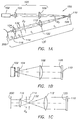
- Figure 1A is a side view optical diagram of a preferred embodiment
- an optical imaging head for transferring an image onto a medium could be designed that, when included in an imaging system, made it possible to image faster and with higher efficiency than the prior art devices.
- Such an imaging head includes a line illumination module for generating a substantially uniform line of radiation; a grating light valve which receives the line of radiation and generates diffractive orders of modulated radiation; a first lens group for adjusting image magnification independent of image focus; a second lens group for passing radiation to the medium in a telecentric fashion, the second lens group adjusting image focus independent of image magnification; and a stop, placed between the first and second lens groups, having a single aperture for passing zero order radiation and blocking non-zero order radiation.
- the invention also encompasses method for transferring an image to a medium including : generating a substantially uniform line of radiation; producing diffractive light from the uniform line of radiation; passing zero order diffractive light to the medium in a telecentric fashion while blocking non-zero order diffractive light; adjusting image magnification on the medium independent of image focus in response to the zero order diffractive light; and adjusting image focus on the medium independent of image magnification in response to the zero order magnification-adjusted diffractive light.
- Figures 1A, 1B and 1C illustrate side and top views of a preferred structure and operation of an optical imaging head 150 which can be separated into two basic parts, the illumination system 100 and the imaging system 130.
- the illumination system 100 generates and emits a line of continuous wave energy.
- the zero order diffractive imaging system 130 receives the continuous wave energy or radiation at the object plane 120 of the GLV 110, then transfers an image via zero order diffractive radiation through various components to an imaging medium.
- the illumination system 100 takes the form of a line illumination module 100 which includes a bar 102 of laser diodes for generating multiple laser beams, a fast axis collimating lens 104 for evenly dispersing the radiation in a fast axis direction and a slow axis collimating lens 108 for evenly dispersing the radiation in a slow axis direction.
- the laser bar 102 is a group of laser diodes which emit laser beams to the fast axis collimating lens 104.
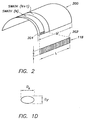
- the slow axis direction corresponds to the movement of the optical head along the longitudinal axis of an imaging drum which parallels the linear direction along the width W (see Figure 2) of the medium 200
- the fast axis direction corresponds to the spinning of a laser beam along the radial direction of the drum, e.g. along a swath (N) of the medium 200.
- the type of light source used is dependent upon the particular media.
- the medium 200 is thermally sensitive, so an appropriate laser light source is used for imaging on that media.
- other sources of electromagnetic energy could be used, as necessary, for various applications.
- the medium 200 is positioned as supported on an external drum (not shown).
- a line of illumination 118 (also referred to as a line of radiation), which is coincident with the medium 200 at the image plane, has a length L and a width Z.
- Each line of illumination 118 contains a predetermined number of sections 202 which, respectively, correspond to some number of pixels on the GLV 110.
- the line of illumination 118 is imaged at an initial position 204 along a first swath (N) on the sheet of medium 200.
- N first swath
- Modulation of pixels is synchronised to the rotational speed of the drum.
- This procedure continues until imaging is complete on swath (N).
- the movement of the line of illumination 118 from swath (N) to (N+1) is facilitated by movement of the imaging head along the longitudinal axis (i.e. the slow axis) of the rotating drum.
- the above-described imaging procedure is repeated for swath (N+1) and all additional swaths until the image is completely transferred onto the medium 200.
- the imaging procedure could also be accomplished by other means such as a spiral scan of the media as well known in the art.
- the GLV operates by diffracting light with the use of moveable ribbons in an array.
- energy from the GLV reaches the image plane when a GLV pixel is not activated.
- a pixel is fully activated, i.e. when alternate ribbons are deflected approximately one-quarter wavelength, then light is diffracted and subsequently blocked from reaching the image plane. Pixels may be partially activated to control the amount of light reaching the image plane.
- One exemplary GLV consists of 1088 individually addressable pixels.
- a one-dimensional GLV array is used, although a two dimensional GLV could be used if desired to create an area of illumination rather than a line of illumination.
- imaging resolutions are available by changing the grouping of the GLV pixels. Also, all pixels of the GLV need not necessarily be used in the formation of an image. For example, if 720 GLV pixels are imaged one-for-one at the image plane to produce a resolution of 2400 image pixels (i.e. writing dots) per inch, then a grouping of two GLV pixels per image plane pixel results in 360 writing dots at a resolution of 1200 dots per inch.
- the imaging system 130 includes the grating light valve 110, a first magnification lens group 112, a stop 114 containing an aperture 132, and a second focusing lens group 116.
- the grating light valve used here allows each pixel 202 to be separately and individually controlled in accordance with signals from control electronics built into the GLV modulator 110. In other words, individual image pixels 202 can be separately diffracted.
- the intensity of each GLV pixel can be electronically controlled by varying the voltage applied to the ribbons, thus controlling their deflection and ultimately the amount of energy that reaches the image plane. Varying the intensity of GLV pixels on the GLV object plane 120 can correct non-uniformity of the line of illumination on the image plane.
- the surface 120 of the grating light valve 110 includes a diffraction grating, i.e. an array of narrow parallel slits or openings which, when white light is projected therethrough, breaks down the white light into all the colours of the spectrum due to the diffraction of light waves as they pass through the openings.
- the diffraction grating produces this spectral effect due to the reinforcement of the light waves from adjacent slits or openings.
- Figure 3 illustrates the effect of the diffraction grating surface 120 on white light received from the light source 102.
- FIG 3 selected components of the imaging head 150 of Figure 1A are depicted to illustrate diffraction of light from the surface 120 of the grating light valve 110.
- Zero order diffracted light is represented by solid lines whereas, positive and negative first order diffracted light is represented by dotted lines. Higher diffractive orders are omitted for simplicity.
- the zero order diffracted light reflected from the object plane 120 of the GLV 110 passes through the first lens group 112 and is directed to, and passes through, the aperture 132.
- the first lens group 112 includes at least one fixed lens and at least one adjustable lens for adjusting the image magnification independent of the image focus.
- the aperture 132 is a single centrally located opening (preferably having an elliptical shape as shown in Figure 1D) on the stop 114. The stop 114 blocks non-zero order diffractive rays while allowing zero order diffractive rays to pass through the aperture 132.
- the principal rays of zero order radiation received from the first lens group 112 are focused in the centre of the aperture 132, and passed to the second lens group 116 (see Fig. 1C).
- the second lens group 116 includes one or more lenses for adjusting the image focus independent of the image magnification.
- the second lens group 116 must contain at least one adjustable lens, and could contain zero, one or more fixed lenses. From the second lens group 116, the rays are focused along a line of radiation 118 (see Figure 2) on the imaging medium 200.
- the use of zero order diffracted light in the present invention produces several benefits. Depth of focus is reduced. Also, the optical design is simplified since only a single aperture is used to pass zero order diffracted light. In contrast, multiple apertures and additional optical components are required for passing higher order diffracted light. Additional lens groups are required to collect first or higher order diffracted light. Furthermore, using zero order diffracted light increases resolution while concurrently improving image quality. No significant grey scale adjustment is necessary for imaging with zero order diffracted light.
- One drawback that a zero order diffraction system has when compared to a first order diffraction system is lower contrast ratio and dynamic range.
- the thermal media used for the preferred digital imaging embodiment is not sensitive to these parameters.
- the aperture is positioned to be at a distance equivalent to the focal length f 1 of the first lens group 112 away from the principal plane of the first lens group 122. Maintaining the distance between the first lens group 112 and the object plane 120 of the modulator 110 is important for cleanly separating the diffractive orders.
- One embodiment of the present invention includes a dual telecentric imaging system. Telecentricity occurs when rays are normal to an incident surface. Prior art imaging systems sometimes exhibit singular telecentricity of the rays at the imaging plane. The benefit of having an imaging system with dual telecentricity is to separate diffractive orders and separate magnification adjustments from focusing adjustments.
- the imaging system 130 of the optical head 150 is shown in a dual telecentric arrangement.
- the imaging system is comprised of two lens groups, first lens group 112 and second lens group 116. Lens group 112 has an effective focal length equal to f 1 and lens group 116 has an effective focal length equal to f 2 .
- Dual telecentricity is achieved when the perpendicular distance between the principal planes of lens groups 112 and 116 is equal to f 1 + f 2 , and the aperture 132 is positioned at a common focal plane, i.e. where the aperture is a distance f 1 from the first lens group 122 and a distance f 2 from the second lens group 116.
- magnification of the system is insensitive to movements of the GLV 110 or imaging medium 200.
- magnification or focus can be adjusted independent of one another.
- lens group 112 positioned a distance f 1 from the object plane 120
- lens group 116 positioned a distance f 2 from the image plane 200 and the distance between first and second lens groups to be the distance f 1 + f 2
- the ratio (f 2 / f 1 ) sets the magnification of the imaging system 130.
- the magnification is adjusted by moving one or more elements of the first lens group 112.
- the focus of the system is adjusted by moving one or more elements of the second lens group 116.
- Every emitter of the diode bar 102 illuminates the entire object plane 120 of the GLV 110. This provides an advantage in that the energy distribution across the object plane 120 is smoothed by the contributions from each diode.
- the long, matched focal lengths of the illumination system 100 have the effect of reducing the divergence of the energy reflected from the GLV 110, which, in turn, improves the depth of focus of the imaging system 130.
- the optical imaging head 150 is preferably used with an external drum imagesetter or platesetter, so that the image is transferred onto a medium supported by the external surface of the drum.
- the optical imaging head 150 could also be used in direct-to-press imaging to project the line of illumination 118 directly onto a plate cylinder of a printing press. In this case, the head would be replicated at each station of the printing press.
- the head is most appropriately used in the above-described applications, it may also be used in an internal drum or capstan style imagesetter or platesetter.
- GLV 110 Due to the fact that a large number of pixels is used to create the GLV 110, it is possible to advantageously employ some number of pixels for uses other than as writing beams without incurring a penalty.
- These other uses include sourcing beams (1) to detect the edge of a plate so as to synchronise the image location with the position of the recording medium, or (2) to sense or to automatically adjust the focus of an imaging system.
- GLV pixels may be actuated to different levels of diffraction efficiency can be used to great advantage.
- a first possible use is to equalise the energy distribution across the GLV. If a nominal energy level is set below the maximum, then individual pixels can be adjusted either up or down to cause all pixels to be equal.
- a second use is to desensitise the effects of pixel placement errors at the boundary between bands of multiple pixels. The pixels located at the boundary between the swathe of multiple pixels can be lowered in intensity and overlapped so as to average the effective position.
- the GLV is cost effective compared with manufacture of other light modulators since the fabrication of the GLV uses standard fabrication methods employed in the semiconductor industry. Also, the pixels of the GLV are accurately located to tight semiconductor standards.
- the GLV is capable of modulating high power levels of radiation.
- the reflective GLV results in a more compact system as compared to an in-line multiple beam system.
- a transmissive modulator could be used to replace the GLV, but one of the trade-off a would be a physically larger system. Due to the scale and materials employed, the GLV is inherently insensitive to damage from shock and vibration. The GLV is also sealed and insignificantly stressed in use, resulting in high reliability.
- the GLV can be used with different wavelength sources.
- the GLV can also be used with both multi-mode and single mode lasers. Further, as compared to single beam methods of writing images, the adjacency of the pixels produced by the GLV reduces the power required to write equivalent images.
Landscapes
- Physics & Mathematics (AREA)
- General Physics & Mathematics (AREA)
- Optics & Photonics (AREA)
- Printers Or Recording Devices Using Electromagnetic And Radiation Means (AREA)
- Laser Beam Printer (AREA)
- Lenses (AREA)
- Exposure And Positioning Against Photoresist Photosensitive Materials (AREA)
- Projection-Type Copiers In General (AREA)
- Electronic Switches (AREA)
- Optical Head (AREA)
Abstract
Description
- a line illumination module (100) for generating a substantially uniform line of radiation;
- a grating light valve (110), forming an object plane, which receives the line of radiation from the line illumination module and generates diffractive orders of modulated radiation;
- a first lens group (112) for receiving the modulated radiation and for adjusting image magnification independent of image focus;
- a second lens group (116) for receiving and passing the magnification-adjusted modulated radiation from the first lens group to the medium in a telecentric fashion, said second lens group adjusting image focus independent of image magnification; and
- a stop (114), placed between the first (112) and second (116) lens groups, having a single aperture (132) for passing zero order diffractive magnification-adjusted modulated radiation and for blocking non-zero order diffractive magnification-adjusted modulated radiation.
Claims (14)
- An optical imaging head for imaging an image onto a medium (200), the imaging head comprising:a line illumination module (100) for generating a substantially uniform line of radiation;a grating light valve (110), forming an object plane, which receives the line of radiation from the line illumination module and generates diffractive orders of modulated radiation;a first lens group (112) for receiving the modulated radiation and for adjusting image magnification independent of image focus;a second lens group (116) for receiving and passing the magnification-adjusted modulated radiation from the first lens group to the medium in a telecentric fashion, said second lens group adjusting image focus independent of image magnification; anda stop (114), placed between the first (112) and second (116) lens groups, having a single aperture (132) for passing zero order diffractive magnification-adjusted modulated radiation and for blocking non-zero order diffractive magnification-adjusted modulated radiation.
- The imaging head according to claim 1 wherein the aperture is elliptical.
- The imaging head according to claim 1 or 2, having dual telecentricity wherein a focal length of the first lens group is f1, the distance between a principal plane of the first lens group and the stop is f1, a focal length of the second lens group is f2, a distance between the stop and a principal plane of the second lens group is f2, and a perpendicular distance between the principal planes of the lens groups is equal to f1 + f2.
- The imaging head according to any of claims 1 to 3 wherein the grating light valve includes control electronics to separately diffract individual sections of the line of radiation in accordance with the image.
- The imaging head according to claim 4 wherein the control electronics varies grating light valve pixel intensities on the object plane to correct non-uniformities in the image.
- The imaging head according to any of claims 1 to 5, wherein the first lens group comprises one or more fixed lenses and one or more adjustable lenses for adjusting the magnification of the image independent of the focus.
- The imaging head according to any of claims 1 to 6, wherein the second lens group comprises at least one adjustable lens for adjusting the focus of the image independent of the magnification.
- The imaging head according to claim 1 wherein the medium is supported on an external drum surface, an internal drum surface, or a planar surface.
- A method for transferring an image to a medium, the method comprising:generating a substantially uniform line of radiation; producing diffractive light from the uniform line of radiation;passing zero order said diffractive light to the medium in a telecentric fashion while blocking non-zero order said diffractive light;adjusting image magnification on the medium independent of image focus in response to the zero order said diffractive light; andadjusting image focus on the medium independent of image magnification in response to the zero order magnification-adjusted diffractive light.
- The method according to claim 9 wherein the uniform line of radiation is telecentric at a diffractive grating surface used for producing said diffractive light.
- The method according to claim 10 further comprising varying pixel intensities on the diffractive grating surface to correct non-uniformities in the image.
- The method according to any of claims 9 to 11, wherein a focal length of a first lens group is f1, a distance between a principal plane of the first lens group and a stop is f1, a focal length of a second lens group is f2, a distance between the stop and a principal plane of the second lens group is f2, and a perpendicular distance between the principal planes of the lens groups is equal to f1 + f2.
- The method according to any of claims 9 to 12, wherein the medium is supported on an external drum surface, an internal drum surface, or a planar surface.
- The method according to any of claims 9 to 13 wherein the medium is thermally sensitive or photosensitive.
Applications Claiming Priority (2)
| Application Number | Priority Date | Filing Date | Title |
|---|---|---|---|
| US420276 | 1989-10-12 | ||
| US09/420,276 US6229650B1 (en) | 1999-10-18 | 1999-10-18 | Optical imaging head having a multiple writing bean source |
Publications (3)
| Publication Number | Publication Date |
|---|---|
| EP1094352A2 true EP1094352A2 (en) | 2001-04-25 |
| EP1094352A3 EP1094352A3 (en) | 2003-12-17 |
| EP1094352B1 EP1094352B1 (en) | 2009-12-23 |
Family
ID=23665816
Family Applications (1)
| Application Number | Title | Priority Date | Filing Date |
|---|---|---|---|
| EP00203618A Expired - Lifetime EP1094352B1 (en) | 1999-10-18 | 2000-10-13 | Optical imaging head having a multiple writing beam source |
Country Status (4)
| Country | Link |
|---|---|
| US (1) | US6229650B1 (en) |
| EP (1) | EP1094352B1 (en) |
| JP (1) | JP4079301B2 (en) |
| DE (1) | DE60043567D1 (en) |
Cited By (3)
| Publication number | Priority date | Publication date | Assignee | Title |
|---|---|---|---|---|
| EP1372014A1 (en) * | 2002-06-12 | 2003-12-17 | Eastman Kodak Company | High-contrast display system with scanned conformal grating device |
| EP2071401A2 (en) | 2006-04-04 | 2009-06-17 | tesa scribos GmbH | Device and method for microstructuring a storage medium and storage medium with a microstructured area |
| EP1596571A3 (en) * | 2004-05-13 | 2009-07-15 | Agfa Corporation | Reduction of imaging artifacts in a platesetter having a diffractive modulator. |
Families Citing this family (63)
| Publication number | Priority date | Publication date | Assignee | Title |
|---|---|---|---|---|
| US6303986B1 (en) | 1998-07-29 | 2001-10-16 | Silicon Light Machines | Method of and apparatus for sealing an hermetic lid to a semiconductor die |
| US6872984B1 (en) | 1998-07-29 | 2005-03-29 | Silicon Light Machines Corporation | Method of sealing a hermetic lid to a semiconductor die at an angle |
| DE60122469T2 (en) * | 2000-02-03 | 2007-05-03 | Kodak Polychrome Graphics Co. Ltd., Norwalk | DEVICE FOR EXPOSING A HEAT-SENSITIVE MEDIUM |
| US6956878B1 (en) | 2000-02-07 | 2005-10-18 | Silicon Light Machines Corporation | Method and apparatus for reducing laser speckle using polarization averaging |
| JP3590334B2 (en) | 2000-08-28 | 2004-11-17 | 大日本スクリーン製造株式会社 | Image recording device |
| EP1202550B1 (en) * | 2000-10-31 | 2006-05-31 | Dainippon Screen Mfg. Co., Ltd. | Laser irradiation device and image recorder |
| US7177081B2 (en) | 2001-03-08 | 2007-02-13 | Silicon Light Machines Corporation | High contrast grating light valve type device |
| US6707591B2 (en) | 2001-04-10 | 2004-03-16 | Silicon Light Machines | Angled illumination for a single order light modulator based projection system |
| US6865346B1 (en) | 2001-06-05 | 2005-03-08 | Silicon Light Machines Corporation | Fiber optic transceiver |
| US6782205B2 (en) | 2001-06-25 | 2004-08-24 | Silicon Light Machines | Method and apparatus for dynamic equalization in wavelength division multiplexing |
| US6639722B2 (en) | 2001-08-15 | 2003-10-28 | Silicon Light Machines | Stress tuned blazed grating light valve |
| US6930364B2 (en) | 2001-09-13 | 2005-08-16 | Silicon Light Machines Corporation | Microelectronic mechanical system and methods |
| US6956995B1 (en) | 2001-11-09 | 2005-10-18 | Silicon Light Machines Corporation | Optical communication arrangement |
| US6800238B1 (en) | 2002-01-15 | 2004-10-05 | Silicon Light Machines, Inc. | Method for domain patterning in low coercive field ferroelectrics |
| US6728023B1 (en) | 2002-05-28 | 2004-04-27 | Silicon Light Machines | Optical device arrays with optimized image resolution |
| US6767751B2 (en) | 2002-05-28 | 2004-07-27 | Silicon Light Machines, Inc. | Integrated driver process flow |
| US7054515B1 (en) | 2002-05-30 | 2006-05-30 | Silicon Light Machines Corporation | Diffractive light modulator-based dynamic equalizer with integrated spectral monitor |
| US6822797B1 (en) | 2002-05-31 | 2004-11-23 | Silicon Light Machines, Inc. | Light modulator structure for producing high-contrast operation using zero-order light |
| US6829258B1 (en) | 2002-06-26 | 2004-12-07 | Silicon Light Machines, Inc. | Rapidly tunable external cavity laser |
| US6714337B1 (en) | 2002-06-28 | 2004-03-30 | Silicon Light Machines | Method and device for modulating a light beam and having an improved gamma response |
| US6813059B2 (en) | 2002-06-28 | 2004-11-02 | Silicon Light Machines, Inc. | Reduced formation of asperities in contact micro-structures |
| US6908201B2 (en) | 2002-06-28 | 2005-06-21 | Silicon Light Machines Corporation | Micro-support structures |
| US7057795B2 (en) | 2002-08-20 | 2006-06-06 | Silicon Light Machines Corporation | Micro-structures with individually addressable ribbon pairs |
| US6801354B1 (en) | 2002-08-20 | 2004-10-05 | Silicon Light Machines, Inc. | 2-D diffraction grating for substantially eliminating polarization dependent losses |
| US6712480B1 (en) | 2002-09-27 | 2004-03-30 | Silicon Light Machines | Controlled curvature of stressed micro-structures |
| US6947459B2 (en) * | 2002-11-25 | 2005-09-20 | Eastman Kodak Company | Organic vertical cavity laser and imaging system |
| US6928207B1 (en) | 2002-12-12 | 2005-08-09 | Silicon Light Machines Corporation | Apparatus for selectively blocking WDM channels |
| US6987600B1 (en) | 2002-12-17 | 2006-01-17 | Silicon Light Machines Corporation | Arbitrary phase profile for better equalization in dynamic gain equalizer |
| US7057819B1 (en) | 2002-12-17 | 2006-06-06 | Silicon Light Machines Corporation | High contrast tilting ribbon blazed grating |
| US6934070B1 (en) | 2002-12-18 | 2005-08-23 | Silicon Light Machines Corporation | Chirped optical MEM device |
| US6927891B1 (en) | 2002-12-23 | 2005-08-09 | Silicon Light Machines Corporation | Tilt-able grating plane for improved crosstalk in 1×N blaze switches |
| US20040145708A1 (en) * | 2003-01-24 | 2004-07-29 | Evans & Sutherland Computer Corporation | Infrared projector |
| US6751001B1 (en) | 2003-01-24 | 2004-06-15 | Evans & Sutherland Computer Corporation | Non-sampled auto-format conversion method |
| US7068372B1 (en) | 2003-01-28 | 2006-06-27 | Silicon Light Machines Corporation | MEMS interferometer-based reconfigurable optical add-and-drop multiplexor |
| US7286764B1 (en) | 2003-02-03 | 2007-10-23 | Silicon Light Machines Corporation | Reconfigurable modulator-based optical add-and-drop multiplexer |
| US6894822B2 (en) * | 2003-02-04 | 2005-05-17 | Silicon Light Machines Corporation | Robust reflective surface for light modulators |
| US7113320B2 (en) | 2003-02-06 | 2006-09-26 | Evans & Sutherland Computer Corporation | GLV based fiber optic transmitter |
| US6947613B1 (en) | 2003-02-11 | 2005-09-20 | Silicon Light Machines Corporation | Wavelength selective switch and equalizer |
| US6922272B1 (en) | 2003-02-14 | 2005-07-26 | Silicon Light Machines Corporation | Method and apparatus for leveling thermal stress variations in multi-layer MEMS devices |
| US7027202B1 (en) | 2003-02-28 | 2006-04-11 | Silicon Light Machines Corp | Silicon substrate as a light modulator sacrificial layer |
| US6829077B1 (en) | 2003-02-28 | 2004-12-07 | Silicon Light Machines, Inc. | Diffractive light modulator with dynamically rotatable diffraction plane |
| US6922273B1 (en) | 2003-02-28 | 2005-07-26 | Silicon Light Machines Corporation | PDL mitigation structure for diffractive MEMS and gratings |
| US6806997B1 (en) | 2003-02-28 | 2004-10-19 | Silicon Light Machines, Inc. | Patterned diffractive light modulator ribbon for PDL reduction |
| US7391973B1 (en) | 2003-02-28 | 2008-06-24 | Silicon Light Machines Corporation | Two-stage gain equalizer |
| US7042611B1 (en) | 2003-03-03 | 2006-05-09 | Silicon Light Machines Corporation | Pre-deflected bias ribbons |
| US7286155B1 (en) | 2003-05-30 | 2007-10-23 | Silicon Light Machines Corporation | Optical engine using one-dimensional MEMS device |
| CN1301857C (en) * | 2003-06-28 | 2007-02-28 | 项建龙 | Light splitting method for realizing Multipath output on laser phototypographic composing machine and its system |
| US7218336B2 (en) * | 2003-09-26 | 2007-05-15 | Silicon Light Machines Corporation | Methods and apparatus for driving illuminators in printing applications |
| US7248278B1 (en) | 2003-12-10 | 2007-07-24 | Silicon Light Machines Corporation | Apparatus and method for laser printing using a spatial light modulator |
| US7489329B2 (en) * | 2004-04-29 | 2009-02-10 | Samsung Electro-Mechanics Co., Ltd. | Scanning apparatus using vibration light modulator |
| US20070144384A1 (en) | 2004-05-19 | 2007-06-28 | Fuji Photo Film Co., Ltd | Image recording method |
| US7265772B2 (en) * | 2004-12-16 | 2007-09-04 | Esko Graphics A/S | Beam illumination system and method for producing printing plates |
| US7573631B1 (en) | 2005-02-22 | 2009-08-11 | Silicon Light Machines Corporation | Hybrid analog/digital spatial light modulator |
| JP2007093947A (en) * | 2005-09-28 | 2007-04-12 | Fujifilm Corp | Inner drum exposure apparatus and exposure method |
| KR100800709B1 (en) * | 2005-10-10 | 2008-02-01 | 삼성전자주식회사 | Video scanning device |
| JP4553313B2 (en) * | 2005-10-31 | 2010-09-29 | 大日本スクリーン製造株式会社 | Image recording device |
| US7576902B2 (en) * | 2006-09-06 | 2009-08-18 | Texas Instruments Incorporated | Spatial light modulator mirror metal having enhanced reflectivity |
| US7891818B2 (en) | 2006-12-12 | 2011-02-22 | Evans & Sutherland Computer Corporation | System and method for aligning RGB light in a single modulator projector |
| US8358317B2 (en) | 2008-05-23 | 2013-01-22 | Evans & Sutherland Computer Corporation | System and method for displaying a planar image on a curved surface |
| US8702248B1 (en) | 2008-06-11 | 2014-04-22 | Evans & Sutherland Computer Corporation | Projection method for reducing interpixel gaps on a viewing surface |
| US8077378B1 (en) | 2008-11-12 | 2011-12-13 | Evans & Sutherland Computer Corporation | Calibration system and method for light modulation device |
| US9641826B1 (en) | 2011-10-06 | 2017-05-02 | Evans & Sutherland Computer Corporation | System and method for displaying distant 3-D stereo on a dome surface |
| CN115437096B (en) * | 2022-09-13 | 2024-06-21 | 山东山科美瑞光电技术有限公司 | Modularized combined double telecentric lens capable of generating multiple amplification factors |
Family Cites Families (11)
| Publication number | Priority date | Publication date | Assignee | Title |
|---|---|---|---|---|
| US4724467A (en) * | 1983-04-11 | 1988-02-09 | Xerox Corporation | Light blocking stop for electro-optic line printers |
| US4872743A (en) | 1983-04-18 | 1989-10-10 | Canon Kabushiki Kaisha | Varifocal optical element |
| US4786918A (en) | 1985-12-12 | 1988-11-22 | Xerox Corporation | Incoherent, optically uncoupled laser arrays for electro-optic line modulators and line printers |
| US4718752A (en) * | 1985-12-23 | 1988-01-12 | Xerox Corporation | Interpixel null suppression for polarized optical image bars |
| IL107508A (en) * | 1993-11-05 | 1996-12-05 | Orbotech Ltd | Method and apparatus for recording on optically-sensitive media |
| US5521748A (en) | 1994-06-16 | 1996-05-28 | Eastman Kodak Company | Light modulator with a laser or laser array for exposing image data |
| KR970048631A (en) * | 1995-12-27 | 1997-07-29 | 쇼이찌로 요시다 | Variable telecentric optics |
| US5802034A (en) | 1996-12-09 | 1998-09-01 | Gelbart; Daniel | Multi-track optical read/write head |
| US5991065A (en) * | 1996-12-10 | 1999-11-23 | Eastman Kodak Company | Addressable electro-optic modulator with periodically poled domain regions |
| US5900981A (en) | 1997-04-15 | 1999-05-04 | Scitex Corporation Ltd. | Optical system for illuminating a spatial light modulator |
| US6147789A (en) * | 1998-05-04 | 2000-11-14 | Gelbart; Daniel | High speed deformable mirror light valve |
-
1999
- 1999-10-18 US US09/420,276 patent/US6229650B1/en not_active Expired - Fee Related
-
2000
- 2000-10-11 JP JP2000310306A patent/JP4079301B2/en not_active Expired - Fee Related
- 2000-10-13 DE DE60043567T patent/DE60043567D1/en not_active Expired - Lifetime
- 2000-10-13 EP EP00203618A patent/EP1094352B1/en not_active Expired - Lifetime
Cited By (5)
| Publication number | Priority date | Publication date | Assignee | Title |
|---|---|---|---|---|
| EP1372014A1 (en) * | 2002-06-12 | 2003-12-17 | Eastman Kodak Company | High-contrast display system with scanned conformal grating device |
| CN100380229C (en) * | 2002-06-12 | 2008-04-09 | 伊斯曼柯达公司 | High-contrast display system with scanned conformal grating device |
| EP1596571A3 (en) * | 2004-05-13 | 2009-07-15 | Agfa Corporation | Reduction of imaging artifacts in a platesetter having a diffractive modulator. |
| EP2071401A2 (en) | 2006-04-04 | 2009-06-17 | tesa scribos GmbH | Device and method for microstructuring a storage medium and storage medium with a microstructured area |
| US8120996B2 (en) | 2006-04-04 | 2012-02-21 | Tesa Scribos Gmbh | Device and method for microstructuring a storage medium and storage medium comprising a microstructured region |
Also Published As
| Publication number | Publication date |
|---|---|
| EP1094352A3 (en) | 2003-12-17 |
| JP4079301B2 (en) | 2008-04-23 |
| DE60043567D1 (en) | 2010-02-04 |
| JP2001162866A (en) | 2001-06-19 |
| EP1094352B1 (en) | 2009-12-23 |
| US6229650B1 (en) | 2001-05-08 |
Similar Documents
| Publication | Publication Date | Title |
|---|---|---|
| US6229650B1 (en) | Optical imaging head having a multiple writing bean source | |
| EP1193539B1 (en) | Illumination system for use in imaging systems | |
| EP1480441B1 (en) | Method and apparatus for multi-track imaging using single-mode beams and diffraction-limited optics | |
| US5923359A (en) | Internal drum scophony raster recording device | |
| US8928720B2 (en) | Apparatus and method of scanning light using an array of light sources | |
| US20060039053A1 (en) | Light modulator type multi-beam scanning apparatus using dichroic slit | |
| US7868909B2 (en) | Method and apparatus for multi-beam exposure | |
| US7348111B2 (en) | Reduction of imaging artifacts in a platesetter having a diffractive modulator | |
| US6552741B2 (en) | Optical scanning device, image scanning method and photographic processing device | |
| US20050105154A1 (en) | Scanning apparatus using light modulator | |
| EP1184707B1 (en) | Image recorder | |
| KR100567090B1 (en) | Light Beam Injection Device | |
| JP2006085072A (en) | Multi-beam exposure device | |
| JP2006085071A (en) | Multi-beam exposure device | |
| JP2006085073A (en) | Multi-beam exposure device | |
| JP2006085070A (en) | Multi-beam exposure method and device | |
| KR100813960B1 (en) | Scanning optics and image forming apparatus employing the same | |
| US20060119692A1 (en) | Order separation and multibeam formation-based printing apparatus using optical modulator | |
| JP2743858B2 (en) | Optical printer | |
| USRE38297E1 (en) | Internal drum scophony raster recording device | |
| KR20050114939A (en) | Apparatus and method for scanning constant beam | |
| EP1177676B1 (en) | Internal drum scophony raster recording device | |
| JP2005352439A (en) | Optical recording apparatus using one-dimensional diffractive light modulator | |
| KR100619360B1 (en) | Multiple light source scanning device using optical modulator | |
| JP2003066540A (en) | Image exposure device and image exposure method |
Legal Events
| Date | Code | Title | Description |
|---|---|---|---|
| PUAI | Public reference made under article 153(3) epc to a published international application that has entered the european phase |
Free format text: ORIGINAL CODE: 0009012 |
|
| AK | Designated contracting states |
Kind code of ref document: A2 Designated state(s): AT BE CH CY DE DK ES FI FR GB GR IE IT LI LU MC NL PT SE |
|
| AX | Request for extension of the european patent |
Free format text: AL;LT;LV;MK;RO;SI |
|
| PUAL | Search report despatched |
Free format text: ORIGINAL CODE: 0009013 |
|
| AK | Designated contracting states |
Kind code of ref document: A3 Designated state(s): AT BE CH CY DE DK ES FI FR GB GR IE IT LI LU MC NL PT SE |
|
| AX | Request for extension of the european patent |
Extension state: AL LT LV MK RO SI |
|
| RIC1 | Information provided on ipc code assigned before grant |
Ipc: 7G 06K 15/12 B Ipc: 7H 04N 1/191 B Ipc: 7B 41J 2/465 B Ipc: 7G 02B 26/10 B Ipc: 7G 02B 27/44 A |
|
| 17P | Request for examination filed |
Effective date: 20040617 |
|
| AKX | Designation fees paid |
Designated state(s): DE FR GB |
|
| 17Q | First examination report despatched |
Effective date: 20040928 |
|
| 17Q | First examination report despatched |
Effective date: 20040928 |
|
| GRAP | Despatch of communication of intention to grant a patent |
Free format text: ORIGINAL CODE: EPIDOSNIGR1 |
|
| GRAS | Grant fee paid |
Free format text: ORIGINAL CODE: EPIDOSNIGR3 |
|
| GRAA | (expected) grant |
Free format text: ORIGINAL CODE: 0009210 |
|
| AK | Designated contracting states |
Kind code of ref document: B1 Designated state(s): DE FR GB |
|
| REG | Reference to a national code |
Ref country code: GB Ref legal event code: FG4D |
|
| REF | Corresponds to: |
Ref document number: 60043567 Country of ref document: DE Date of ref document: 20100204 Kind code of ref document: P |
|
| PLBE | No opposition filed within time limit |
Free format text: ORIGINAL CODE: 0009261 |
|
| STAA | Information on the status of an ep patent application or granted ep patent |
Free format text: STATUS: NO OPPOSITION FILED WITHIN TIME LIMIT |
|
| PGFP | Annual fee paid to national office [announced via postgrant information from national office to epo] |
Ref country code: FR Payment date: 20100903 Year of fee payment: 11 |
|
| 26N | No opposition filed |
Effective date: 20100924 |
|
| PGFP | Annual fee paid to national office [announced via postgrant information from national office to epo] |
Ref country code: GB Payment date: 20100827 Year of fee payment: 11 |
|
| PGFP | Annual fee paid to national office [announced via postgrant information from national office to epo] |
Ref country code: DE Payment date: 20100827 Year of fee payment: 11 |
|
| GBPC | Gb: european patent ceased through non-payment of renewal fee |
Effective date: 20111013 |
|
| REG | Reference to a national code |
Ref country code: FR Ref legal event code: ST Effective date: 20120629 |
|
| PG25 | Lapsed in a contracting state [announced via postgrant information from national office to epo] |
Ref country code: DE Free format text: LAPSE BECAUSE OF NON-PAYMENT OF DUE FEES Effective date: 20120501 |
|
| REG | Reference to a national code |
Ref country code: DE Ref legal event code: R119 Ref document number: 60043567 Country of ref document: DE Effective date: 20120501 |
|
| PG25 | Lapsed in a contracting state [announced via postgrant information from national office to epo] |
Ref country code: FR Free format text: LAPSE BECAUSE OF NON-PAYMENT OF DUE FEES Effective date: 20111102 Ref country code: GB Free format text: LAPSE BECAUSE OF NON-PAYMENT OF DUE FEES Effective date: 20111013 |