EP1098200B1 - Dispositif de réglage pour la planarisation de jeux de pointes d'une carte à pointes - Google Patents
Dispositif de réglage pour la planarisation de jeux de pointes d'une carte à pointes Download PDFInfo
- Publication number
- EP1098200B1 EP1098200B1 EP00123270A EP00123270A EP1098200B1 EP 1098200 B1 EP1098200 B1 EP 1098200B1 EP 00123270 A EP00123270 A EP 00123270A EP 00123270 A EP00123270 A EP 00123270A EP 1098200 B1 EP1098200 B1 EP 1098200B1
- Authority
- EP
- European Patent Office
- Prior art keywords
- needle
- card
- probe card
- adjusting device
- adjusting unit
- Prior art date
- Legal status (The legal status is an assumption and is not a legal conclusion. Google has not performed a legal analysis and makes no representation as to the accuracy of the status listed.)
- Expired - Lifetime
Links
Images

Classifications
-
- G—PHYSICS
- G01—MEASURING; TESTING
- G01R—MEASURING ELECTRIC VARIABLES; MEASURING MAGNETIC VARIABLES
- G01R31/00—Arrangements for testing electric properties; Arrangements for locating electric faults; Arrangements for electrical testing characterised by what is being tested not provided for elsewhere
- G01R31/28—Testing of electronic circuits, e.g. by signal tracer
- G01R31/2851—Testing of integrated circuits [IC]
- G01R31/2886—Features relating to contacting the IC under test, e.g. probe heads; chucks
- G01R31/2887—Features relating to contacting the IC under test, e.g. probe heads; chucks involving moving the probe head or the IC under test; docking stations
-
- H—ELECTRICITY
- H10—SEMICONDUCTOR DEVICES; ELECTRIC SOLID-STATE DEVICES NOT OTHERWISE PROVIDED FOR
- H10P—GENERIC PROCESSES OR APPARATUS FOR THE MANUFACTURE OR TREATMENT OF DEVICES COVERED BY CLASS H10
- H10P74/00—Testing or measuring during manufacture or treatment of wafers, substrates or devices
-
- G—PHYSICS
- G01—MEASURING; TESTING
- G01R—MEASURING ELECTRIC VARIABLES; MEASURING MAGNETIC VARIABLES
- G01R3/00—Apparatus or processes specially adapted for the manufacture or maintenance of measuring instruments, e.g. of probe tips
Definitions
- the present invention relates to a probe card adjusting device for planarizing needle sets of a probe card (also referred to as a probe card) with respect to a to be contacted wafer, in which the probe card with a as a contact interface to a test head serving board connected is.
- a probe card also referred to as a probe card
- US 5,861,859 describes an automatic planarization system for test cards, in which a test card is adjusted with respect to a wafer surface by first three tips of the test card, two of which are height-adjustable are aligned to the wafer surface.
- US-A-5 191 708 discloses a method of manufacturing a probe head for a semiconductor LSI monitor described. Probes go off a probe card via a wiring substrate.
- Needle sets of needle cards are known to be the electrical Connection between individual contact pads or pads of chips on the one hand and a test head ago, in order to improve the functionality to check the chips on the wafer.
- Needle sets need namely to the order of 1/4 micron accurate adjusted their respective assigned contact pads of the chips become.
- the probe card in addition to the static adjustment the probe card is also dynamic relative to the chips Components must be considered, for example by thermal expansion of the probe card during a Warming or cooling via a wafer holding device, also called "Chuck", are conditional.
- Other dynamic components are due to aging effects of the needle cards attributed to which the needle sets mostly are glued. But the dynamic components can as well very short time constants, such as shocks, to have.
- needle card glued needle sets are these not yet or only by subsequent bending everyone single needle adjusted, resulting in the required accuracy up to 1/4 micron a considerable cost and time means.
- the needle sets on so-called Spacetransformern Applied they can with the help of simple Adjusted screws, but with what the specified accuracy can hardly be reached.
- a probe card adjustment device to create with the the needle sets a probe card readily with respect to a to be contacted Wafers can be planarized.
- a probe card adjustment device of the type mentioned in the present invention achieved by that the probe card has a separate, dynamically operating Adjustment unit is connected to the board and that the adjustment unit via a sense line and an active line are connected to a control unit.
- this adjustment unit of at least one Piezo element constructed. But it can also be a variety of Piezo elements comprise in the edge region of the probe card attack at this.
- the planarity of the probe card can readily be in place and Place to be made by dynamic adjustment.
- The is called a needle card misalignment, for example, by Thermal expansion of the probe card or by short-term vibration caused, can be corrected easily. Due to the dynamic adjustability of the probe card let the parallelism between probe card and wafer Correct when contacting it beyond the edge of the wafer.
- the adjustment unit can move in directions that are essentially perpendicular to the spanned by the needle card surface Level, and / or in directions that are essentially lie in this plane, act.
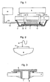
- Fig. 1 shows a probe card 1, by means of screws 4 between a board 3 and a window of a stiffening second is stored.
- the board 3 serves as a contact interface to a test head 5, with the help of test signals to individual needles 6 of the probe card 1 can be supplied.
- Fig. 2 shows the structure of such a needle 6, wherein here the needle 6 contacts a pad 7 on a chip 8 of a wafer.
- test head 5 The electrical connection between the test head 5 and the Board 3 is indicated by connecting buses 9, while between the board 3 and the individual needles 6 connecting wires 10 are guided.
- the screws 4 represent a mechanical adjustment unit, because by twisting parallelism between the probe card 1 and the surface of a contacted by the needles 6 Chips can be approximated.
- piezoelectric elements 11 provided, each via a sensor or Sense line 12 and an active line 13 with a control unit 14 are connected. Is through the piezo elements 11 a misalignment between the needles 6 of the probe card. 1 and the wafer surface is detected, this becomes misalignment reported via the sense line 12 to the computer 14. This will compensate for the misalignment necessary corrections to then appropriate Deliver signals via the active line 13 to the piezo elements 11.
- the lines 12, 13 form with the control unit 14 a Contact test loop, with the help of appropriate Dillatation or contraction of the piezo elements 11, the desired Adjustment can be made.
- the zero position of the probe card can be performed after a Adjustment be adjusted by means of screws 4, so that make the piezoelectric elements 11 only readjustments need.
- FIG. 3 shows a further embodiment of the invention, in which the probe card 1 with a set of needles 6 in one Window of a stiffening 2 is located.
- the Piezo elements 11 between this stiffener 2 and a Board 3 is arranged so that the adjustment alone on the Piezo elements 3 and not make additional screws 4 is.
- FIG. 3 in the same How the embodiment of Fig. 1 constructed: Again, the piezo elements 11 via corresponding lines (not shown separately in FIG. 3) with a control unit connected.
- Fig. 4 shows an embodiment in which an arrangement of several needle cards 1, which in a stiffening 2 acting solid frame are attached and laterally against this frame or against each other by piezoelectric elements 11th can be moved.
- Such laterally acting piezoelectric elements can easily also with the vertically acting piezoelectric elements of FIG. 1 and 3 are combined when, for example, in FIG. 1 between the stiffener 2 and the probe card 1 in appropriate Be attached.
Landscapes
- Engineering & Computer Science (AREA)
- Computer Hardware Design (AREA)
- Microelectronics & Electronic Packaging (AREA)
- General Engineering & Computer Science (AREA)
- Physics & Mathematics (AREA)
- General Physics & Mathematics (AREA)
- Testing Or Measuring Of Semiconductors Or The Like (AREA)
- Measuring Leads Or Probes (AREA)
- Testing Of Individual Semiconductor Devices (AREA)
- Tests Of Electronic Circuits (AREA)
Claims (5)
- Dispositif de réglage de carte à pointes pour la planarisation de jeux (6) de pointes d'une carte (1) à pointes par rapport à une tranche (8) à contacter, dans lequel la carte (1) à pointes est reliée à une platine (3) servant d'interface de contact avec une tête (5) de test,
caractérisé en ce quela carte (1) à pointes est reliée à la platine (3) par une unité (4, 11) de réglage distincte fonctionnant de manière dynamique, etl'unité (4, 11) de réglage est reliée par une ligne (12) de détecteur et par une ligne (13) active à une unité (14) de commande. - Dispositif de réglage de carte à pointes suivant la revendication 1,
caractérisé en ce que l'unité de réglage est constituée d'au moins un élément (11) piézoélectrique. - Dispositif de réglage de carte à pointes suivant la revendication 2,
caractérisé en ce que l'unité de réglage a une pluralité d'éléments (12) piézoélectriques qui attaquent la carte (1) à pointes dans sa région de bord. - Dispositif de réglage de carte à pointes suivant l'une des revendications 1 à 3,
caractérisé en ce qu'il est prévu, en plus, un renfort (2) entre la carte (1) à pointe et l'unité (11) de réglage. - Dispositif de réglage de carte à pointes suivant l'une des revendications 1 à 4,
caractérisé en ce que l'unité (4, 11) de réglage agit dans des directions qui sont sensiblement perpendiculaires au plan passant par la surface de la carte à pointes et/ou dans des directions qui sont sensiblement dans ce plan.
Applications Claiming Priority (2)
| Application Number | Priority Date | Filing Date | Title |
|---|---|---|---|
| DE19952943A DE19952943C2 (de) | 1999-11-03 | 1999-11-03 | Nadelkarten-Justageeinrichtung zur Planarisierung von Nadelsätzen einer Nadelkarte |
| DE19952943 | 1999-11-03 |
Publications (3)
| Publication Number | Publication Date |
|---|---|
| EP1098200A2 EP1098200A2 (fr) | 2001-05-09 |
| EP1098200A3 EP1098200A3 (fr) | 2003-08-13 |
| EP1098200B1 true EP1098200B1 (fr) | 2005-07-06 |
Family
ID=7927803
Family Applications (1)
| Application Number | Title | Priority Date | Filing Date |
|---|---|---|---|
| EP00123270A Expired - Lifetime EP1098200B1 (fr) | 1999-11-03 | 2000-10-26 | Dispositif de réglage pour la planarisation de jeux de pointes d'une carte à pointes |
Country Status (7)
| Country | Link |
|---|---|
| US (1) | US6674627B1 (fr) |
| EP (1) | EP1098200B1 (fr) |
| JP (1) | JP2001189354A (fr) |
| KR (1) | KR20010051378A (fr) |
| CN (1) | CN1196935C (fr) |
| DE (2) | DE19952943C2 (fr) |
| TW (1) | TW548411B (fr) |
Cited By (4)
| Publication number | Priority date | Publication date | Assignee | Title |
|---|---|---|---|---|
| US7737709B2 (en) | 2000-03-17 | 2010-06-15 | Formfactor, Inc. | Methods for planarizing a semiconductor contactor |
| US7948252B2 (en) | 2001-07-11 | 2011-05-24 | Formfactor, Inc. | Multilayered probe card |
| US8373428B2 (en) | 1993-11-16 | 2013-02-12 | Formfactor, Inc. | Probe card assembly and kit, and methods of making same |
| US8485418B2 (en) | 1995-05-26 | 2013-07-16 | Formfactor, Inc. | Method of wirebonding that utilizes a gas flow within a capillary from which a wire is played out |
Families Citing this family (22)
| Publication number | Priority date | Publication date | Assignee | Title |
|---|---|---|---|---|
| DE10056882C2 (de) * | 2000-11-16 | 2003-06-05 | Infineon Technologies Ag | Verfahren zum Kalibrieren eines Testsystems für Halbleiterbauelemente und Testsubstrat |
| US7071714B2 (en) | 2001-11-02 | 2006-07-04 | Formfactor, Inc. | Method and system for compensating for thermally induced motion of probe cards |
| US6972578B2 (en) | 2001-11-02 | 2005-12-06 | Formfactor, Inc. | Method and system for compensating thermally induced motion of probe cards |
| JP2003222654A (ja) * | 2002-01-30 | 2003-08-08 | Tokyo Electron Ltd | プローブ装置 |
| US20050110004A1 (en) * | 2003-11-24 | 2005-05-26 | International Business Machines Corporation | Magnetic tunnel junction with improved tunneling magneto-resistance |
| US7071715B2 (en) * | 2004-01-16 | 2006-07-04 | Formfactor, Inc. | Probe card configuration for low mechanical flexural strength electrical routing substrates |
| DE102004023987B4 (de) * | 2004-05-14 | 2008-06-19 | Feinmetall Gmbh | Elektrische Prüfeinrichtung |
| US7471094B2 (en) * | 2005-06-24 | 2008-12-30 | Formfactor, Inc. | Method and apparatus for adjusting a multi-substrate probe structure |
| US7671614B2 (en) * | 2005-12-02 | 2010-03-02 | Formfactor, Inc. | Apparatus and method for adjusting an orientation of probes |
| US20070176615A1 (en) * | 2006-01-27 | 2007-08-02 | Xandex, Inc. | Active probe contact array management |
| DE102006018474A1 (de) * | 2006-04-19 | 2007-10-25 | Infineon Technologies Ag | Testvorrichtung für Halbleiterelemente auf einem Halbleiterwafer sowie ein Testverfahren unter Verwendung der Testvorrichtung |
| DE202007016398U1 (de) | 2006-11-27 | 2008-02-21 | Feinmetall Gmbh | Kontaktiervorrichtung zum Kontaktieren eines zu prüfenden elektrischen Prüflings |
| JP2008134170A (ja) * | 2006-11-29 | 2008-06-12 | Micronics Japan Co Ltd | 電気的接続装置 |
| JP5190195B2 (ja) * | 2006-11-29 | 2013-04-24 | 株式会社日本マイクロニクス | 電気的接続装置 |
| KR100790817B1 (ko) * | 2006-12-06 | 2008-01-03 | 삼성전자주식회사 | 반도체 제조관리 시스템 |
| US7764076B2 (en) * | 2007-02-20 | 2010-07-27 | Centipede Systems, Inc. | Method and apparatus for aligning and/or leveling a test head |
| JP5643476B2 (ja) * | 2008-04-16 | 2014-12-17 | 日本電子材料株式会社 | 二重弾性機構プローブカード |
| US8004296B2 (en) * | 2008-08-19 | 2011-08-23 | Centipede Systems, Inc. | Probe head apparatus for testing semiconductors |
| KR101645167B1 (ko) * | 2010-06-01 | 2016-08-03 | 리노공업주식회사 | 피치 변환기 및 이를 포함하는 프로브 카드 |
| CN104858769B (zh) * | 2014-02-26 | 2018-12-18 | 盛美半导体设备(上海)有限公司 | 相对距离测量装置及方法 |
| CN115036763A (zh) * | 2022-06-24 | 2022-09-09 | 上海御渡半导体科技有限公司 | 一种整体式的线缆转接装置及其安装方法 |
| KR102909266B1 (ko) * | 2023-11-28 | 2026-01-08 | 케이이아이앤드에스피 주식회사 | 비접촉식 피에조 프로브 하강변위 조정장치 |
Family Cites Families (12)
| Publication number | Priority date | Publication date | Assignee | Title |
|---|---|---|---|---|
| US3963985A (en) | 1974-12-12 | 1976-06-15 | International Business Machines Corporation | Probe device having probe heads and method of adjusting distances between probe heads |
| GB2014315B (en) * | 1978-01-30 | 1983-02-02 | Texas Instruments Inc | Determining probe contact |
| JP2928592B2 (ja) * | 1990-06-20 | 1999-08-03 | 株式会社日立製作所 | 半導体lsi検査装置用プローブヘッドの製造方法および検査装置 |
| JP3219844B2 (ja) * | 1992-06-01 | 2001-10-15 | 東京エレクトロン株式会社 | プローブ装置 |
| US5422574A (en) * | 1993-01-14 | 1995-06-06 | Probe Technology Corporation | Large scale protrusion membrane for semiconductor devices under test with very high pin counts |
| US5974662A (en) * | 1993-11-16 | 1999-11-02 | Formfactor, Inc. | Method of planarizing tips of probe elements of a probe card assembly |
| KR100248569B1 (ko) * | 1993-12-22 | 2000-03-15 | 히가시 데쓰로 | 프로우브장치 |
| JPH0883825A (ja) * | 1994-09-09 | 1996-03-26 | Tokyo Electron Ltd | プローブ装置 |
| JP3838381B2 (ja) * | 1995-11-22 | 2006-10-25 | 株式会社アドバンテスト | プローブカード |
| US5861759A (en) * | 1997-01-29 | 1999-01-19 | Tokyo Electron Limited | Automatic probe card planarization system |
| JPH1123615A (ja) * | 1997-05-09 | 1999-01-29 | Hitachi Ltd | 接続装置および検査システム |
| JP3090132B2 (ja) * | 1998-12-18 | 2000-09-18 | 株式会社日立製作所 | プローブヘッドの製造方法 |
-
1999
- 1999-11-03 DE DE19952943A patent/DE19952943C2/de not_active Expired - Fee Related
-
2000
- 2000-10-26 DE DE50010659T patent/DE50010659D1/de not_active Expired - Fee Related
- 2000-10-26 EP EP00123270A patent/EP1098200B1/fr not_active Expired - Lifetime
- 2000-11-01 KR KR1020000064569A patent/KR20010051378A/ko not_active Ceased
- 2000-11-01 JP JP2000334568A patent/JP2001189354A/ja active Pending
- 2000-11-02 TW TW089123085A patent/TW548411B/zh not_active IP Right Cessation
- 2000-11-03 US US09/705,599 patent/US6674627B1/en not_active Expired - Lifetime
- 2000-11-03 CN CNB001355236A patent/CN1196935C/zh not_active Expired - Fee Related
Cited By (5)
| Publication number | Priority date | Publication date | Assignee | Title |
|---|---|---|---|---|
| US8373428B2 (en) | 1993-11-16 | 2013-02-12 | Formfactor, Inc. | Probe card assembly and kit, and methods of making same |
| US8485418B2 (en) | 1995-05-26 | 2013-07-16 | Formfactor, Inc. | Method of wirebonding that utilizes a gas flow within a capillary from which a wire is played out |
| US7737709B2 (en) | 2000-03-17 | 2010-06-15 | Formfactor, Inc. | Methods for planarizing a semiconductor contactor |
| US8427183B2 (en) | 2000-03-17 | 2013-04-23 | Formfactor, Inc. | Probe card assembly having an actuator for bending the probe substrate |
| US7948252B2 (en) | 2001-07-11 | 2011-05-24 | Formfactor, Inc. | Multilayered probe card |
Also Published As
| Publication number | Publication date |
|---|---|
| EP1098200A3 (fr) | 2003-08-13 |
| JP2001189354A (ja) | 2001-07-10 |
| CN1300943A (zh) | 2001-06-27 |
| CN1196935C (zh) | 2005-04-13 |
| KR20010051378A (ko) | 2001-06-25 |
| TW548411B (en) | 2003-08-21 |
| DE50010659D1 (de) | 2005-08-11 |
| EP1098200A2 (fr) | 2001-05-09 |
| DE19952943C2 (de) | 2003-07-03 |
| US6674627B1 (en) | 2004-01-06 |
| DE19952943A1 (de) | 2001-06-13 |
Similar Documents
| Publication | Publication Date | Title |
|---|---|---|
| EP1098200B1 (fr) | Dispositif de réglage pour la planarisation de jeux de pointes d'une carte à pointes | |
| DE69020077T2 (de) | Integrierte Schaltungskarte. | |
| EP0369112B1 (fr) | Adaptateur pour appareil électronique de contrôle des circuits imprimés et équipement semblable | |
| DE69926241T2 (de) | Leiterplatten-verbindungsvorrichtung und herstellungsverfahren | |
| DE19648475B4 (de) | Kontaktstruktur, Prüfkarten und Herstellungsverfahren | |
| DE4133769C2 (de) | Montagesystem zur Ankopplung von Testplatten für die Aufnahme zu testender elektronischer Bauelemente an ein Halbleitertestsystem | |
| DE69302400T2 (de) | Testanordnung mit filmadaptor fuer leiterplatten | |
| DE69223906T2 (de) | Verfahren zur Herstellung invertierter IC's und IC-Moduln mit einem solcher IC's | |
| DE19837138B4 (de) | Prüfkarte zum Prüfen von Chips mit integrierten Schaltungen | |
| DE102007039728B4 (de) | Tastkopfanordnung | |
| EP1152368B1 (fr) | Carte à puce | |
| DE19835840B4 (de) | Herstellungsverfahren für einen Halbleiterchip | |
| WO1998012747A1 (fr) | Circuit integre muni d'un boitier le contenant | |
| EP0283545A1 (fr) | Arrangement des pointes de contact pour la connexion électrique d'un dispositif d'essai avec la surface circulaire de contact d'un spécimen | |
| DE2903517A1 (de) | Messfuehler und damit ausgestattete testanordnung sowie damit durchzufuehrendes testverfahren | |
| EP1186035A1 (fr) | Composant electronique a structures de contact souples et procede de fabrication d'un tel composant | |
| WO2005091366A2 (fr) | Module a semi-conducteur avec substrat de couplage et procede de realisation | |
| EP1111397B1 (fr) | Dispositif pour tester des pouces avec un circuit intégré | |
| DE69019436T2 (de) | Adapter für integrierte Schaltkreiselemente und Verfahren unter Verwendung des Adapters zur Prüfung von zusammengebauten Elementen. | |
| WO2000041241A1 (fr) | Ensemble semi-conducteur integre verticalement | |
| EP0005727A1 (fr) | Sonde de touche pour déterminer la position de structures électriquement conductrices | |
| DE112005003731B4 (de) | Verfahren zur Montage einer elektrischen Verbindungsvorrichtung | |
| DE69430036T2 (de) | Testvorrichtung für integrierte Schaltungen | |
| DE69325181T2 (de) | Halbleitervorrichtung | |
| DE68906982T2 (de) | Adapterrahmen zum pruefen von gedruckten schaltungen hoher dichte. |
Legal Events
| Date | Code | Title | Description |
|---|---|---|---|
| PUAI | Public reference made under article 153(3) epc to a published international application that has entered the european phase |
Free format text: ORIGINAL CODE: 0009012 |
|
| AK | Designated contracting states |
Kind code of ref document: A2 Designated state(s): AT BE CH CY DE DK ES FI FR GB GR IE IT LI LU MC NL PT SE |
|
| AX | Request for extension of the european patent |
Free format text: AL;LT;LV;MK;RO;SI |
|
| PUAL | Search report despatched |
Free format text: ORIGINAL CODE: 0009013 |
|
| AK | Designated contracting states |
Designated state(s): AT BE CH CY DE DK ES FI FR GB GR IE IT LI LU MC NL PT SE |
|
| AX | Request for extension of the european patent |
Extension state: AL LT LV MK RO SI |
|
| 17P | Request for examination filed |
Effective date: 20040127 |
|
| AKX | Designation fees paid |
Designated state(s): DE FR GB IE IT NL |
|
| 17Q | First examination report despatched |
Effective date: 20040706 |
|
| GRAP | Despatch of communication of intention to grant a patent |
Free format text: ORIGINAL CODE: EPIDOSNIGR1 |
|
| GRAS | Grant fee paid |
Free format text: ORIGINAL CODE: EPIDOSNIGR3 |
|
| GRAA | (expected) grant |
Free format text: ORIGINAL CODE: 0009210 |
|
| AK | Designated contracting states |
Kind code of ref document: B1 Designated state(s): DE FR GB IE IT NL |
|
| REG | Reference to a national code |
Ref country code: GB Ref legal event code: FG4D Free format text: NOT ENGLISH |
|
| REG | Reference to a national code |
Ref country code: IE Ref legal event code: FG4D Free format text: LANGUAGE OF EP DOCUMENT: GERMAN |
|
| REF | Corresponds to: |
Ref document number: 50010659 Country of ref document: DE Date of ref document: 20050811 Kind code of ref document: P |
|
| GBT | Gb: translation of ep patent filed (gb section 77(6)(a)/1977) |
Effective date: 20050914 |
|
| PGFP | Annual fee paid to national office [announced via postgrant information from national office to epo] |
Ref country code: NL Payment date: 20051013 Year of fee payment: 6 |
|
| ET | Fr: translation filed | ||
| PLBE | No opposition filed within time limit |
Free format text: ORIGINAL CODE: 0009261 |
|
| STAA | Information on the status of an ep patent application or granted ep patent |
Free format text: STATUS: NO OPPOSITION FILED WITHIN TIME LIMIT |
|
| 26N | No opposition filed |
Effective date: 20060407 |
|
| PG25 | Lapsed in a contracting state [announced via postgrant information from national office to epo] |
Ref country code: NL Free format text: LAPSE BECAUSE OF NON-PAYMENT OF DUE FEES Effective date: 20070501 |
|
| NLV4 | Nl: lapsed or anulled due to non-payment of the annual fee |
Effective date: 20070501 |
|
| PGFP | Annual fee paid to national office [announced via postgrant information from national office to epo] |
Ref country code: IT Payment date: 20071024 Year of fee payment: 8 |
|
| PGFP | Annual fee paid to national office [announced via postgrant information from national office to epo] |
Ref country code: FR Payment date: 20071016 Year of fee payment: 8 Ref country code: GB Payment date: 20071023 Year of fee payment: 8 |
|
| PGFP | Annual fee paid to national office [announced via postgrant information from national office to epo] |
Ref country code: DE Payment date: 20071211 Year of fee payment: 8 |
|
| GBPC | Gb: european patent ceased through non-payment of renewal fee |
Effective date: 20081026 |
|
| REG | Reference to a national code |
Ref country code: IE Ref legal event code: MM4A |
|
| REG | Reference to a national code |
Ref country code: FR Ref legal event code: ST Effective date: 20090630 |
|
| PG25 | Lapsed in a contracting state [announced via postgrant information from national office to epo] |
Ref country code: DE Free format text: LAPSE BECAUSE OF NON-PAYMENT OF DUE FEES Effective date: 20090501 Ref country code: IT Free format text: LAPSE BECAUSE OF NON-PAYMENT OF DUE FEES Effective date: 20081026 |
|
| PGFP | Annual fee paid to national office [announced via postgrant information from national office to epo] |
Ref country code: IE Payment date: 20071023 Year of fee payment: 8 |
|
| PG25 | Lapsed in a contracting state [announced via postgrant information from national office to epo] |
Ref country code: IE Free format text: LAPSE BECAUSE OF NON-PAYMENT OF DUE FEES Effective date: 20081027 Ref country code: FR Free format text: LAPSE BECAUSE OF NON-PAYMENT OF DUE FEES Effective date: 20081031 |
|
| PG25 | Lapsed in a contracting state [announced via postgrant information from national office to epo] |
Ref country code: GB Free format text: LAPSE BECAUSE OF NON-PAYMENT OF DUE FEES Effective date: 20081026 |