EP1107095B1 - Procédé d'alimentation de circuits intégrés à double tension - Google Patents
Procédé d'alimentation de circuits intégrés à double tension Download PDFInfo
- Publication number
- EP1107095B1 EP1107095B1 EP00310831A EP00310831A EP1107095B1 EP 1107095 B1 EP1107095 B1 EP 1107095B1 EP 00310831 A EP00310831 A EP 00310831A EP 00310831 A EP00310831 A EP 00310831A EP 1107095 B1 EP1107095 B1 EP 1107095B1
- Authority
- EP
- European Patent Office
- Prior art keywords
- voltage
- supply
- regulator
- rail
- conversion means
- Prior art date
- Legal status (The legal status is an assumption and is not a legal conclusion. Google has not performed a legal analysis and makes no representation as to the accuracy of the status listed.)
- Expired - Lifetime
Links
Images


Classifications
-
- G—PHYSICS
- G05—CONTROLLING; REGULATING
- G05F—SYSTEMS FOR REGULATING ELECTRIC OR MAGNETIC VARIABLES
- G05F1/00—Automatic systems in which deviations of an electric quantity from one or more predetermined values are detected at the output of the system and fed back to a device within the system to restore the detected quantity to its predetermined value or values, i.e. retroactive systems
- G05F1/10—Regulating voltage or current
- G05F1/46—Regulating voltage or current wherein the variable actually regulated by the final control device is DC
- G05F1/56—Regulating voltage or current wherein the variable actually regulated by the final control device is DC using semiconductor devices in series with the load as final control devices
- G05F1/577—Regulating voltage or current wherein the variable actually regulated by the final control device is DC using semiconductor devices in series with the load as final control devices for plural loads
-
- H—ELECTRICITY
- H02—GENERATION; CONVERSION OR DISTRIBUTION OF ELECTRIC POWER
- H02J—ELECTRIC POWER NETWORKS; CIRCUIT ARRANGEMENTS OR SYSTEMS FOR SUPPLYING OR DISTRIBUTING ELECTRIC POWER; SYSTEMS FOR STORING ELECTRIC ENERGY
- H02J1/00—Circuit arrangements for DC mains or DC distribution networks
Definitions
- This invention relates to integrated circuits having dual supply voltage requirements and, more particularly, to a system and method for accurately controlling the dual supply voltage levels.
- the larger of the two voltage rails will supply the input/output function, and the smaller of the two is used to power the core processor.
- the larger of the two voltage levels is supplied to the input/output functionality of the integrated circuit, and to a voltage regulator which derives the second or lower voltage level for use in powering the core processor.
- the task of the voltage regulator consists of keeping the voltage on the output constant in a defined output range.
- One form of voltage regulator comprises a switch mode power supply.
- a switch mode power supply usually comprises a pulse width modulator (PWM), a power switch, a rectifier and an output filter.
- PWM pulse width modulator
- the pulse width modulator controls the power switch which converts an input voltage into pulsed DC voltage with variable duty cycle which in effect maintains constant voltage on the output of the filter circuit.
- voltage to power the PWM circuit is derived from the regulator's input voltage.
- the PWM circuit requires a finite period to achieve steady state conditions there is an initial period between the time that the voltage is supplied to the regulator input and the time in which the output is fixed at the second voltage level. During this time the voltage difference between the input/output voltage and output core voltage may exceed maximum allowable limits causing damage to the integrated circuit.
- a rail tracking method for providing dual voltages levels to first and second voltage rails on an integrated circuit (IC) according to claim 1.
- FIG. 1 illustrates a typical power circuit for a dual voltage integrated circuit.
- Integrated circuit 12 which according to the present invention has a requirement for dual supply voltage levels, namely, a first voltage level for the input/output voltage (Vi/o) and a second voltage level for the core processor (Vcore).
- Vi/o is at a higher voltage level than Vcore.
- An input voltage (Vin) is provided by a power supply (not shown) to Vi/o and to the input of a voltage regulator 14.
- Voltage regulator 14 derives the Vcore voltage level from Vin.
- voltage regulator 14 employs switch mode topology to achieve the voltage conversion.
- the key element of the switch mode topology is a pulse width modulator as discussed previously.
- the voltage regulator output voltage reaches its steady state value, i.e. Vcore, only after initial stabilizing period has passed.
- Vcore steady state value
- the series-connected diodes are selected to provide a voltage drop across the voltage regulator such that the voltage difference between the input and at the core cannot exceed the maximum specified value.
- diodes 16, 18 and 20 limit the difference between Vi/o and Vcore.
- a rail tracking method developed by Newbridge Networks Corporation uses a linear series pass regulator connected between the input Vi/o and the output Vcore of the regulator. This method has proven to be effective when high precision tracking (1.6V maximum difference between Vi/o and Vcore, while the normal operation difference is only 1.3V) is required with high currents (6 to 20A).
- a circuit illustrating this rail tracking method is shown in Figure 3 .
- Operational amplifier 30 controls power transistor 38 which, in turn, provides Vcore during the time it takes regulator 14 to startup. During the initial period, operational amplifier 30 is controlled by V reference 32 until the output across voltage divider 34/36 reaches the steady state value. Resistor 40 reduces power dissipation in transistor 38, and diode 42 provides backward tracking during turnoff. An additional voltage monitoring network, (not shown) is required to protect resistor 40 and transistor 38 in the case of a failure of the regulator 14.
- Regulator 14 in the prior art and in the embodiment of Figure 3 typically employs a switch mode topology to achieve voltage conversion.
- the key element of this topology is the pulse width modulator (PWM) as previously discussed.
- PWM pulse width modulator
- the regulator will only produce the required output voltage after the PWM is operational.
- the supply voltage for the PWM is derived from the regulator input voltage. Accordingly, there is an inherent delay between the voltage being applied to the regulator input and the PWM being operational. This accounts for the delay between Vi/o and Vcore.
- the preferred embodiment of the present invention is illustrated in the circuit diagram of Figure 4 .
- the basis of this invention relies on the PWM power supply being connected prior to the regulator input voltage being applied. As a result, the regulator output voltage will track, with no delay, the regulator input voltage. This ensures true tracking between regulator input and output voltages which correspond to the true tracking between Vi/o and Vcore.
- voltage regulator 14 includes pulse width modulator 50, which is supplied by supply voltage through input 52.
- pulse width modulator 50 is supplied by supply voltage through input 52.
- supply voltage is provided through input 52 prior to Vi/o being supplied to the regulator.
- the pulse width modulator has reached steady state condition before Vi/o is supplied and hence, the regulator output voltage (Vcore) will precisely track the regulator input voltage.
- the PWM supply voltage is an external voltage not necessarily related to the regulator input voltage.
- the Schottky diode 54 provides backward tracking during turnoff.
- An additional voltage monitoring network (not shown) may be used to protect the integrated circuit in case of failure of the regulator.
- the tracking method provided by the embodiment of Figure 4 offers the following benefits over those previously described.
- this method provides precise rail tracking inasmuch as the pulse width modulator is fully operational before the regulator input voltage is supplied.
- no additional power components are required which results in lower board space, lower cost of the design, and increased reliability.
- the regulator current limit is not bypassed as was the case in the prior art method.
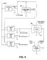
- FIG. 5 shows an example of a practical application of the tracking method of the present invention as implemented in a practical design.
- DC-DC converters Four isolated DC-DC converters are used to provide power to the system. Three of these converters (3.3V and 2X2.5V outputs) are standard modules which operate in the input voltage range 36 to 75V. The fourth one, the 5V output, operates over a wide input range 18 to 75V, and is designed to start faster than the remaining three major converters.
- the main function of the +5V converter is to provide early supply voltage for the monitoring circuit 60 which, via On/Off pins controls the major converters. As shown, the early 5V converter is not part of the On/Off loop.
- the rail tracking in the system is required between the 3.3V and 2.5V rails and between the 3.3V Vi/o and 2.0V Vcore for the dual power IC. Tracking between high current rails (3.3V/60A and 2.5V/20A) has been provided using the linear series pass regulator circuit as illustrated in Figure 3 .
- the tracking method according to the preferred embodiment of Figure 4 is used for providing tracking between the 3.3V and 2.0V rail for the dual power IC.
- the 3.3V to 2.0V module is a non-isolated, DC-DC switch mode power supply.
- the pin to supply the supply voltage to the pulse width modulator is isolated in order that voltage from the early 5V supply can be connected directly to the pulse width modulator.
Landscapes
- Engineering & Computer Science (AREA)
- Power Engineering (AREA)
- Physics & Mathematics (AREA)
- Electromagnetism (AREA)
- General Physics & Mathematics (AREA)
- Radar, Positioning & Navigation (AREA)
- Automation & Control Theory (AREA)
- Dc-Dc Converters (AREA)
Claims (9)
- Méthode de cheminement de rails pour produire deux niveaux de tension sur des premier et deuxième rails de tension sur un circuit intégré (IC), comprenant :la fourniture d'une première tension sur ledit premier rail de tension ;la fourniture de ladite première tension sur un régulateur de tension (14) ayant des moyens de conversion (50) pour dériver une deuxième tension pour ledit deuxième rail de tension ; etla fourniture d'une tension d'alimentation sur lesdits moyens de conversion (50) avant l'étape de fourniture de ladite première tension sur ledit régulateur de tension (14).
- Procédé selon la revendication 1, dans lequel lesdits moyens de conversion (50) utilisent un modulateur d'impulsions en durée (PWM) pour dériver ladite deuxième tension de ladite première tension.
- Système pour produire un cheminement de rails pour deux niveaux de tension sur des premier et deuxième rails de tension sur un circuit intégré (IC), comprenant :des premiers moyens de tension, pour appliquer un premier niveau de tension sur ledit premier rail de tension ;un régulateur de tension (14) ayant des moyens pour recevoir ledit premier niveau de tension ; des moyens de conversion (50) dans ledit régulateur de tension pour dériver un deuxième niveau de tension pour ledit deuxième rail de tension à partir dudit premier niveau de tension ;des moyens de tension d'alimentation pour appliquer une tension d'alimentation auxdits moyens de conversion (50) ; et des moyens contrôlant lesdits moyens d'alimentation pour appliquer ladite tension d'alimentation auxdits moyens de conversion (50) avant que ladite première tension soit appliquée audit régulateur de tension (14).
- Système selon la revendication 3, dans lequel lesdits moyens de conversion (50) incluent un modulateur d'impulsions en durée (PWM).
- Système selon la revendication 4, comprenant en outre une diode de cheminement arrière (54) entre ledit deuxième rail de tension et ledit premier rail de tension.
- Système selon la revendication 5, dans lequel ledit premier niveau de tension applique des fonctions d'entrée/sortie sur ledit IC et ledit deuxième niveau de tension alimente un coeur de processeur sur ledit IC.
- Système selon la revendication 6, dans lequel ladite tension d'alimentation est appliquée par une alimentation en mode continu-continu.
- Système selon la revendication 7, dans lequel ledit IC exécute de multiples fonctions nécessitant des niveaux doubles de tension de fonctionnement, ledit régulateur de tension (14) emploie un convertisseur de commutation pour recevoir ledit premier niveau de tension et en dériver un deuxième niveau de tension pour ledit IC, et dans lequel ledit système comprend :une deuxième alimentation en mode continu-continu pour appliquer une tension de fonctionnement audit convertisseur de commutation ; moyennant quoi ladite deuxième alimentation en continu-continu applique ladite tension de fonctionnement audit convertisseur de commutation de telle sorte que ledit convertisseur soit opérationnel avant que ledit premier niveau de tension pour dériver ledit deuxième niveau de tension soit appliqué au régulateur de tension (14).
- Système selon la revendication 8, dans lequel ledit régulateur de tension (14) comprend une connexion séparée (52) pour recevoir ladite tension d'alimentation.
Applications Claiming Priority (2)
| Application Number | Priority Date | Filing Date | Title |
|---|---|---|---|
| US456392 | 1989-12-26 | ||
| US09/456,392 US6172490B1 (en) | 1999-12-08 | 1999-12-08 | Precise rail tracking method for powering dual voltage integrated circuits |
Publications (3)
| Publication Number | Publication Date |
|---|---|
| EP1107095A2 EP1107095A2 (fr) | 2001-06-13 |
| EP1107095A3 EP1107095A3 (fr) | 2008-12-03 |
| EP1107095B1 true EP1107095B1 (fr) | 2011-04-06 |
Family
ID=23812570
Family Applications (1)
| Application Number | Title | Priority Date | Filing Date |
|---|---|---|---|
| EP00310831A Expired - Lifetime EP1107095B1 (fr) | 1999-12-08 | 2000-12-06 | Procédé d'alimentation de circuits intégrés à double tension |
Country Status (3)
| Country | Link |
|---|---|
| US (2) | US6172490B1 (fr) |
| EP (1) | EP1107095B1 (fr) |
| DE (1) | DE60045811D1 (fr) |
Families Citing this family (13)
| Publication number | Priority date | Publication date | Assignee | Title |
|---|---|---|---|---|
| EP1157046B1 (fr) * | 1999-12-28 | 2005-12-07 | Basell Polyolefine GmbH | Processus de preparation de polymeres d'ethylene |
| US20040145358A1 (en) * | 2001-04-19 | 2004-07-29 | Rogers Terrence Edwards | Method and apparatus for minimizing power dissipation in series connected voltage regulators |
| US6948079B2 (en) * | 2001-12-26 | 2005-09-20 | Intel Corporation | Method and apparatus for providing supply voltages for a processor |
| US6661211B1 (en) | 2002-06-25 | 2003-12-09 | Alcatel Canada Inc. | Quick-start DC-DC converter circuit and method |
| US6917123B2 (en) * | 2002-09-25 | 2005-07-12 | Dell Products L.P. | Synchronized power-up for multiple voltage system |
| US7498874B1 (en) | 2006-08-03 | 2009-03-03 | National Semiconductor Corporation | Glitch-free start-up with a tracking pin |
| US7705574B2 (en) * | 2008-06-13 | 2010-04-27 | Hamilton Sundstrand Corporation | Remote power controller with power sharing circuit |
| KR20120100238A (ko) * | 2011-03-03 | 2012-09-12 | 삼성전자주식회사 | 반도체 장치, 이의 동작 방법, 및 상기 반도체 장치를 포함하는 반도체 시스템 |
| KR101266834B1 (ko) * | 2012-04-24 | 2013-05-27 | 엘에스산전 주식회사 | 디지털 보호계전기 |
| US9077514B1 (en) | 2014-01-28 | 2015-07-07 | Altera Corporation | Methods and structures for compensating and tracking process, voltage and temperature variations |
| US9559642B2 (en) | 2015-01-02 | 2017-01-31 | Logitech Europe, S.A. | Audio delivery system having an improved efficiency and extended operation time between recharges or battery replacements |
| JP6466761B2 (ja) * | 2015-03-31 | 2019-02-06 | ラピスセミコンダクタ株式会社 | 半導体装置、及び電源供給方法 |
| CN111079371B (zh) * | 2019-12-19 | 2024-03-15 | 武汉新芯集成电路制造有限公司 | 双电源标准单元、双电源标准单元库及集成电路设计方法 |
Family Cites Families (11)
| Publication number | Priority date | Publication date | Assignee | Title |
|---|---|---|---|---|
| JPS6115620Y2 (fr) * | 1976-03-02 | 1986-05-15 | ||
| US4472687A (en) * | 1980-12-24 | 1984-09-18 | Tokyo Shibaura Denki Kabushiki Kaisha | Audio power amplifier for supplying electric power to a load by switching of power supply voltage |
| SE467331B (sv) * | 1990-10-26 | 1992-06-29 | Andersson & Baevholm Lab | Audio-effektfoerstaerkare med pulsbreddsmodulering samt ett audio-effektsteg |
| US5550729A (en) * | 1994-06-09 | 1996-08-27 | Digital Equipment Corporation | Power sequencing control |
| US5606289A (en) * | 1994-06-22 | 1997-02-25 | Carver Corporation | Audio frequency power amplifiers with actively damped filter |
| US5543753A (en) * | 1994-06-22 | 1996-08-06 | Carver Corporation | Audio frequency power amplifiers with actively damped filter |
| ATE211834T1 (de) * | 1994-10-07 | 2002-01-15 | Elonex Technologies Inc | Verbesserter spannungsregler für ein cpu mit variabler spannung |
| US5898340A (en) * | 1996-11-20 | 1999-04-27 | Chatterjee; Manjirnath A. | High power efficiency audio amplifier with digital audio and volume inputs |
| US5864225A (en) * | 1997-06-04 | 1999-01-26 | Fairchild Semiconductor Corporation | Dual adjustable voltage regulators |
| KR100321976B1 (ko) * | 1997-12-29 | 2002-05-13 | 윤종용 | 인텔프로세서를위한오류허용전압조절모듈회로 |
| US6011382A (en) * | 1998-10-01 | 2000-01-04 | Toko, Inc. | Circuit and method for directly regulating the output voltage of an electroluminescent lamp driver |
-
1999
- 1999-12-08 US US09/456,392 patent/US6172490B1/en not_active Expired - Lifetime
-
2000
- 2000-12-05 US US09/729,174 patent/US6288523B2/en not_active Expired - Lifetime
- 2000-12-06 DE DE60045811T patent/DE60045811D1/de not_active Expired - Lifetime
- 2000-12-06 EP EP00310831A patent/EP1107095B1/fr not_active Expired - Lifetime
Also Published As
| Publication number | Publication date |
|---|---|
| EP1107095A2 (fr) | 2001-06-13 |
| DE60045811D1 (de) | 2011-05-19 |
| US6288523B2 (en) | 2001-09-11 |
| EP1107095A3 (fr) | 2008-12-03 |
| US20010003417A1 (en) | 2001-06-14 |
| US6172490B1 (en) | 2001-01-09 |
Similar Documents
| Publication | Publication Date | Title |
|---|---|---|
| US6574124B2 (en) | Plural power converters with individual conditioned error signals shared on a current sharing bus | |
| US8432146B2 (en) | Correcting pre-bias during turn-on of switching power regulators | |
| US6462525B1 (en) | Polyphase PWM converter with high efficiency at light loads | |
| US6469478B1 (en) | Multiple output power supply including one regulated converter and at least one semi-regulated converter | |
| US6346798B1 (en) | Single wire current sharing control technique for the parallel/redundant operation of a plurality of PWM converters | |
| US8576589B2 (en) | Switch state controller with a sense current generated operating voltage | |
| US6768658B2 (en) | DC-DC power supply with at least two paralleled converters and current share method for same | |
| US20080164759A1 (en) | Redundant power supply architecture with voltage level range based load switching | |
| JP4295120B2 (ja) | 並列接続された複数のスイッチング電源を備えた電力供給装置 | |
| EP1107095B1 (fr) | Procédé d'alimentation de circuits intégrés à double tension | |
| US7738227B2 (en) | Control system and method with constant maximum current for power converter protection | |
| EP2984745B1 (fr) | Commande de chute de tension au sein d'une alimentation à découpage commandé en tension | |
| US20030035260A1 (en) | Integrated circuit for generating a plurality of direct current (DC) output voltages | |
| EP3269029B1 (fr) | Utilisation d'un commutateur de puissance pmos dans une combinaison de régulateur linéaire et de commutation | |
| WO2006083347A2 (fr) | Procede de statisme compense permettant de mettre en parallele des alimentations (procede de statisme c) | |
| US11329556B1 (en) | Multi-input single output power system and operating method thereof | |
| US5861738A (en) | DC to DC converter with a single-fault tolerant clamp | |
| US6424545B2 (en) | Efficient, dual-source, wide-input range, isolated DC-DC converter with effective current limit | |
| CN101034850B (zh) | Dc-dc转换器及其控制电路和控制方法,以及电源单元 | |
| US11159088B2 (en) | Dual path and mode start-up circuit | |
| US7692939B2 (en) | Control circuit | |
| WO2007032755A1 (fr) | Procede destine a former un circuit de detection de courant et structure associee | |
| Kim et al. | Start-up control to prevent overcurrent during hot swap in paralleled DC–DC converters | |
| JP2803151B2 (ja) | 電源装置 | |
| US20260121540A1 (en) | Status report of power stage circuit for multiphase voltage regulator |
Legal Events
| Date | Code | Title | Description |
|---|---|---|---|
| PUAI | Public reference made under article 153(3) epc to a published international application that has entered the european phase |
Free format text: ORIGINAL CODE: 0009012 |
|
| AK | Designated contracting states |
Kind code of ref document: A2 Designated state(s): AT BE CH CY DE DK ES FI FR GB GR IE IT LI LU MC NL PT SE TR |
|
| AX | Request for extension of the european patent |
Free format text: AL;LT;LV;MK;RO;SI |
|
| PUAL | Search report despatched |
Free format text: ORIGINAL CODE: 0009013 |
|
| AK | Designated contracting states |
Kind code of ref document: A3 Designated state(s): AT BE CH CY DE DK ES FI FR GB GR IE IT LI LU MC NL PT SE TR |
|
| AX | Request for extension of the european patent |
Extension state: AL LT LV MK RO SI |
|
| 17P | Request for examination filed |
Effective date: 20090603 |
|
| AKX | Designation fees paid |
Designated state(s): DE ES FR GB IT |
|
| 17Q | First examination report despatched |
Effective date: 20090805 |
|
| GRAP | Despatch of communication of intention to grant a patent |
Free format text: ORIGINAL CODE: EPIDOSNIGR1 |
|
| GRAS | Grant fee paid |
Free format text: ORIGINAL CODE: EPIDOSNIGR3 |
|
| GRAA | (expected) grant |
Free format text: ORIGINAL CODE: 0009210 |
|
| AK | Designated contracting states |
Kind code of ref document: B1 Designated state(s): DE ES FR GB IT |
|
| REG | Reference to a national code |
Ref country code: GB Ref legal event code: FG4D |
|
| REF | Corresponds to: |
Ref document number: 60045811 Country of ref document: DE Date of ref document: 20110519 Kind code of ref document: P |
|
| REG | Reference to a national code |
Ref country code: DE Ref legal event code: R096 Ref document number: 60045811 Country of ref document: DE Effective date: 20110519 |
|
| RAP2 | Party data changed (patent owner data changed or rights of a patent transferred) |
Owner name: ALCATEL LUCENT |
|
| PG25 | Lapsed in a contracting state [announced via postgrant information from national office to epo] |
Ref country code: ES Free format text: LAPSE BECAUSE OF FAILURE TO SUBMIT A TRANSLATION OF THE DESCRIPTION OR TO PAY THE FEE WITHIN THE PRESCRIBED TIME-LIMIT Effective date: 20110717 |
|
| PLBE | No opposition filed within time limit |
Free format text: ORIGINAL CODE: 0009261 |
|
| STAA | Information on the status of an ep patent application or granted ep patent |
Free format text: STATUS: NO OPPOSITION FILED WITHIN TIME LIMIT |
|
| 26N | No opposition filed |
Effective date: 20120110 |
|
| REG | Reference to a national code |
Ref country code: DE Ref legal event code: R097 Ref document number: 60045811 Country of ref document: DE Effective date: 20120110 |
|
| REG | Reference to a national code |
Ref country code: FR Ref legal event code: GC Effective date: 20131018 |
|
| PG25 | Lapsed in a contracting state [announced via postgrant information from national office to epo] |
Ref country code: IT Free format text: LAPSE BECAUSE OF FAILURE TO SUBMIT A TRANSLATION OF THE DESCRIPTION OR TO PAY THE FEE WITHIN THE PRESCRIBED TIME-LIMIT Effective date: 20110406 |
|
| REG | Reference to a national code |
Ref country code: FR Ref legal event code: RG Effective date: 20141016 |
|
| REG | Reference to a national code |
Ref country code: FR Ref legal event code: PLFP Year of fee payment: 16 |
|
| REG | Reference to a national code |
Ref country code: FR Ref legal event code: PLFP Year of fee payment: 17 |
|
| REG | Reference to a national code |
Ref country code: FR Ref legal event code: PLFP Year of fee payment: 18 |
|
| PGFP | Annual fee paid to national office [announced via postgrant information from national office to epo] |
Ref country code: DE Payment date: 20181120 Year of fee payment: 19 |
|
| PGFP | Annual fee paid to national office [announced via postgrant information from national office to epo] |
Ref country code: GB Payment date: 20181205 Year of fee payment: 19 Ref country code: FR Payment date: 20181120 Year of fee payment: 19 |
|
| REG | Reference to a national code |
Ref country code: DE Ref legal event code: R119 Ref document number: 60045811 Country of ref document: DE |
|
| GBPC | Gb: european patent ceased through non-payment of renewal fee |
Effective date: 20191206 |
|
| PG25 | Lapsed in a contracting state [announced via postgrant information from national office to epo] |
Ref country code: GB Free format text: LAPSE BECAUSE OF NON-PAYMENT OF DUE FEES Effective date: 20191206 Ref country code: FR Free format text: LAPSE BECAUSE OF NON-PAYMENT OF DUE FEES Effective date: 20191231 Ref country code: DE Free format text: LAPSE BECAUSE OF NON-PAYMENT OF DUE FEES Effective date: 20200701 |