BACKGROUND OF THE INVENTION
Field of Invention
-
The present invention relates to an organic
electroluminescence element (hereinafter sometimes called
the "organic EL element" or "EL element") and the
manufacturing method thereof.
-
Particularly, the present invention relates to an
organic EL element which has a large light-emitting area
suited for noncommercial and industrial-use display devices
(liquid displays and the like) and which can be used for
various electrode materials and to the manufacturing method
that can obtain such organic EL elements efficiently.
Description of Related Art
-
One example of the conventional organic EL element is
disclosed in, for example, JP-A-3-262170. Referring now to
Fig. 13, the configuration is explained. An organic layer
202 is interposed between a first electrode 201 and a
second electrode 203 and at least the first layer 201 is
composed with inorganic semiconductor material, namely,
monocrystal semiconductor materials such as GaP, GaAlAs,
GaAsP, ZnS, and the like.
-
When the first electrode 201 is of an n-type
semiconductor, the joined surface of the first electrode
201 and the organic layer 202 is made by electron injection
joining from the first electrode 201 to the organic layer
202, that is, electron injection is achieved by tunnel
effects.
-
In addition, when the first electrode 201 is of the
p-type semiconductor, the joined surface of the first
electrode 201 and the organic layer 202 is made by hole
injection joining from the first electrode 201 to the
organic layer 202, where the hole injection is carried out
by the tunnel effects.
-
Incidentally, in Fig. 13, the first electrode 201 is
represented by symbol "P", the organic layer 202 is
represented by symbol "O", and the second electrode 203 is
represented by symbol "M".
-
However, the organic EL element disclosed in JP-A-3-262170
has the first electrode 201 which is opposed to the
second electrode 203 as shown in Fig. 13, and EL emission
light is taken out from either of the electrodes 201 or
203. Consequently, with regard to the light transmittance
of the electrode, there are problems in that the electrode
material is limited to transparent material, such as indium
tin oxide (ITO) or the blue light is difficult to be
effectively obtained from the electrodes 201, 203.
-
Furthermore, the electrodes 201, 203 are composed
with monocrystal semiconductor material in these organic EL
elements, there is a big restriction in manufacturing. More
concretely, since making such monocrystal semiconductor
material is not easy, it is difficult to produce an organic
EL element with a large area.
-
Consequently, in JP-A-8-180974 and JP-A-11-31590, or
WO97/34447, as shown in Fig. 14, an auxiliary electrode 213
is provided in part of the electrode 212 and the low
resistance is obtained as a whole electrode.
-
However, as electrodes are opposed each other in all
inorganic EL electrodes or organic EL elements to transmit
the light effectively, consequently, the transparent
materials such as ITO must be used for the electrode.
-
Therefore, the inventors of the present invention
diligently have investigated the above-mentioned problems
and found out that the conventional problems could be
solved by installing an organic light-emitting medium
between either an anodic or cathodic electrode (first
electrode) and a semiconductor layer comprising non-monocrystal
material as well as electrically connecting the
other electrode (second electrode) to the edge section of
the semiconductor layer.
-
Accordingly, it is an object of the present invention
to provide an organic EL element that can be used for a
wide variety of electrode materials and that has a large
area, as well as to provide a manufacturing method that can
obtain such organic EL element efficiently.
SUMMARY OF THE INVENTION
-
- [1] One of the embodiments according to the present
invention relates to an organic EL element comprising an
anode, a semiconductor layer, an organic light-emitting
medium, and a cathode,
characterized in that an organic light-emitting
medium is located between the first electrode and the
semiconductor layer comprising the non-monocrystal material
and the second electrode is electrically connected to the
edge section of the semiconductor layer when either one of
the anode or cathode is designated to the first electrode
and the other electrode to the second electrode.
Because the first electrode and the second electrode
are not substantially opposite to each other by configuring
such organic EL element, there is no restriction to the
materials used for these electrodes because the
consideration of the luminous taken out to the outside is
not needed. Consequently, low-resistance opaque materials
can be used for each electrode.In addition, because the electrode is made from the
non-monocrystal materials, a large-area organic EL element
can be also obtained.Furthermore, because the second electrode does not
serve as a barrier material even when the light is taken
out from the semiconductor layer to the outside, the light
energy volume that is taken outside can be increased.
- [2] In configuring the organic EL element according to
the present invention, it is preferable that the second
electrode is electrically connected to the extended section
extended in the horizontal direction from the edge section
of the semiconductor layer.
By configuring in this way, the electrically
connected section between the second electrode and the
semiconductor layer can be made into a big area and can
stabilize the connection resistance, and can prevent short-circuit
between the second electrode and the organic light-emitting
medium.By the way, as described later, in the horizontally
extended section of the semiconductor layer, the second
electrode may be formed at the position that achieves the
same level as that of the organic light-emitting medium, or
a recessed section is formed at the horizontally extended
section on which the second electrode may be formed.
- [3] In configuring the organic EL element according to
the present invention, it is preferable for the second
electrode to be electrically connected to two or more edge
sections of the semiconductor layer.
By configuring in this way, it is possible to make
the electrically connected section between the second
electrode and the semiconductor layer into a large area,
and even if one electrically connected section fails,
conductivity is able to be secured by other electrically
connected sections.
- [4] In configuring the organic EL element according to
the present invention, it is preferable for the second
electrode to be made in patterns of lattices or combs.
By configuring in this way, the organic light-emitting
medium is allowed to emit light uniformly and the
light energy which is taken outside is increased at the
same time.
- [5] In addition, in configuring the organic EL element
according to the present invention, it is preferable that
the non-monocrystal material is one of the charcogenide
materials selected from a group consisting of ZnS, ZnSe,
CdS, CdTe, ZnTe, MgS, MgSe, ZnSSe, ZnMgSSe, ZnCdSSe, and
ZnTeSe.
By configuring the semiconductor layer with these
non-monocrystal materials, it is able to easily achieve a
large area. In addition, if the semiconductor layer
comprises these non-monocrystal materials, the light energy
that can be taken out to the outside may be increased.
- [6] In addition, in configuring the organic EL element
according to the present invention, it is preferable that
the non-monocrystal material is at least one of the metal
oxide non-degenerate semiconductors selected from a group
consisting of Al, Sn, Zn, In, Cd, Mg, and Si.
By configuring the semiconductor layer with these
non-monocrystal materials, large area can be easily
obtained. In addition, if the semiconductor layer comprises
these non-monocrystal materials, the light energy that can
be taken out to the outside may be increased.
- [7] In configuring the organic EL element according to
the present invention, it is preferable that the non-monocrystal
material is either amorphous carbon or diamond-like
carbon.
By configuring the semiconductor layer with this kind
of non-monocrystal materials, a large area can be easily
obtained.
- [8] In configuring the organic EL element according to
the present invention, it is preferable that the non-monocrystal
material is an conductive conjugate polymer, an
oxidizing agent added polymer, an reducing agent added
polymer, an oxidizing agent added low-molecular weight
compound, or a reducing agent added low-molecular weight
compound.
By configuring in this way, an increased area may be
easily achieved and a semiconductor layer with excellent
surface smoothness may be formed, and element defects can
be reduced.
- [9] In configuring the organic EL element according to
the present invention, it is preferable that the band gap
of the semiconductor layer is held to 2.7 eV or higher.
Because by configuring in this way, it is possible to
improve the transparency of the semiconductor layer, the EL
light energy taken out to the outside can be increased.
- [10] In configuring the organic EL element according to
the present invention, it is preferable that the thickness
of the semiconductor layer is held within 1-700 nm.
By configuring in this way, the specified intensity
may be obtained and at the same time, the transparency of
the semiconductor layer can be improved, and the EL light
energy taken out to the outside can be increased.
- [11] In configuring the organic EL element according to
the present invention, it is preferable that the specific
resistance of the semiconductor layer is held within the
range of 1 x 10⁻³ to 1 x 10⁴Ω · cm.
By configuring in this way, the driving voltage of
the organic EL element can be lowered further and at the
same time, the luminance in the light-emitting surface can
be homogenized.
- [12] In configuring the organic EL element according to
the present invention, it is preferable that the electric
charge concentration of the semiconductor layer is held
within the range of 1 x 10¹² to 1 x 1020 cm-3.
By configuring in this way, the driving voltage of
the organic EL element can be lowered and at the same time,
the quenching under the exciting condition in the organic
light emitting medium may be prevented.
- [13] In configuring the organic EL element according to
the present invention, it is preferable that the light
transmittance of the semiconductor layer is held to 10% or
more.
By configuring in this way, the EL light energy taken
out to the outside can be increased.The light transmittance of the semiconductor layer
has effects on the wavelength of the transmitting light,
and in general, even when the light transmittance is about
10% but when it is the light with smaller energy
(wavelength) than the band gap of the semiconductor layer,
it is known that the light transmittance of, for example,
greater than 80% can be easily obtained.
- [14] In configuring the organic EL element according to
the present invention, it is preferable that an electric
insulation section is located between the second electrode
and the organic light-emitting medium.
By configuring in this way, short-circuits between
the second electrode and the organic light-emitting medium
and cross-talk of the display screen can be definitely
prevented.
- [15] In configuring the organic EL element according to
the present invention, it is preferable to configure in
such a manner that the EL light emitting is taken out from
the semiconductor layer to the outside.
By configuring in this way, it becomes possible to
use various electrode materials in the first electrode.
- [16] In configuring the organic EL element according to
the present invention, it is preferable that the conductive
layer is interposed between the second electrode and the
semiconductor layer.
By configuring in this way, it becomes possible to
lower the connection resistance between the second
electrode and the semiconductor layer, and furthermore it
becomes possible to easily inject electrons and holes.
- [17] In configuring the organic EL element according to
the present invention, it is preferable that an auxiliary
electrode is provided for the second electrode.
By configuring in this way, it becomes possible to
further lower the resistance of the second electrode and to
drive the organic EL element at low voltage.
- [18] The other embodiment of the present embodiment is a
manufacturing method of the organic EL element including
the anode, semiconductor layer, organic light-emitting
medium, and the cathode, comprising
- a step for forming the second electrode,
- a step for forming a semiconductor layer at the
position where the second electrode is able to be
electrically connected to the edge section of the
semiconductor layer using the non-monocrystal material,
- a step for forming the organic light-emitting medium,
- a step for forming the first electrode,
- when either of the anode or cathode is called the
first electrode and the other electrode the second
electrode.
- [19] In addition, it is preferable to include a step for
patterning in the step for forming the second electrode
when the manufacturing method of the organic EL element
according to the present invention is implemented.
By implementing in this way, the organic EL element
is able to allow the organic EL element to emit the light
in the specified pattern, and when a plurality of patterns
are possessed, each of them can be emitted electrically
independently.By further embodying in this way, the contact area
between the second electrode and the semiconductor layer
can be increased, and the low-voltage drive of the organic
EL element is ensured.
- [20] In implementing the method for manufacturing the
organic EL element according to the present invention, it
is preferable to include a step for forming the electric
insulation film for covering the second electrode, or a
step for forming the non-injection type semiconductor layer
or metal layer.
-
-
By configuring in this way, the second electrode may
be mechanically and chemically protected, and furthermore,
short-circuits can be prevented and the injection of holes
or electrons from the second electrode can be prevented.
BRIEF DESCRIPTION OF THE DRAWINGS
-
Fig. 1 is a cross-sectional view describing the
construction of the organic EL element in the first
embodiment.
-
Fig. 2 is a cross-sectional view for describing the
construction of the organic EL element in the modified
example of the first embodiment (No. 1).
-
Fig. 3 is a cross-sectional view for describing the
construction of the organic EL element in the modified
example of the first embodiment (No. 2).
-
Fig. 4 is a cross-sectional view for describing the
construction of the organic EL element in the modified
example of the first embodiment (No. 3).
-
Fig. 5 is a cross-sectional view for describing the
construction of the organic EL element in the modified
example of the first embodiment (No. 4).
-
Fig. 6 is a cross-sectional view for describing the
construction of the organic EL element in the modified
example of the first embodiment (No. 5).
-
Fig. 7 is a cross-sectional view for describing the
construction of the organic EL element in the modified
example of the first embodiment (No. 6).
-
Fig. 8 is a cross-sectional view for describing the
construction of the organic EL element in the modified
example of the first embodiment (No. 7).
-
Fig. 9 is a drawing for describing the connection
structure between the second electrode and the
semiconductor layer (No. 1).
-
Fig. 10 is a drawing for describing the connection
structure between the second electrode and the
semiconductor layer (No. 2).
-
Fig. 11 is a drawing for describing the connection
structure between the second electrode and the
semiconductor layer (No. 3).
-
Fig. 12 is a cross-sectional view for describing a
manufacturing method related to the second embodiment.
-
Fig. 13 is a cross-sectional view for describing the
structure of a conventional organic EL element (No. 1).
-
Fig. 14 is a cross-sectional view for describing the
structure of a conventional organic EL element (No. 2).
DETAILED DESCRIPTION OF THE PREFERRED EMBODIMENT
-
Referring now to drawings, embodiments according to
the present invention will be described specifically as
follows. The drawings referred here only generally show the
size, profile, and arrangement relations of each component
member to understand the present invention. Consequently,
this invention should not be limited to the illustrated
examples. In the drawings, there are cases in that hatching
that indicates the cross section may be omitted.
[First Embodiment]
-
Referring now to Fig. 1, the first embodiment
according to the present invention will be described. Fig.
1 is a cross-sectional view of an organic EL element in the
first embodiment, wherein on the support substrate 15, a
semiconductor layer 14 comprising non-monocrystal material,
an organic light-emitting medium 12, and a cathode (first
cathode) 10 are formed successively. To the extension 18
extended in the horizontal section from the edge section 17
of the semiconductor layer 14, the anode (second electrode)
16 is electrically connected.
-
Consequently, as the light may be taken out from the
semiconductor layer 14 to the outside by configuring in
this way, the light energy (or light intensity) can be
increased. In addition, since the anode (second electrode)
16 and the cathode (first electrode) are not practically
opposite to each other, a wide variety of electrode
materials may be used and the electrical connection to the
outside is facilitated. In addition, since the
semiconductor layer 14 is composed with the non-monocrystal
material, a semiconductor layer 14 of a large area may be
formed. Consequently, because it is possible to form the
organic light-emitting medium 12, and the like on the
semiconductor layer 14, as a result, an organic EL element
100 of a large area can be configured.
(1) Organic light-emitting medium
(i) Composing material
-
The organic light-emitting material used for the
composing material of the organic light-emitting layer
preferably provides the following three functions in
combination.
- (a) Electric charge injection function: A function
for injecting electrons from the cathode or the electron
injection layer while holes are able to be injected from
the anode or hole injecting layer when the electrical field
is applied.
- (b) Transportation function: A function for moving
injected holes and electrons by the force of the electrical
field.
- (c) Light-emitting function: A function for providing
a field for re-combining electrons with holes and for
allowing these to emit light.
-
-
However, it is not always necessary for the organic-light
emitting material to have all of the functions of (a)
to (c) above, and for example, there are suitable ones as
organic light-emitting materials of those whose hole
injection transportability is far better than the electron
injection transportability. Consequently, the materials
that promote the electron transportation in the organic
light-emitting layer and the electrons can recombine with
holes in the vicinity of the center of the organic light-emitting
layer can be suitably used.
-
Now, in order to improve the recombination
capabilities in the organic light-emitting layer, the
electron mobility of the organic light-emitting material is
preferably set to 1 x 10⁻⁷ cm2/V·s or higher. The reason is
when it becomes less than 1 x 10⁻⁷ cm2/V·s, the high-speed
response in the organic EL element may become difficult or
the light-emitting luminance may be lowered.
-
Consequently, the electron mobility of the organic
light-emitting material is preferably set to a value within
the range of 1.1 x 10⁻⁷ to 2 x 10⁻³ cm2/V·s and is more
suitably set to a value within the range of 1.2 x 10⁻⁷ to 1
x 10-3 cm2/V·s.
-
In addition, it is preferable that the electron
mobility is smaller than the hole mobility of the organic
light-emitting material in the organic light-emitting
layer. This is because if the electron mobility is reversal
to this, the organic light-emitting material used for the
organic light-emitting layer may be excessively limited and
the light-emitting luminance may be lowered.
-
On the other hand, the electron mobility of the
organic light-emitting material is preferably greater than
1/1000 times as much as the hole mobility. This is because
when the electron mobility becomes excessively small, it
becomes difficult for the electron to recombine with the
hole in the vicinity of the center of the organic light-emitting
layer, and as a result, the light-emitting
luminance may be lowered.
-
Consequently, the hole mobility (µh) and the electron
mobility (µe) of the organic light-emitting material in the
organic light-emitting layer preferably satisfy the
relation of µh/2 > µe > µh/500, and more suitably satisfy the
relation of µh/3 >µe> µh/100.
-
In the first embodiment, it is preferable to use
aromatic cyclic compounds with a styryl group expressed by
the following equations (1) to (3).
-
The use of this kind of aromatic cyclic compounds
with a styryl group can easily satisfy the conditions of
electron mobility and hole mobility of the organic light-emitting
material in the organic light-emitting layer
described above.
-
"In the general formula (1), Ar
1 denotes the aromatic
group with the number of carbons ranging from 6 to 50, Ar
2,
Ar
3, and Ar
4 are aromatic groups with the number of carbons
ranging from 6 to 50 or a hydrogen atom, at least one of
Ar
1, Ar
2, Ar
3, and Ar
4 is the aromatic group, and the number
of condensation n is an integer from 1 to 6."
-
"In the general formula (2), Ar
5 denotes the aromatic
group with the number of carbons ranging from 6 to 50, Ar6
and Ar7 are a hydrogen atom aromatic groups with the number
of carbons ranging from 6 to 50 which may be replaced, and
the number of condensation m is an integer from 1 to 6."
-
"In the general formula (3), Ar8 and Ar14 denote the
aromatic group with the number of carbons ranging from 6 to
50, Ar9 through Ar13 are a hydrogen atom or aromatic groups
with the number of carbons ranging from 6 to 50 which may
be replaced, and the numbers of condensation p, q, r, s are
0 or 1, respectively."
-
Now, for the aromatic group, examples of allyl group
with the number of nuclear atoms ranging from 5 to 40
include phenyl, naphthyl, anthranil, phenanthryl, pyrenyl,
coronyl, biphenyl, terphenyl, pyrrolyl, furanyl,
thiophenyl, benzothiophenyl, oxadiazoril,
diphenylanthranil, indolyl, carbazolyl, pyridyl,
benzoquinolil, dibenzochrysenilene, and the like.
-
Examples of preferable allylene group with the number
of nuclear atoms ranging from 5 to 40 include phenylene,
naphthylene, anthranilene, phenanthrylene, pyrenylene,
coronylene, bipheylene, terphenylene, pyrrolylene,
furanylene, thiophenylene, benzothiopheylene,
oxadiazorilene, diphenylanthranilene, indolylene,
carbanzolylene, pyridylene, benzoquinolilene,
dibenzochryenilene, and the like.
-
These aromatic groups may be further replaced by
different substitutes. Examples of preferable substitutes
include alkyl group with the number of carbons from 1 to 6
(or an ethyl group, a methyl group, an i-propyl group, a n-propyl
group, a s-butyl group, a t-butyl group, a pentyl
group, a hexyl group, a cyclohexyl group, and the like), an
alkoxy group with the number of carbons from 1 to 6 (or an
ethoxyl group, a methoxyl group, an i-propoxy group, a n-propoxy
group, a s-butoxy group, a t-butoxy group, a
pentoxy group, a hexyloxy group, a cyclopentoxy group, a
cyclohexyloxy group, and the like), an aryl group radical
of the number of nuclear atoms of 5 to 40, an amino group
substituted with an aryl radical with the number of nuclear
atoms of 5 to 40, an ester group with an aryl radical of
number of nuclear atoms ranging from 5 to 40, an ester
group with an alkyl group of number of carbons of 1 to 6, a
cyano group, a nitro group, and a halogen atom.
-
It is also preferable to use benzothiazole-based
compounds, benzoimidazole-based compounds, benzooxyazole-based
compounds, and other fluorescent brighteners
compounds, styrylbenzene-based compounds, metal complexes
with 8-quinolinol derivative as a ligand in combination.
-
It is also suitable to use the material in
combination, in which the organic light-emitting material
of distyryl allylene skeleton, for example, 4,4'-bis(2,2-diphenylvinyl)
biphenyl, and the like is used as a host and
the strong fluorescent pigments from blue to red, for
example, coumarin-based fluorescent pigments or pigments
similar to the host, is doped in the host.
(ii) Forming method
-
Next discussion will be made on the method for
forming the organic light-emitting layer. This kind of
forming method is not particularly limited, but, for
example, a vacuum deposition method, a spin-coating method,
a casting method, a LB (Langmuir-Blodgett) method, a
sputtering method, and the like may be used. For example,
in the case of forming by the vacuum deposition method, it
is preferable to adopt the conditions of 50-450°C for
deposition temperature, in an inert gas, 1 x 10⁻⁷ to 1 x 10⁻³
Pa for vacuum, 0.01 to 50 nm/sec. for film forming rate,
and 50 to 300°C for substrate temperature.
In addition, it is possible to form the organic
light-emitting layer by dissolving binder resins and
organic light-emitting materials in a solvent to achieve
the solution condition, and then forming the solution into
thin film by a spin-coating method, and the like. Now, the
preferable binder is a transparent resin, and examples of
the particularly preferable binder include polycarbonate,
polystyrene, polyolefin, polyimide, polysulfone, and the
like.
(iii) Film thickness
-
There is no particular limitation to the film
thickness of an organic light-emitting layer, and any film
thickness may be chosen as required in accordance with
conditions, but specifically, it is preferable that the
film thickness is within the range of 5 nm to 5 µm. This is
because when the film thickness of the organic light-emitting
layer becomes less than 5 nm, the light-emitting
luminance or durability may be lowered, whereas when the
film thickness of the organic light emitting layer exceeds
5 µm, the value of voltage applied may be increased.
-
Consequently, because better balance is achieved
between the light-emitting luminance, applied voltage
value, and the like, it is more preferable to keep the film
thickness of the organic light-emitting layer between 10 nm
and 3 µm, and more suitably between 20 nm and 1 µm.
(2) Semiconductor layer
(i) Component material
-
For the component material of the semiconductor
layer, any material may be used except monocrystal
materials. Generally, it is desirable to use the following
chalcogenide materials, non-degenerate semiconductor of
metal oxides and organic semiconductor materials. By
configuring the semiconductor layer with such organic
semiconductor materials, a large area can be easily
obtained. In the case of the semiconductor layer configured
with these non-monocrystal materials, the transparency is
high and the light energy can be increased when the light
is taken out from the semiconductor layer to the outside.
-
To be more specific, for chalcogenide materials, at
least one material chosen from a group consisting of ZnS,
ZnSe, CdS, CdTe, ZnTe, MgS, MgSe, ZnSSe, ZnMgSSe, ZnCdSSe,
and ZnTeSe can be mentioned.
-
When these chalcogenide materials are ZnSSe ternary
system chalcogenide materials, a mixed composition can be
obtained within the range expressed by ZnSxSey (x + y = 1,
0<x<1, 0<y<1). When the chalcogenide materials are ZnMgSSe
quaternary system chalcogenide materials, a mixed
composition can be obtained within the range expressed by
ZnpMggSxSey (p + g = 1, 0<p<1, 0<g<1, x + y = 1, 0<x<1,
0<y<1).
-
In addition, it is also preferable to dope the
acceptor materials and donor materials in the chalcogenide
material and to reduce the resistance of a semiconductor
layer. Now the acceptor materials referred to here are a
compound added to produce the holes in the semiconductor
layer, while the donor material is a compound added to
produce electrons in the semiconductor layer. To be more
specific, it is preferable to dope Li, Cu, Na, Ag, N, F,
and the like for the acceptor materials and donor
materials.
-
The amount of adding these acceptor materials and
donor materials is not particularly limited, but
specifically, it is preferable to achieve the value within
the range of 0.01 to 5 mol%. The reason is that as the
added amount is less than 0.01 mol%, the adding effects may
not be manifested, while as such added amount exceeds 5
mol%, the materials coagulate and it becomes difficult to
form a homogenous semiconductor layer. Consequently, it is
more suitable to keep the amount of acceptor materials and
donor materials within the range between 0.1 and 2 mol%.
-
Examples of non-degenerate semiconductor of metal
oxides include at least one of the material chosen from the
group consisting of Al, Sn, Zn, In, Cd, Mg, and Si.
-
The non-degenerate semiconductor (electric charge
concentration: less than 1 x 1020 cm-3) is, in general, used
in the ternary or quaternary system, but by controlling the
concentration of the dopant or the oxygen void, or
controlling the composition ratio, it can be brought into
the value within the preferable ranges of electric charge
concentration and specific resistance value. For example, a
combination of SnO2 and Al is generally used for a
degenerate semiconductor, but by adding Al as donor
impurities by 3-10 at.%, it can be made into a non-degenerate
semiconductor. Further more, InZnO is generally
used as a degenerate semiconductor, but by adding Si, Mg,
Al as impurities by 1 to 20 at.%, it can be made into a
non-degenerate semiconductor.
-
One of the preferable organic semiconductor materials
is amorphous carbon or diamond carbon.
-
These organic semiconductor materials may further
contain hydrogen atoms or it is preferable to add boron,
phosphor, or other acceptor materials or donor materials to
make p-type or n-type semiconductor materials.
-
In configuring the organic EL element according to
the present invention, the non-monocrystal material is
preferably a conductive conjugate polymer, an oxidizing
agent added polymer, a reducing agent added polymer, an
oxidizing agent added low-molecular weight compound, or a
reducing agent added low-molecular weight compound.
-
For this kind of a conductive conjugate polymer,
polyaniline and its derivatives, polythiophene and its
derivatives (see JP-A-8-48858 and JP-A-7-90060), for the
polymer or low-molecular weight compound to which the
oxidizing agent is added, polymers containing aryl amine or
thiophene oligomer in the main chain or the side chain can
be used. For the polymer or a low-molecular weight compound
to which the reducing agent is added, the compounds having
a nitrogen heterocyclic group are available.
-
Examples of an oxidizing agent added to polymers and
a low-molecular weight compounds include Lewis acid, for
example, iron chloride, antimony chloride, aluminum
chloride, and the like. Similarly, examples of a reducing
agent added to polymers and a low-molecular weight
compounds include alkaline earth metal, rare earth metals,
alkali compounds, alkali earth compounds, rare earth
compounds, and the like. Furthermore, in these compounds,
the organic complex (the ligand is an organic material) of
alkali metals or alkali earth metals mentioned above are
included.
(ii) Properties of the semiconductor layer
-
Because the light may be effectively taken out from
the semiconductor layer to the outside, the light
transmittance of the semiconductor layer is preferably 10%
or higher, more preferably 50% or higher, and more suitably
70% or higher.
-
Because the value of light-emitting luminance of the
semiconductor layer may be increased, the band gap (energy
gap) is preferably 2.7 eV or greater.
-
The reason is that by making the band gap greater
than 2.7 eV, excellent electron barrier effects or hole
barrier effects are able to be obtained, and with this,
electrons or holes have less chances to pass over the
organic light-emitting medium and move to the semiconductor
layer. Consequently, the recombination efficiency of holes
and electrons is improved, and the luminance of the organic
EL element can be increased.
-
The electric charge concentration in the
semiconductor layer is preferably kept to the range from 1
x 1012 to 1 x 1020 cm-3.
-
The reason is that when the electric charge
concentration of the semiconductor layer becomes less than
1 x 1012 cm-3, the drive voltage becomes remarkably high and
light luminance may become non-uniform, while when the
electric charge concentration of the semiconductor layer
becomes higher than 1 x 1020 cm-3, the metal-like property of
the semiconductor layer occurs and the excited condition
generated in the organic light-emitting medium may be
likely to be quenched.
-
Consequently, the electric charge concentration of
the semiconductor layer is preferably kept to the range
from 1 x 10¹³ to 1 x 1019 cm-3 and more suitably to the range
from 1 x 10¹⁴ to 1 x 1018 cm-3.
-
In addition, the specific resistance of the
semiconductor layer is preferably held to the range from 1
x 10-3 to 1 x 10⁹ Ω · cm. This is because when the specific
resistance of the semiconductor layer becomes less than 1 x
10-3 Ω · cm, the metal-like property occurs, and the excited
condition generated in the organic light-emitting medium
may be likely to be quenched, while when the specific
resistance of the semiconductor layer becomes higher than 1
x 109 Ω · cm, the drive voltage may become excessively high.
-
However, pixels of organic EL element of typical size
(for example, 300 µm x 300 µm) is formed and driven by d.
c., the specific resistance of the semiconductor layer is
more preferably held to the range from 1 x 10⁻³ to 1 x 10⁵ Ω
· cm. By keeping the specific resistance of the
semiconductor layer to this range, still more uniform
luminescence may be obtained.
-
When pixels of organic EL element of the typical size
is formed and driven by pulse, the specific resistance of
the semiconductor layer is more preferably held to the
range from 1 x 10⁻³ to 1 x 10⁴ Ω · cm. By keeping the
specific resistance of the semiconductor layer to this
range, large current may be passed in a specified time in
accordance with the duty ratio.
(iii) Film thickness
-
It is preferable that the film thickness of the
semiconductor layer should be a value within the range from
1 to 700 nm. The reason is that when the film thickness of
the semiconductor layer is less than 1 nm, the continuous
film can not be obtained, while when the film thickness of
the semiconductor layer is more than 700 nm, the light
take-out efficiency may be lowered.
-
Consequently, the film thickness of the semiconductor
layer is more preferably between 5 and 500 nm and more
suitably between 10 and 300 nm.
(3) Electrode
-
According to the present invention, the anode and the
cathode are not practically opposite to each other and the
light is able to be taken out from the semiconductor layer
to the outside, the restrictions to kinds from the
viewpoint of light transmittance, and the like can be
remarkably reduced. By the way, in the present invention,
either one of these anode and cathode is designated as the
first electrode and the other as the second electrode.
Consequently, it is possible to designate the first
electrode as the anode and the second electrode as the
cathode, or the first electrode as the cathode and the
second electrode as the anode.
-
Now, examples of the materials used for the
electrodes are enumerated, but various kinds of metals and
electrically conductive compounds may be used for the
second electrode if the injection to the semiconductor
layer is able to be successfully carried out.
-
However, when holes or electrons are injected from
the anode or the cathode as the second electrode, these
electric charges pass the electrically connected places
which are the edge portions of the semiconductor layer and
move to the semiconductor layer with a larger area, and
consequently, the composition material of the second
electrode should be selected, considering the connection
resistance at the relevant electrically connected places.
(i) Anode
-
For the anode, it is preferable to use metal, alloy,
electrically conductive compound or these mixtures with a
large work function (for example, 4.0 eV or more).
Specifically, indium tin oxide (ITO), indium zinc oxide
(IZO), zinc oxide, gold, platinum, palladium, and the like
can be used independently in one kind or in two or more
kinds in the combination.
-
The film thickness of the anode is not particularly
limited, but it is preferably between 10 and 1,000 nm and
more suitably between 10 and 200 nm.
(ii) Cathode
-
On the other hand, for the cathode, it is preferable
to use metal, alloy, electrically conductive compound or
these mixtures with a small work function (for example,
less than 4.0 eV). Specifically, magnesium, aluminum,
indium, lithium, sodium, silver, tungsten, tantalum-tungsten
alloy, titanium, chromium, aluminum-tungsten
alloy, aluminum-titanium alloy, and the like can be used
independently in one kind or in two or more kinds in the
combination.
-
The film thickness of the cathode is not particularly
limited, either, but it is preferably between 10 and 1,000
nm and more suitably between 10 and 200 nm.
(iii) Electrode position
-
Referring now to Figs. 1 to 11, the location of the
second electrode and the connection structure when the
anode or the cathode is designated to he second electrode
which is electrically connected to the edge section of the
semiconductor layer. The electrical connection referred to
here is the connection that enables electrical conduction
by connecting or bringing either anode or cathode to or in
contact with the semiconductor layer. Consequently, the
contact resistance should be brought preferably to 1 kΩ or
lower, and more suitably to 100 Ω or lower.
-
However, the location and connection structure of the
second electrode in the present invention should not be
limited to the locations indicated in Figs. 1 to 11, and
may be a combination of these structures, and the like as
required, and if it is the location that enables electrical
connection with the edge section of the semiconductor
layer, any locations other than illustrated may be
acceptable.
-
Fig. 1 indicates the location of the second electrode
16 in the organic EL element 100 of the first embodiment,
and a recessed section 20 is provided in the extension 18
extended in the horizontal direction from the edge section
17 of the semiconductor layer 14, and in this recessed
section 20, an anode (second electrode) 16 is formed.
-
Forming the second electrode 16 at this kind of
position makes it possible to bring the electrically
connected section between the second electrode 16 and the
semiconductor layer 14 in a large area, prevents occurrence
of short-circuiting, and in addition, facilitate the
electrical connection with the outside. Furthermore,
forming the second electrode 16 at this kind of position
aligns the top surface of the second electrode 16 to the
top surface of the semiconductor layer 14 to be flat, and
makes it possible to easily to carry out the treatment such
as insulation, and the like.
-
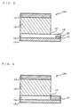
Fig. 2 shows the location of the second electrode 16
in the organic EL element 102 of the modification example
(No. 1) of the first embodiment, and an anode (second
electrode) 16 is formed on the surface of an extension 18
which is extended in the horizontal direction from the edge
section 17 of the semiconductor layer 14. Forming the
second electrode 16 at this kind of location can make the
electrically connected section between the second electrode
16 and the semiconductor layer 14 larger. Furthermore,
since the distance between the second electrode 16 and the
organic light-emitting medium 12 can be made longer,
occurrence of short-circuiting is able to be effectively
prevented. Furthermore, because the first electrode 10 and
the second electrode 16 are aligned in the same direction
and the top surface direction is exposed in Fig. 2,
electrical connection with the outside is made easy by
using this.
-
Fig. 3 shows the location of the second electrode 16
in the organic EL element 104 of the modified example (No.
2) of the first embodiment, in which there is the extension
18 extended in the horizontal direction from the edge
section 17 of the semiconductor layer 14, and the second
electrode 16 is formed on the side opposite to the side to
which the organic light-emitting medium 12 is located.
-
Forming the second electrode 16 at this kind of
location can make the electrically connected section
between the second electrode 16 and the semiconductor layer
14 larger, and occurrence of short-circuits is able to be
effectively prevented between the second electrode and the
organic light-emitting medium 12 without providing
electrical insulation treatment. In this example, by the
same reason as that shown in Fig. 1, an recessed section 22
is provided in the extension 18, in which the second
electrode 16 is formed.
-
Fig. 4 shows the location of the second electrode 16
in the organic EL element 106 of the modified example (No.
3) of the first embodiment. It shows that the second
electrode 16 is directly formed to the edge section (side
end) 17 of the semiconductor layer.
-
Forming the second electrode 16 at this kind of
location can make the configuration of the organic EL
element 106 in the lateral direction.
-
Fig. 5 shows a modification example (No. 4) of the
first embodiment, and shows an example in which the second
electrodes 16, 23 are provided in two places in the organic
EL elements 112. That is, it indicates that the second
electrodes 16, 23 are formed via the extension 18 to the
edge section (side end) 17 on both sides of the
semiconductor layer 14.
-
Forming a plurality of second electrodes 16, 23 in
this way can increase the contact area of these second
electrodes 16, 23 with the extension 18 in the
semiconductor layer 14, facilitating the injection of
electrons and holes. Even when continuity failure occurs
between either of the two electrodes 16, 23 and the
extension 18 in the semiconductor layer 14, continuity with
the other extended section 18 in the semiconductor layer 14
can be maintained with the other second electrode 16, 23.
-
Fig. 6 shows a modified example (No. 5) of the first
embodiment, in which a taper 24 is formed at the edge
section of the semiconductor layer 14, and on the taper,
the second electrode 16 is formed.
-
Forming the semiconductor layer 14 and the second
electrode 16 in the form of taper in this way can make the
contact area larger and facilitate injection of electrons
and holes.
-
In the modified example (No. 5) of the first
embodiment, the taper 24 is formed descending in the right
in Fig. 6, but conversely, this may be formed ascending in
the right. In the modified example (No. 5) of the first
embodiment, the cross-sectional profile in the taper 24 is
formed in a triangle in Fig. 6, but this cross-sectional
profile may be a trapezoid.
-
Fig. 7 shows a modified example (No. 6) of the first
embodiment, in which the semiconductor layer 9 is provided
on the first electrode 10 side. That is, it shows that the
first electrode 10 is formed at the edge section on the
side end of the semiconductor layer 9.
-
Forming the first electrode 10 in this way eliminates
the restriction to the kinds for the first electrode, while
since opaque low-resistance material may be used, injection
of electrons and holes becomes easier.
-
Fig. 8 shows the modified example (No. 7) of the
first embodiment, in which steps are formed at the edge
section of the semiconductor layer 14, and on the step, the
conductive layer 25 is formed, and on the conductive layer
25, the second electrode 16 is formed.
-
Bringing the semiconductor layer 14 to the second
electrode in the form of steps and further forming the
conductive layer 25 can increase the contact area and
facilitates the lowering of resistance.
-
Fig. 9 shows the connection condition and connection
position of the semiconductor layer 14 and the second
electrode 16. Fig. 9 (a) and (b) show plans, while Fig. 9
(c) and (d) show cross-sectional views.
-
This is preferable because taking this kind of form
can increase the contact area or because the excellent
connection reliability is obtained, the head end section of
the semiconductor layer 14 can be split as shown in Fig. 9
(a) or the head end section of the semiconductor layer 14
can be made into a hole structure as shown in Fig. 9 (b).
-
Because of the same reasons, it is preferable that as
shown in Fig. 9 (c), a recessed section is provided at the
head end section of the semiconductor layer 14 or a
triangle is formed at the head end section of the
semiconductor layer 14 as shown in Fig. 9 (d).
-
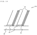
Fig. 10 shows the location of the second electrode 34
in the organic EL element 108 of the modified example (No.
8) of the first embodiment, indicating the condition with
the organic light-emitting medium, the first electrode, and
the like omitted. In this example, a plurality of second
electrodes 34 are patterned and installed in the form of
stripes. In addition, a plurality of semiconductor layers
32 are patterned and installed along the second electrode
34. And the second electrode 34 is electrically connected
along the edge section (side end) 36 of the semiconductor
layer 32.
-
Consequently, forming the second electrode 34 in this
kind of location can effectively prevent voltage drop by
the resistance at the semiconductor layer 32 (not
illustrated) by applying voltage across the first electrode
(not illustrated) and the second electrode 34.
-
When the second electrode 34 is formed at this kind
of location, for example, when the first electrode is
arranged vertically to the second electrode 34, the organic
EL element (pixels) 108 can be arranged in the matrix form.
Consequently, a large volume of the light energy can be
taken out from the light-emitting surface of the large-area
semiconductor layer 32, and at the same time, a thin-type
display device can be presented.
-
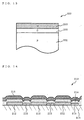
Fig. 11 shows the position of the second electrode 40
in the organic EL element 110 of the modified example (No.
9) of the first embodiment. Fig. 11 (a) indicates planely
that the second electrode 40 is patterned in the form of
lattices on the support substrate 42, and Fig. 11 (b)
indicates cross-sectionally that the semiconductor layer 44
is installed as if it covers the second electrode 40 and
partly exposed support substrate 42. Furthermore, Fig. 11
(c) shows cross-sectionally that in the organic EL element
110 in which the organic light-emitting medium 46 is formed
on the all over the semiconductor layer 44 shown in Fig. 11
(b), above which the patterned first electrode 48 is
formed, the light is taken out from the section shown with
symbol "T" to the outside.
-
Consequently, forming the second electrode 40 in this
kind of location can make the electrically connected
section between the second electrode 40 and the
semiconductor layer 22 be a large area, and the voltage
drop caused by the resistance at the semiconductor layer
can be effectively prevented. In addition, forming the
second electrode 40 in this kind of location, the organic
EL element (pixels) 110 can be arranged in a matrix by the
positional relationship with the first electrode (not
illustrated). And a large volume of light may be taken out
from the light-emitting surface of the large-area
semiconductor layer 44.
-
By the way, the second electrode may be included in
one pixel and the above-mentioned configuration may be
included in the semiconductor layer. Furthermore, the
configuration shown in Fig. 11 may be two-dimensionally
arranged as dots (part of the pixel) and may be formed in a
matrix.
(4) Support substrate
-
Next discussion will be made on the support substrate
15 in the organic EL element. If the support substrate
provides excellent mechanical strength and less
permeability of moisture and oxygen, the support substrate
which is generally used for this kind of an organic EL
element can be used as it is. Specifically, for example,
glass substrates, ceramic substrates, and the like 100 to
2,000 µm thick can be mentioned.
-
When the light is taken out to the outside via the
semiconductor layer formed on the support substrate, the
light transmittance of the relevant support substrate is
preferably 90% or more, and suitably 93% or more, and more
preferably 98% or more.
(5) Configuration examples
-
The organic EL element of the first embodiment has
the anode designated as the second electrode and the
cathode as the first electrode, and virtually has the
configuration of (i), but taking the configurations of the
organic EL element of (ii) through (iv) is preferable by
combining other component elements, such as hole injection
layer or electron injection layer.
-
It is also preferable to take the configurations (v)
through (viii) of the organic EL element with the anode
designated to the first electrode and the cathode to the
second electrode.
-
The preferable configuration examples (i) to (Viii)
of the organic EL element is specifically indicated as
follows:
- (i) Substrate/semiconductor layer (+ anode (second
electrode))/organic light-emitting layer/cathode (first
electrode)
- (ii) Substrate/semiconductor layer (+ anode)/hole injection
layer/organic light-emitting layer/cathode
- (iii) Substrate/semiconductor layer (+ anode)/organic
light-emitting layer/electron injection layer/cathode
- (iv) Substrate/semiconductor layer (+ anode)/hole injection
layer/organic light-emitting layer/electron injection layer
/cathode
- (v) Substrate/semiconductor layer (+ cathode (second
electrode))/organic light-emitting layer/anode (first
electrode)
- (vi) Substrate/semiconductor layer (+ cathode)/electron
injection layer/organic light-emitting layer/anode
- (vii) Substrate/semiconductor layer (+ cathode)/organic
light-emitting layer/hole injection layer/anode
- (viii) Substrate/semiconductor layer (+ cathode)/electron
injection layer/organic light-emitting layer/hole injection
layer/anode
-
-
Note that semiconductor layer (+ anode (second
electrode)), for example, means that an anode which is not
opposite to a cathode is provided with a semiconductor
layer.
[Second Embodiment]
-
Referring now to Fig. 12(a) to Fig. 12(d), the
manufacturing method of an organic EL element which is the
second embodiment according to the present invention will
be described in detail.
-
Fig. 12(a)-(d) is illustrations that schematically
show the organic EL element in each process(step) of the
manufacturing method related to the second embodiment. In
the following discussion, the manufacturing method of the
organic EL element is focused, and with respect to the
component materials, and the like, the contents described
for the first embodiment may apply.
(i) Formation of anode (second electrode)
-
Fig. 12(a) shows the condition in which the anode
(second electrode) 16 is installed on the support substrate
15.
-
The method for forming this anode 16 is not
particularly limited, but the anode may be able to be
formed in the specified location by combining sputtering
(deposition method) and photolithography. Specifically, on
the support substrate 15, the anode layer is formed on the
whole surface by the use of sputtering, and then, by using
photolithography, patterns are formed and the anode 16 is
accurately formed at the position which is electrically
connected to the edge section 17 of the semiconductor layer
14 in the future.
-
It is also possible to provide a recessed section at
the anode forming position on the support substrate, and to
align the top position of the support substrate to the
anode surface position to achieve flatness by forming the
anode at the recessed section. Consequently, forming the
anode in this manner enables accurate electrical connection
with the edge section of the semiconductor layer when the
semiconductor layer is formed in the subsequent (step). In
addition, forming the anode in this manner embeds the anode
in the electrically insulated support substrate and can
definitely maintain the electrical insulation with the
organic light-emitting medium to be formed in the
subsequent process(step) without using any electrically
insulating material.
(ii) Formation of semiconductor layer
-
Fig. 12(b) shows the condition in which the
semiconductor layer 14 is installed adjacent to the anode
(second electrode) 16 on the support substrate 15. That is,
the figure shows the condition in which the semiconductor
layer 14 is installed ready for electrical connection at
the end section 17.
-
The method for forming this semiconductor layer 14 is
not particularly limited, but for example, the
semiconductor layer 14 is able to be formed at the
specified location by sputtering (deposition) following the
preceding process(steps). That is, after etching the anode
layer in the preceding procedure, the resist is separated
and the semiconductor layer 14 is formed on the whole
surface and patterns are provided by photolithography
method, thereby forming the semiconductor layer 14 at the
specified location easily and in a short time.
-
When the semiconductor layer 14 is formed partly
overlapping with the anode 16, for example, the
semiconductor layer 14 is formed with the recessed section
22 provided as shown in Fig. 3, it is also preferable to
form the semiconductor layer 14 at the specified location
by further using photolithography.
(iii) Formation of organic light-emitting medium
-
Fig. 12(c) shows the condition in which the organic
light-emitting medium 12 is installed on the semiconductor
layer 14. The method of forming this organic light-emitting
medium is not particularly limited, but for example, the
organic light-emitting medium may be formed at the
specified location by the use of a shadow mask at the time
of deposition. In addition, when the organic light-emitting
medium 12 is composed with the light-emitting layer, hole
transport layer, hole injection layer, intermediate
interface layer, and the like, each layer is able to be
accurately formed by repeating the deposition process each
time.
-
In addition, when the organic light-emitting medium
12 is formed, it is preferably to coat the anode by
providing the electrical insulation layer (not
illustrated). By forming the electrical insulation layer in
this manner, the electrical insulation between the anode
and the organic light-emitting medium can be accurately
secured. Consequently, occurrence of short-circuits and the
cross-talking can be effectively prevented.
-
This kind of electrical insulation layer is
preferably composed with, for example, photo-curing type
epoxy resin, acrylic resin, siloxane resin, and the like.
For the layer that can replace the electrical insulation
layer, for example, non-charge injection type semiconductor
layer and metallic layer are mentioned.
(iv) Formation of cathode (first electrode)
-
Fig. 12(d) shows the condition in which the cathode
(first electrode) 10 is installed on the organic light-emitting
medium 12 and the organic EL element 106 is
configured. This cathode (first electrode) 10 can also be
formed at the specified location by combining, for example,
sputtering (deposition) and photolithography as described
above.
-
As described above, in the second embodiment, the
semiconductor layer 14 is formed after forming the anode
16, but it is also preferable to form the semiconductor
layer and the anode in the procedure reversal to this. That
is, by forming the semiconductor layer 14 first, and then
forming the anode 16, for example, the organic EL elements
100, 102, 108 can be easily fabricated as shown in Fig. 1,
Fig. 2, and Fig. 10. In addition to the case in which the
second electrode is formed on the substrate, the first
electrode is formed on the substrate and then the organic
light-emitting medium semiconductor layer is formed; then,
the second electrode may be formed at the edge section of
the semiconductor layer.
Examples
-
Referring now to the examples, the present invention
will be described further in detail as follows.
[Example 1]
(1) Fabrication of organic EL element
(i) Formation of the cathode (second electrode)
-
A transparent glass substrate having a dimension of
1.1 mm(thickness) × 200 mm (length) × 200 mm (width) was
ultrasonically cleaned and after drying in the N2 (nitrogen
gas) environment, the glass substrate was cleaned by the
use of UV (ultraviolet ray) and ozone further for 10
minutes. Then, on the cleaned glass substrate, a thin film
(100 nm thick) comprising Al/Si alloy (Si concentration: 1
at.%) was formed by the use of the sputtering apparatus
(available from ULVAC JAPAN, Ltd.). This Al/Si alloy thin
film was patterned in lattices (line width: 20 µm; lattice
pitch: 320 µm) by the use of photolithography as shown in
Fig. 11(a). The construction of the configuration in which
the cathode (second electrode) was electrically connected
at the edge section of the semiconductor layer was
intended.
(ii) Formation of the semiconductor layer
-
The glass substrate on which the cathode was formed
was cleaned with argon plasma, and then, on this glass
substrate, using the vacuum deposition apparatus (available
from ULVAC JAPAN, Ltd.), ZnSe and ZnCl2 with 150 nm film
thickness are simultaneously deposited to form the n-type
semiconductor layer. In addition, ZnSe deposition was
carried out at the vacuum of 1 x 10⁻⁶ Torr (1.33 x 10⁻⁴ Pa)
and at the temperature of 760 to 780°C, and ZnCl2 deposition
was carried out so that the specific resistance of the
semiconductor layer satisfied 3 x 10³ Ω · cm.
-
The charge concentration of the semiconductor layer
was measured by the four-terminal method and it was
confirmed that the charge concentration is 5 x 1015 cm-3.
(iii) Formation of the organic light-emitting medium
-
Then, the following component materials were
deposited successively to achieve each film thickness, and
the organic light-emitting medium was formed. By the way,
Alq functions as a light-emitting layer, NPD as a hole
transport layer, TPD74 as a hole injection layer, and CuPc
as an intermediate interface layer, respectively.
- Alq (A1 complex of 8-hydroxy-quinoline): 60 nm
- NPD (N,N'-di-(1-naphthyl)-N,N'-diphenyl-4, 4'-benzidine):
20 nm
- TPD74 (4,4'-bis-(N,N-di(m-tril)amino)-4"-phenyltriphenylamine):
20 nm
- CuPu (copper phthalocyanine): 20 nm
-
(iv) Formation of the anode (first electrode)
-
Lastly, for the anode (first electrode), Au was
deposited in 20 nm film thickness and Al in 100 nm film
thickness, and the organic EL element of Example 1 was
obtained.
(2) Assessment of the organic EL element
-
When in the organic EL element obtained, DC7V voltage
was applied across the anode (first electrode) and the
cathode (second electrode), green light emission was
obtained via the semiconductor layer. Then, the current
flew at 3 mA/cm2 and the emission luminance at that time was
54 cd/m2. Further, when the organic EL element was driven
at constant current with the initial emission luminance set
to 100 cd/m2, the 480-hour half-life was obtained.
[Example 2]
(1) Formation of organic EL element
(i) Formation of the anode (second electrode)
-
Same as Example 1, the Al/Si alloy thin film
patterned in the form of lattices (line width: 20 µm;
lattice pitch: 320 µm) was formed and designated it as the
anode (second electrode).
(ii) Formation of the semiconductor layer
-
The glass substrate with the anode formed was cleaned
with argon plasma, and then, on this glass substrate, using
the vacuum deposition apparatus (available from ULVAC
JAPAN, Ltd.), CdS and Cu are simultaneously deposited in 30
nm film thickness to form the p-type semiconductor layer.
The deposition was carried out at the vacuum of 1 x 10⁻⁶
Torr (1.33 x 10⁻⁴ Pa). and at the substrate temperature of
160°C, and Cu deposition was carried out so that the
specific resistance of the semiconductor layer satisfied 2
x 10 Ω · cm. The charge concentration of the semiconductor
layer was measured by the four-terminal method and it was
confirmed that the charge concentration is 4 x 1017 cm-3.
-
As described in "Applied Physics, 31, 1770 (1992),"
the semiconductor layer obtained that comprised a
combination of CdS and Cu was separately confirmed to
provide the properties as the p-type semiconductor.
(iii) Formation of the organic light-emitting medium
-
Then, TPD74, NPD, and Alq used in Example 1 were
deposited successively to form the organic light-emitting
medium with each film thickness of 200 nm, 20 nm, and 60
nm, respectively. By the way, TPD74 functions as a hole
injection layer, NPD as a hole transport layer, and Alq as
a light-emitting layer, respectively.
(iv) Formation of the cathode (first electrode)
-
Lastly, for the cathode (first electrode), LiF (0.5
nm) was deposited and, then, A1 was deposited in 200 nm
film thickness, and the organic EL element of Example 2 was
obtained.
(2) Assessment of the organic EL element
-
When in the organic EL element obtained, DC7V voltage
was applied across the cathode (first electrode) and the
anode (second electrode), green light emission was obtained
via the semiconductor layer. Then, the 2.7 mA/cm2 current
flew and the emission luminance at that time was 32 cd/m2.
Further, when the organic EL element was driven at constant
current with the initial emission luminance set to 100
cd/m2, the 620-hour half-life was obtained.
[Example 3]
(1) Fabrication of organic EL element
-
In Example 3, effects of the organic semiconductor
layer were investigated. That is, in place of the
semiconductor layer comprising a combination of CdS and Cu
in Example 2, a 70-nm-film thickness semiconductor layer
comprising PEDOT (3,4-polyethylene dioxythiophene,
available from Bayer), which is polymer indicating
semiconductance, was spin-coated in the condition of the
aqueous solution, and then, was vacuum-dried to form an
organic EL element, with others all same as Example 2.
(2) Assessment of the organic EL element
-
When DC7V voltage was applied across the cathode
(first electrode) and the anode (second electrode), the 5.2
mA/cm2 current flew and green light emission which emission
luminance was 180 cd/m2 was obtained via the semiconductor
layer. Then, when the organic EL element was driven at
constant current with the initial emission luminance set to
100 cd/m2, the 790-hour half-life was obtained. The results
obtained are shown in Table 1.
-
When the surface resistance of the semiconductor
layer was measured, 1.6 kΩ was obtained and the specific
resistance was 1.1 x 10² Ω · cm.
[Comparative example 1]
(1) Fabrication of organic EL element
-
The organic EL element was fabricated in the same
manner as Example 1, with an exception of not forming the
patterned (line width: 20 µm; lattice pitch: 320 µm) Al/Si
alloy thin film (cathode).
(2) Assessment of the organic EL element
-
When DC7V voltage was applied across the
semiconductor layer and the anode (first electrode) in the
organic EL element obtained, only a spot-like light
emission about 5 mm in diameter was obtained near the place
where the electricity was fed to the semiconductor layer.
-
That is, even when the voltage was directly applied
to the semiconductor layer with resistance as high as 3 x
103 Ω·cm without the second electrode, the light was
scarcely emitted and the organic element obtained did not
function as the organic EL element.
[Comparative example 2]
(1) Fabrication of organic EL element
-
The organic EL element was fabricated in the same
manner as Example 1, with an exception of not patterning in
lattices the Al/Si alloy thin film (cathode) in Example 1
but forming the film throughout the whole surface.
(2) Assessment of the organic EL element
-
When DC7V voltage was applied across the Al/Si alloy
thin film and Au/Al (cathode) in the organic EL element
obtained, 3.6 mA/cm2 current flew and the light emission was
0.6 cd/m2. That is, the light energy that can be taken out
the outside was lowered to about 1/50 as compared to
Example 1. It was assumed that when the light was taken out
to the outside via the cathode formed throughout the whole
surface and the semiconductor layer, EL light emission may
be absorbed by he cathode and the semiconductor layer.
-
Consequently, the superiority of patterning the Al/Si
alloy thin film (cathode) and electrically connecting to
the edge section of the semiconductor layer as in the case
of Example 1 was identified.
| | Example 1 | Example 2 | Example 3 | Comparative example 1 | Comparative example 2 |
| Second electrode | Patterned cathode | Patterned anode | Patterned anode | Non-None | patterned cathode |
| Semi-conductor layer | ZnSe/ZnCl2 | CdS/Cu | PEDOT | ZnSe/ZnCl2 | ZnSe/ZnCl2 |
| EL light emission take-out surface | Semi-conductor layer | Semi-conductor layer | Semi-conductor layer | Semi-conductor layer | Cathode/ Semi-conductor layer |
| Luminance (cd/m2) | 54 | 32 | 180 | Spot like emission | 0.6 |
| Half-life (hours) | 480 | 620 | 790 | 0 | 0 |
Industrial Applicability
-
According to the organic EL element of the present
invention, the first electrode and the second electrode
were no longer necessary to be brought virtually opposite
to each other by installing an organic light emitting
medium between the first electrode (anode or cathode) and
the semiconductor layer comprising the non-monocrystal
material and electrically connecting the second electrode
(cathode or anode) to the edge section of the semiconductor
layer. Consequently, the following effects have been able
to be obtained.
- (i) Because the first electrode and the second electrode
are not virtually opposite to each other, the EL light
emission is able to be taken out form the semiconductor
layer to the outside.
Consequently, electrode materials which have been
unable to be used due to the relation of light
transmittance, and the like can be used, and the selection
range has been remarkably increased. For example, low-resistance
metallic materials have been able to be used,
and consequently, low-voltage drive is enabled, and an
organic EL element whose consumption power is low and
response speed is high can be supplied.In addition, even when the EL light emission is taken
out from the semiconductor layer, since the second
electrode is installed at the edge section of the
semiconductor layer, the second electrode does not shield
the light and the EL light emission has been able to be
taken out efficiently to the outside.Furthermore, the blue light emission which used to be
absorbed at the semiconductor monocrystal and was difficult
to be taken out due to the relation of light transmittance
has been able to be efficiently taken out to he outside.
- (ii) Because the semiconductor layer is formed by the non-monocrystal
material, a large-area semiconductor layer has
been able to be formed efficiently. Consequently, by
forming the organic light-emitting medium and the like on
this kind of semiconductor layer, an organic EL element
with uniform properties and a large area has been able to
be presented.
- (iii) Because the second electrode is located in the
lateral direction of the organic light-emitting medium,
short-circuits of the second and the first electrodes has
been able to be prevented. That is, because short-circuits
result in display failure of the element, this kind of
display failure has been able to be completely eliminated
by the configuration of the present invention.
- (iv) When the inorganic semiconductor material is used for
the semiconductor layer, an organic EL element that
provides superb heat resistance and durability, and is free
of separation of the semiconductor layer and the second
electrode even if the element can be driven, for example,
for more than 1000 hours, and at the same time achieves
little degradation of luminance can be presented.
-
-
In addition, according to the manufacturing method of
the organic EL element of the present invention, when
either of the anode or the cathode is designated to the
first electrode and the other electrode to the second
electrode, the selectivity of order of each forming
process(step) has become increased by including a step for
the second electrode, a step for forming the semiconductor
layer at the position connectable to the second electrode
edge section by the use of non-monocrystal material, a step
for forming the organic light-emitting medium, and a step
for forming the first electrode. Because the non-monocrystal
material is used for the semiconductor layer,
an organic EL element which provides uniform properties and
a large area are able to be easily manufactured. In
addition, since there is no need to form the first
electrode and the second electrode opposite to each other,
the light energy take out is able to be increased, and at
the same time, a wide variety of electrode materials have
been able to be used.