EP1124314A1 - Ladungspumpenvorrichtung - Google Patents
Ladungspumpenvorrichtung Download PDFInfo
- Publication number
- EP1124314A1 EP1124314A1 EP01200428A EP01200428A EP1124314A1 EP 1124314 A1 EP1124314 A1 EP 1124314A1 EP 01200428 A EP01200428 A EP 01200428A EP 01200428 A EP01200428 A EP 01200428A EP 1124314 A1 EP1124314 A1 EP 1124314A1
- Authority
- EP
- European Patent Office
- Prior art keywords
- transistor
- potential
- charge pump
- stage
- node
- Prior art date
- Legal status (The legal status is an assumption and is not a legal conclusion. Google has not performed a legal analysis and makes no representation as to the accuracy of the status listed.)
- Granted
Links
- 230000005669 field effect Effects 0.000 claims abstract description 7
- 230000004913 activation Effects 0.000 claims description 11
- 239000003990 capacitor Substances 0.000 abstract description 5
- 239000007858 starting material Substances 0.000 abstract 3
- 238000001994 activation Methods 0.000 description 10
- 238000010586 diagram Methods 0.000 description 9
- 230000000694 effects Effects 0.000 description 3
- 101000817602 Rattus norvegicus Dynamin-1 Proteins 0.000 description 2
- 230000015556 catabolic process Effects 0.000 description 1
- 230000000295 complement effect Effects 0.000 description 1
- 238000006731 degradation reaction Methods 0.000 description 1
- 230000006866 deterioration Effects 0.000 description 1
- 238000005265 energy consumption Methods 0.000 description 1
Images


Classifications
-
- H—ELECTRICITY
- H02—GENERATION; CONVERSION OR DISTRIBUTION OF ELECTRIC POWER
- H02M—APPARATUS FOR CONVERSION BETWEEN AC AND AC, BETWEEN AC AND DC, OR BETWEEN DC AND DC, AND FOR USE WITH MAINS OR SIMILAR POWER SUPPLY SYSTEMS; CONVERSION OF DC OR AC INPUT POWER INTO SURGE OUTPUT POWER; CONTROL OR REGULATION THEREOF
- H02M3/00—Conversion of DC power input into DC power output
- H02M3/02—Conversion of DC power input into DC power output without intermediate conversion into AC
- H02M3/04—Conversion of DC power input into DC power output without intermediate conversion into AC by static converters
- H02M3/06—Conversion of DC power input into DC power output without intermediate conversion into AC by static converters using resistors or capacitors, e.g. potential divider
- H02M3/07—Conversion of DC power input into DC power output without intermediate conversion into AC by static converters using resistors or capacitors, e.g. potential divider using capacitors charged and discharged alternately by semiconductor devices with control electrode, e.g. charge pumps
- H02M3/073—Charge pumps of the Schenkel-type
Definitions
- the present invention relates to a charge pump device comprising scaling a plurality of stages to transfer a potential charge from one stage to the next in response to clock signals.
- Each floor includes, arranged between an input and an output thereof, a switching circuit and a capacitance storage.
- the switching circuit is formed by a first transistor mounted with a second transistor, the drains of the first and second transistors being connected to the input of the stage, the source of the first transistor being connected to the gate of the second transistor and the source of the second transistor being connected to the output of the stage and to the gate of the first transistor.
- the gate of the second transistor is controlled by one of the clock signals for example via a capacitor.
- a Dickson type charge pump is commonly used in devices such as EEPROMs, for example, which require strong voltage rise from a relatively low available voltage.
- a pump Dickson type of charge essentially consists of a plurality of stages arranged in a ladder. Each stage of the pump includes an active device which conducts current in one direction and a storage capacity.
- Figure 1 shows an example of another embodiment of a charge pump. Floors 1 to N are connected in scale to each other by an active switching device 10, 20 formed of two transistors 11, 12.
- the choice to use a circuit of two transistors rather than a simple transistor connected in diode (the drain is connected with the grid) avoids falls of charge pump voltage due to the effects of threshold voltages inherent in transistors connected by diode. Indeed, for a diode-connected transistor, the threshold voltage can be 2V or more, thus limiting a minimum Vin voltage usable at 2V or more.
- the switching circuit 10, 20 is controlled by clock signals PA, PB via a Co capacitor which reduces the voltage drop in the switching circuit.
- the charge pump then presents an almost ideal multiplication factor, which provides a higher output voltage Vout.
- This charge pump is conventionally controlled by a quadriphase clock with PHI, PA, PHINOT signals, PB not interleaved as illustrated in figure 2.
- the charge pump is switched on operation by application of the four clock signals PHI, PA, PHINOT, PB to the plurality of stages 1 to N.
- the pump is put out of operation by stopping the application of clock signals or by a device which interrupts the delivery of the raised output signal Vout.
- the operating mode of the charge pump is explained with reference in FIGS. 3 and 4. It is assumed that all the internal nodes of the device for switching 10, 20 are at zero potential before starting the pump.
- FIG. 3 shows the configuration of the stage during an active CPA sequence of the clock PHI signal.
- the transistor 11 is in a blocked state (OFF) which prevents the current from flowing and the transistor 12 is in a passing state (ON) authorizing the passage of the current.
- the potential VA i at node A i is equivalent to the potential VA i + 1 at node A i + 1 .
- This first sequence corresponds to a phase of elevation of the potentials VA i and VA i + 1 according to the capacitive load of the capacitor Cb which flows through the transistor 12 in the capacitor Ca.
- Figure 4 shows the configuration of a pump stage during an inactive sequence CPA of the clock PHI signal.
- Transistor 11 is in the on state, while transistor 12 is in the off state preventing current from flowing from node A i to node A i + 1 .
- the potential VA i at node A i is equivalent to the potential Vc at node c junction point of the source of transistor 11 with the gate of transistor 12.
- Such regular operation of the charge pump can only be implemented on condition that initially the internal nodes of the switching device 10 are at zero potential.
- certain internal nodes in the plurality of capacitive stages N retain voltage potentials having values between 0 volts and Vout after a sequence of charging the pump. This causes problems during the next start of the pump which lead to a deterioration in the elevation of the Vin signal in most cases and to no elevation of the Vin signal in the worst cases.
- the node c in one or more stages memorizes a voltage on the capacitance Co greater than the potential VA i + 1 of the node A i + 1 , which polarizes the transistor 12 in the on state .
- the node A i + 1 is at a potential VA i + 1 close to the potential VA i of the node A i . Since the potential VA i + 1 plays the role of control voltage for the transistor 11, the latter remains in the blocked state then preventing any discharge of the potential Vc from the node c in the circuit. Consequently, in this case, the next start-up of the pump cannot be carried out normally since one or more stages remain permanently blocked in the configuration shown in FIG. 3, which results in an alternative charge transfer between the capacities Ca and Cb, preventing the charge pump effect from occurring.
- Figure 5 illustrates two consecutive charge cycles D1 and D2.
- the first charge cycle D1 shows that the pump has started in ideal conditions, i.e. without any internal node loaded while the second consecutive cycle D2 shows the load degradation in the pump when it has memorized potentials in its internal nodes during the previous charge cycle D1.
- a PMOS transistor is in a passing state when the potential of its gate is less than the potential of its source by at least one threshold voltage (Vt) of the transistor.
- This threshold voltage depends in particular on the voltage applied to the source of the transistor.
- Vt can vary approximately between 0.7 V and 3 V, respectively, for a low voltage applied to the source of the transistor, of the order of a volt, and for a high voltage applied to the source of the transistor, of the order of ten volts.
- the present invention aims to remedy the aforementioned drawbacks of the art prior and, in particular, to realize a charge pump device which restores, between each activation of the pump, the potential conditions required for a optimal functioning of the switching circuit at start-up and this also with reduced energy consumption.
- a charge pump device as defined in the field of the invention above and characterized in that at least one of the stages further comprises starting means, at a node c of junction of the source of the first transistor with the gate of the second transistor having a potential Vc, to maintain the second transistor in a blocked state between two charge cycles of the charge pump device.
- the charge pump device comprises a plurality of stages, each being provided with starting means.
- the starting means comprise means for maintaining the potential Vc of the node c at a value less than or equal to that of a potential at the output of the floor.
- the junction node of the source of the first transistor with the gate of the second transistor is kept at a lower potential value than that of the source of this second transistor, which keeps the latter in a state blocked between two pump activations.
- the starting means comprise means for maintaining the potential Vc of the node c at a value greater than or equal to that of a potential at the output of the 'floor.
- the junction node of the source of the first transistor with the gate of the second transistor is maintained at a higher potential value than that of its source, which keeps the second transistor in a blocked state between two activations of the pump.
- the starting means comprise a switch arranged between the junction node and a grounding terminal.
- the knot of junction is then discharged of its potential.
- the starting means include a switch disposed between the junction node and the output of the floor. The minimum condition for maintaining the second transistor in a blocked state is then carried out.
- the means of start-up include a switch arranged between the junction node and a source of positive potential.
- the switch circuit and the starting means are then adapted to the charge pump according to the invention for operation in reverse current.
- the charge pump device can either include first and second transistors of the bipolar transistor type or junction, junction field effect (FET) or insulated gate field effect (MOS).
- FET junction field effect
- MOS insulated gate field effect
- the starting means comprise a resistor placed between the switch and the earth potential. A resistive link between the junction node and the earth potential is then established.
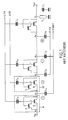
- FIG. 6 represents a charge pump according to the invention comprising elements of the charge pump described in relation to the prior art and means complementary start-up 300 according to a first embodiment.
- the pump load comprises in particular a plurality of stages 1 to N arranged in a scale, each comprising, in a known manner, a switching circuit 100, 200 and a capacitance Ca, Cb, the switching circuit being formed by the connection of a first transistor 110 and a second transistor 120.
- the pump is charged conventionally in response to PHI, PA, PHINOT, PB signals not interleaved with a quadriphase clock.
- these signals will, for the sake of energy saving, peak voltage less than 3 volts or substantially equal at this value.
- the starting means 300 comprise a switch 310 connected on one side to a node c connecting the source of the first transistor 110 with the gate of the second transistor 120 and on the other hand to a grounding terminal V ss .
- the charge pump has a means of securing the start before each activation phase thereof. Indeed, as the node c is discharged of its potential in the grounding terminal V ss by closing the switch 310, the second transistor 120 can then be placed in a blocked state for sure before any pump start-up because then the potential Vc at node c is less than or equal to a potential VA i + 1 at node A i + 1 which corresponds to the potential of the source of the second transistor 120.
- the switch 310 can then be controlled by a device which makes it possible to determine whether a raised voltage Vout is required at the output of the pump or not.
- the switch is preferably activated (ON) between each activation cycle of the charge pump device. It is deactivated (OFF) each time this device is activated to deliver a raised voltage.
- all the switches are activated simultaneously using a control signal supplied by an electronic circuit arranged to control these switches.
- a resistor R D can be placed between the switch 310 and the earth potential tap V ss to establish a resistive link between the potential Vc at node c and the earth terminal V ss .
- a resistance is provided high value without switch to form the starting means.
- Figure 7 shows two successive charge cycles of the D100 pump and D200 where the starting means 300 have been implemented as explained previously between the two activations. There is a perfect symmetry of D200 activation with D100 activation unlike D2 activation in Figure 5 obtained with a charge pump used without the starting means of the invention.
- a charge pump according to the invention can already be secured at start-up with a single stage or a subset of stages among stages 1 to N equipped the aforementioned starting means. Preferably, all of the floors include these starting means.
- FIG. 8 shows a stage of a charge pump equipped with starting means 400 in accordance with a second embodiment of the invention.
- the node c is connected to the node A i + 1 by a switch 410 which, when closed, short-circuits the node c with the node A i + 1 .
- the potential Vc at node c is then close to the potential VA i + 1 at node A i + 1 , which prevents the gate potential of transistor 120 from being greater than the source potential of the same transistor. Under these conditions, the transistor 120 cannot be in a conducting state and then realizes the necessary condition of state of the transistor 12 at the start of the pump, that is to say to be in a blocked state.
- this charging pump can comprise one, several or all of its stages equipped with the switch 410 depending on the conditions d 'desired use.
- the first and second embodiments have been described in relation to a switching circuit 100, 200 which operates in direct current (transistors 110 and 120 N channel type).
- FIG. 9 represents a stage of a charge pump equipped with starting means 500 in accordance with a third embodiment of the invention.
- This third embodiment corresponds to an operation in reverse current of the switching circuit 100, 200 in the charge pump with respect to the corresponding operation of the first and second embodiments.
- the switching circuit 100, 200 of each stage comprises a first and a second transistor 130, 140 with an inverted channel (P channel) with respect to the transistors 110, 120. Consequently, the conditions required for starting pump safety are also reversed.
- the potential Vc of the gate of transistor 140 must be greater than or equal to the potential VA i + 1 of node A i + 1 to place the transistor in the off state.
- the starting means 500 are formed of a switch 510 arranged between the node c and a positive potential V DD in this third embodiment.
- the node c is set to a potential which is greater than the potential VA i + 1 carrying out the blocked state of the transistor 140 before any start-up of the charge pump.
- This third embodiment has the same performances as those described for the first and second embodiments according to the invention.
- the switching circuit 100, 200 can be implemented as well with insulated gate field effect (MOS) transistors than transistors bipolar or junction field effect transistors (FET).
- MOS insulated gate field effect
- FET junction field effect transistors
Landscapes
- Engineering & Computer Science (AREA)
- Power Engineering (AREA)
- Dc-Dc Converters (AREA)
Priority Applications (1)
| Application Number | Priority Date | Filing Date | Title |
|---|---|---|---|
| EP20010200428 EP1124314B1 (de) | 2000-02-09 | 2001-02-06 | Ladungspumpenvorrichtung |
Applications Claiming Priority (3)
| Application Number | Priority Date | Filing Date | Title |
|---|---|---|---|
| EP00102692 | 2000-02-09 | ||
| EP00102692 | 2000-02-09 | ||
| EP20010200428 EP1124314B1 (de) | 2000-02-09 | 2001-02-06 | Ladungspumpenvorrichtung |
Publications (2)
| Publication Number | Publication Date |
|---|---|
| EP1124314A1 true EP1124314A1 (de) | 2001-08-16 |
| EP1124314B1 EP1124314B1 (de) | 2009-01-07 |
Family
ID=26070522
Family Applications (1)
| Application Number | Title | Priority Date | Filing Date |
|---|---|---|---|
| EP20010200428 Expired - Lifetime EP1124314B1 (de) | 2000-02-09 | 2001-02-06 | Ladungspumpenvorrichtung |
Country Status (1)
| Country | Link |
|---|---|
| EP (1) | EP1124314B1 (de) |
Cited By (1)
| Publication number | Priority date | Publication date | Assignee | Title |
|---|---|---|---|---|
| EP1278202A3 (de) * | 2001-06-26 | 2004-06-16 | Sharp Kabushiki Kaisha | Nichtflüchtige Halbleiterspeicheranordnung |
Citations (4)
| Publication number | Priority date | Publication date | Assignee | Title |
|---|---|---|---|---|
| US4734599A (en) * | 1985-04-30 | 1988-03-29 | Hughes Aircraft Company | Circuit for multiplying a pump clock voltage |
| US5798915A (en) * | 1997-01-29 | 1998-08-25 | Microchip Technology Incorporated | Progressive start-up charge pump and method therefor |
| WO1999003192A1 (en) * | 1997-07-10 | 1999-01-21 | Microchip Technology Incorporated | A progressive start-up charge pump and method therefor |
| US5973979A (en) * | 1996-02-15 | 1999-10-26 | Advanced Micro Devices, Inc. | Low supply voltage negative charge pump |
-
2001
- 2001-02-06 EP EP20010200428 patent/EP1124314B1/de not_active Expired - Lifetime
Patent Citations (4)
| Publication number | Priority date | Publication date | Assignee | Title |
|---|---|---|---|---|
| US4734599A (en) * | 1985-04-30 | 1988-03-29 | Hughes Aircraft Company | Circuit for multiplying a pump clock voltage |
| US5973979A (en) * | 1996-02-15 | 1999-10-26 | Advanced Micro Devices, Inc. | Low supply voltage negative charge pump |
| US5798915A (en) * | 1997-01-29 | 1998-08-25 | Microchip Technology Incorporated | Progressive start-up charge pump and method therefor |
| WO1999003192A1 (en) * | 1997-07-10 | 1999-01-21 | Microchip Technology Incorporated | A progressive start-up charge pump and method therefor |
Cited By (1)
| Publication number | Priority date | Publication date | Assignee | Title |
|---|---|---|---|---|
| EP1278202A3 (de) * | 2001-06-26 | 2004-06-16 | Sharp Kabushiki Kaisha | Nichtflüchtige Halbleiterspeicheranordnung |
Also Published As
| Publication number | Publication date |
|---|---|
| EP1124314B1 (de) | 2009-01-07 |
Similar Documents
| Publication | Publication Date | Title |
|---|---|---|
| EP1079525B1 (de) | System zur Steuerung eines Zweirichtungs-Schalters mit zwei Transistoren | |
| EP0579561B1 (de) | Schutzschaltung gegen Überspannungen für Leistungsbauteil | |
| EP1950885B1 (de) | Steuervorrichtung eines elektronischen Leistungstrenners und eine solche Vorrichtung umfassender Stromrichter | |
| FR2689294A1 (fr) | Circuit de pompage de tension à utiliser dans des dispositifs de mémoire à semi-conducteur. | |
| EP0215707A1 (de) | Spannungsschaltvorrichtung | |
| FR2863118A1 (fr) | Circuit onduleur | |
| FR2848356A1 (fr) | Procede de commande d'une alimentation a decoupage a un seul element inductif et plusieurs sorties, et alimentation correspondante, en particulier pour un telephone mobile cellulaire | |
| EP1704634A1 (de) | Steuerung eines kurzschlusses in einer induktivität eines aufwaertswandlers | |
| EP1864381A2 (de) | Mos-steuerung für transistoren | |
| EP3032729B1 (de) | Gleichstrom-gleichstrom-wandler mit kaltstart | |
| EP3883105A1 (de) | Vorrichtung zum entladen eines kondesators | |
| FR2732833A1 (fr) | Unite integree de commande de puissance a faible dissipation | |
| WO2014091096A1 (fr) | Circuit de comparaison d'une tension a un seuil et conversion d'energie electrique | |
| EP4068606B1 (de) | Spannungswandler | |
| EP1986314A1 (de) | Steuerverfahren eines Schaltnetzteils mit einem einzigen induktiven Element und mehreren Ausgängen, sowie entsprechende Schaltnetzteilvorrichtung, insbesondere für ein Mobiltelefon | |
| EP1124314B1 (de) | Ladungspumpenvorrichtung | |
| EP0928060A1 (de) | Gleichspannungswandler mit verbessertem Wirkungsgrad | |
| WO2020011768A1 (fr) | Procede de declenchement de la mise a l'etat passant d'un transistor | |
| FR2802698A1 (fr) | Circuit de lecture de charges protege contre des surcharges provenant de charges de polarite non desiree | |
| EP0119927B1 (de) | Hochspannungsverstärker für kapazitive Last | |
| EP3651363A1 (de) | Adiabatische logische zelle | |
| FR3094853A1 (fr) | Circuit de commande de transistors | |
| FR2884072A1 (fr) | Procede de controle du fonctionnement d'une pompe de charge et circuit integre de pompe de charge correspondant | |
| FR3146561A1 (fr) | Circuit de modulation de largeur d'impulsion | |
| FR3146522A1 (fr) | Circuit de détection d'un court-circuit |
Legal Events
| Date | Code | Title | Description |
|---|---|---|---|
| PUAI | Public reference made under article 153(3) epc to a published international application that has entered the european phase |
Free format text: ORIGINAL CODE: 0009012 |
|
| AK | Designated contracting states |
Kind code of ref document: A1 Designated state(s): AT BE CH CY DE DK ES FI FR GB GR IE IT LI LU MC NL PT SE TR |
|
| AX | Request for extension of the european patent |
Free format text: AL;LT;LV;MK;RO;SI |
|
| 17P | Request for examination filed |
Effective date: 20020218 |
|
| AKX | Designation fees paid |
Free format text: AT BE CH CY DE DK ES FI FR GB GR IE IT LI LU MC NL PT SE TR |
|
| GRAP | Despatch of communication of intention to grant a patent |
Free format text: ORIGINAL CODE: EPIDOSNIGR1 |
|
| GRAS | Grant fee paid |
Free format text: ORIGINAL CODE: EPIDOSNIGR3 |
|
| GRAA | (expected) grant |
Free format text: ORIGINAL CODE: 0009210 |
|
| AK | Designated contracting states |
Kind code of ref document: B1 Designated state(s): AT BE CH CY DE DK ES FI FR GB GR IE IT LI LU MC NL PT SE TR |
|
| REG | Reference to a national code |
Ref country code: GB Ref legal event code: FG4D Free format text: NOT ENGLISH |
|
| REG | Reference to a national code |
Ref country code: CH Ref legal event code: EP |
|
| REG | Reference to a national code |
Ref country code: IE Ref legal event code: FG4D Free format text: LANGUAGE OF EP DOCUMENT: FRENCH |
|
| REF | Corresponds to: |
Ref document number: 60137278 Country of ref document: DE Date of ref document: 20090226 Kind code of ref document: P |
|
| REG | Reference to a national code |
Ref country code: CH Ref legal event code: NV Representative=s name: ICB INGENIEURS CONSEILS EN BREVETS SA |
|
| PG25 | Lapsed in a contracting state [announced via postgrant information from national office to epo] |
Ref country code: NL Free format text: LAPSE BECAUSE OF FAILURE TO SUBMIT A TRANSLATION OF THE DESCRIPTION OR TO PAY THE FEE WITHIN THE PRESCRIBED TIME-LIMIT Effective date: 20090107 |
|
| NLV1 | Nl: lapsed or annulled due to failure to fulfill the requirements of art. 29p and 29m of the patents act | ||
| PG25 | Lapsed in a contracting state [announced via postgrant information from national office to epo] |
Ref country code: ES Free format text: LAPSE BECAUSE OF FAILURE TO SUBMIT A TRANSLATION OF THE DESCRIPTION OR TO PAY THE FEE WITHIN THE PRESCRIBED TIME-LIMIT Effective date: 20090418 Ref country code: FI Free format text: LAPSE BECAUSE OF FAILURE TO SUBMIT A TRANSLATION OF THE DESCRIPTION OR TO PAY THE FEE WITHIN THE PRESCRIBED TIME-LIMIT Effective date: 20090107 |
|
| REG | Reference to a national code |
Ref country code: IE Ref legal event code: FD4D |
|
| BERE | Be: lapsed |
Owner name: EM MICROELECTRONIC-MARIN SA Effective date: 20090228 |
|
| PG25 | Lapsed in a contracting state [announced via postgrant information from national office to epo] |
Ref country code: PT Free format text: LAPSE BECAUSE OF FAILURE TO SUBMIT A TRANSLATION OF THE DESCRIPTION OR TO PAY THE FEE WITHIN THE PRESCRIBED TIME-LIMIT Effective date: 20090608 Ref country code: AT Free format text: LAPSE BECAUSE OF FAILURE TO SUBMIT A TRANSLATION OF THE DESCRIPTION OR TO PAY THE FEE WITHIN THE PRESCRIBED TIME-LIMIT Effective date: 20090107 Ref country code: SE Free format text: LAPSE BECAUSE OF FAILURE TO SUBMIT A TRANSLATION OF THE DESCRIPTION OR TO PAY THE FEE WITHIN THE PRESCRIBED TIME-LIMIT Effective date: 20090407 |
|
| PG25 | Lapsed in a contracting state [announced via postgrant information from national office to epo] |
Ref country code: MC Free format text: LAPSE BECAUSE OF NON-PAYMENT OF DUE FEES Effective date: 20090228 |
|
| PG25 | Lapsed in a contracting state [announced via postgrant information from national office to epo] |
Ref country code: DK Free format text: LAPSE BECAUSE OF FAILURE TO SUBMIT A TRANSLATION OF THE DESCRIPTION OR TO PAY THE FEE WITHIN THE PRESCRIBED TIME-LIMIT Effective date: 20090107 Ref country code: IE Free format text: LAPSE BECAUSE OF FAILURE TO SUBMIT A TRANSLATION OF THE DESCRIPTION OR TO PAY THE FEE WITHIN THE PRESCRIBED TIME-LIMIT Effective date: 20090107 |
|
| PLBE | No opposition filed within time limit |
Free format text: ORIGINAL CODE: 0009261 |
|
| STAA | Information on the status of an ep patent application or granted ep patent |
Free format text: STATUS: NO OPPOSITION FILED WITHIN TIME LIMIT |
|
| REG | Reference to a national code |
Ref country code: FR Ref legal event code: ST Effective date: 20091030 |
|
| 26N | No opposition filed |
Effective date: 20091008 |
|
| GBPC | Gb: european patent ceased through non-payment of renewal fee |
Effective date: 20090407 |
|
| PG25 | Lapsed in a contracting state [announced via postgrant information from national office to epo] |
Ref country code: DE Free format text: LAPSE BECAUSE OF NON-PAYMENT OF DUE FEES Effective date: 20090901 |
|
| REG | Reference to a national code |
Ref country code: FR Ref legal event code: RN |
|
| PG25 | Lapsed in a contracting state [announced via postgrant information from national office to epo] |
Ref country code: BE Free format text: LAPSE BECAUSE OF NON-PAYMENT OF DUE FEES Effective date: 20090228 |
|
| PG25 | Lapsed in a contracting state [announced via postgrant information from national office to epo] |
Ref country code: FR Free format text: LAPSE BECAUSE OF NON-PAYMENT OF DUE FEES Effective date: 20090309 Ref country code: GB Free format text: LAPSE BECAUSE OF NON-PAYMENT OF DUE FEES Effective date: 20090407 |
|
| REG | Reference to a national code |
Ref country code: FR Ref legal event code: FC |
|
| PGRI | Patent reinstated in contracting state [announced from national office to epo] |
Ref country code: DE Effective date: 20100215 |
|
| PGRI | Patent reinstated in contracting state [announced from national office to epo] |
Ref country code: FR Effective date: 20100511 |
|
| PG25 | Lapsed in a contracting state [announced via postgrant information from national office to epo] |
Ref country code: GR Free format text: LAPSE BECAUSE OF FAILURE TO SUBMIT A TRANSLATION OF THE DESCRIPTION OR TO PAY THE FEE WITHIN THE PRESCRIBED TIME-LIMIT Effective date: 20090408 |
|
| PG25 | Lapsed in a contracting state [announced via postgrant information from national office to epo] |
Ref country code: IT Free format text: LAPSE BECAUSE OF FAILURE TO SUBMIT A TRANSLATION OF THE DESCRIPTION OR TO PAY THE FEE WITHIN THE PRESCRIBED TIME-LIMIT Effective date: 20090107 |
|
| PG25 | Lapsed in a contracting state [announced via postgrant information from national office to epo] |
Ref country code: LU Free format text: LAPSE BECAUSE OF NON-PAYMENT OF DUE FEES Effective date: 20090206 |
|
| PG25 | Lapsed in a contracting state [announced via postgrant information from national office to epo] |
Ref country code: TR Free format text: LAPSE BECAUSE OF FAILURE TO SUBMIT A TRANSLATION OF THE DESCRIPTION OR TO PAY THE FEE WITHIN THE PRESCRIBED TIME-LIMIT Effective date: 20090107 |
|
| PG25 | Lapsed in a contracting state [announced via postgrant information from national office to epo] |
Ref country code: CY Free format text: LAPSE BECAUSE OF FAILURE TO SUBMIT A TRANSLATION OF THE DESCRIPTION OR TO PAY THE FEE WITHIN THE PRESCRIBED TIME-LIMIT Effective date: 20090107 |
|
| REG | Reference to a national code |
Ref country code: FR Ref legal event code: PLFP Year of fee payment: 16 |
|
| REG | Reference to a national code |
Ref country code: FR Ref legal event code: PLFP Year of fee payment: 17 |
|
| REG | Reference to a national code |
Ref country code: FR Ref legal event code: PLFP Year of fee payment: 18 |
|
| PGFP | Annual fee paid to national office [announced via postgrant information from national office to epo] |
Ref country code: DE Payment date: 20200121 Year of fee payment: 20 |
|
| PGFP | Annual fee paid to national office [announced via postgrant information from national office to epo] |
Ref country code: CH Payment date: 20200123 Year of fee payment: 20 |
|
| PGFP | Annual fee paid to national office [announced via postgrant information from national office to epo] |
Ref country code: FR Payment date: 20200122 Year of fee payment: 20 |
|
| REG | Reference to a national code |
Ref country code: DE Ref legal event code: R071 Ref document number: 60137278 Country of ref document: DE |
|
| REG | Reference to a national code |
Ref country code: CH Ref legal event code: PL |