EP1143513A1 - Semiconductor device and method of fabricating the same - Google Patents
Semiconductor device and method of fabricating the same Download PDFInfo
- Publication number
- EP1143513A1 EP1143513A1 EP01108319A EP01108319A EP1143513A1 EP 1143513 A1 EP1143513 A1 EP 1143513A1 EP 01108319 A EP01108319 A EP 01108319A EP 01108319 A EP01108319 A EP 01108319A EP 1143513 A1 EP1143513 A1 EP 1143513A1
- Authority
- EP
- European Patent Office
- Prior art keywords
- wire
- electrically connected
- interlayer insulating
- semiconductor device
- wiring layers
- Prior art date
- Legal status (The legal status is an assumption and is not a legal conclusion. Google has not performed a legal analysis and makes no representation as to the accuracy of the status listed.)
- Withdrawn
Links
Images


Classifications
-
- H—ELECTRICITY
- H10—SEMICONDUCTOR DEVICES; ELECTRIC SOLID-STATE DEVICES NOT OTHERWISE PROVIDED FOR
- H10W—GENERIC PACKAGES, INTERCONNECTIONS, CONNECTORS OR OTHER CONSTRUCTIONAL DETAILS OF DEVICES COVERED BY CLASS H10
- H10W72/00—Interconnections or connectors in packages
- H10W72/90—Bond pads, in general
-
- H—ELECTRICITY
- H10—SEMICONDUCTOR DEVICES; ELECTRIC SOLID-STATE DEVICES NOT OTHERWISE PROVIDED FOR
- H10W—GENERIC PACKAGES, INTERCONNECTIONS, CONNECTORS OR OTHER CONSTRUCTIONAL DETAILS OF DEVICES COVERED BY CLASS H10
- H10W20/00—Interconnections in chips, wafers or substrates
- H10W20/40—Interconnections external to wafers or substrates, e.g. back-end-of-line [BEOL] metallisations or vias connecting to gate electrodes
- H10W20/41—Interconnections external to wafers or substrates, e.g. back-end-of-line [BEOL] metallisations or vias connecting to gate electrodes characterised by their conductive parts
- H10W20/427—Power or ground buses
-
- H—ELECTRICITY
- H10—SEMICONDUCTOR DEVICES; ELECTRIC SOLID-STATE DEVICES NOT OTHERWISE PROVIDED FOR
- H10W—GENERIC PACKAGES, INTERCONNECTIONS, CONNECTORS OR OTHER CONSTRUCTIONAL DETAILS OF DEVICES COVERED BY CLASS H10
- H10W20/00—Interconnections in chips, wafers or substrates
- H10W20/40—Interconnections external to wafers or substrates, e.g. back-end-of-line [BEOL] metallisations or vias connecting to gate electrodes
- H10W20/495—Capacitive arrangements or effects of, or between wiring layers
- H10W20/496—Capacitor integral with wiring layers
-
- H—ELECTRICITY
- H10—SEMICONDUCTOR DEVICES; ELECTRIC SOLID-STATE DEVICES NOT OTHERWISE PROVIDED FOR
- H10W—GENERIC PACKAGES, INTERCONNECTIONS, CONNECTORS OR OTHER CONSTRUCTIONAL DETAILS OF DEVICES COVERED BY CLASS H10
- H10W72/00—Interconnections or connectors in packages
- H10W72/90—Bond pads, in general
- H10W72/931—Shapes of bond pads
- H10W72/932—Plan-view shape, i.e. in top view
Definitions
- the invention relates to a semiconductor device and a method of fabricating the same, and more particularly to a semiconductor device having a plurality of wiring layers in a multi-layered structure by which a bypass capacitor is defined, and a method of fabricating the same.
- LSI large scaled integrated circuit
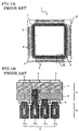
- Figs. 1A and 1B illustrate a conventional LSI chip.
- Fig. 1A is a top plan view of the same, and
- Fig. 1B is an enlarged view of an area M in Fig. 1A.
- LSI chip 1 is comprised of an inner area 2 located centrally at a surface of LSI chip 1, an input/output area 3 located around the inner area 2, and a pad area 4 located around the input/output area 3.
- a plurality of input/output terminal 5 is arranged surrounding the inner area 2.
- a plurality of pads 6 is arranged surrounding the input/output area 3.
- first wire 7 in the form of a square, surrounding the inner area 2, and a second wire 8 in the form of a square, surrounding the first wire 7.
- the first wire 7 is electrically connected to a voltage source (not illustrated), and the second wire 8 is grounded.
- any wiring layers are not formed below the pads 6 in the pad area 4. This is because if wiring layers are formed below the pads 6, a force may be exerted on the pads 6 in a step of wire-bonding, resulting in that the pads 6 may be damaged.
- the pads 6 are electrically connected to the input/output terminal 5, the first wire 7 or the second wire 8 through a via contact 9.
- a pad 6 electrically connected to the input/output terminal 5 is called a signal pad 6a
- a pad 6 electrically connected to the first wire 7 is called a VDD pad 6b
- a pad 6 electrically connected to the second wire 8 is called a GND pad 6c.
- Each of the first and second wires 7 and 8 is comprised of a plurality of metal wire layers in a multi-layered structure in the input/output area 3.
- the first wire 7 is formed just above a p-channel region in an input/output buffer
- the second wire 8 is formed separately from the first wire 7 just above a n-channel region in an input/output buffer.
- the first and second wires 7 and 8 are not designed to have a structure suitable for defining a bypass capacitor therein for suppressing noises in a power source line to thereby stabilize a voltage. Accordingly, in order to ensure a resistance to such noises and an operation at a high rate, it would be necessary to form quite a lot of the VDD pads 6b and the GND pads 6c.
- a bypass capacitor is often formed around a chip on a substrate.
- such a bypass capacitor formed on a substrate would be a bar to an increase in a density at which components are mounted on a substrate.
- Japanese Unexamined Patent Publication No. 5-55380 has suggested a semiconductor integrated circuit device including a plurality of wiring layers, characterized in that a first wiring layer electrically connected to a voltage source is formed all over at least one of the wiring layers, and that a second wiring layer grounded is formed all over at least one of said wiring layers except the first wiring layer.
- Japanese Unexamined Patent Publication No. 9-307067 has suggested a semi-custom semiconductor integrated circuit device including a capacitor formed in a non-used bonding pad area.
- the capacitor has at least three wiring layers and insulating layers sandwiched between wiring layers. A first voltage is applied to a lower wiring layer, a second voltage is applied to an intermediate wiring layer, and the first voltage or a third voltage is applied to an upper wiring layer.
- a semiconductor device having a plurality of wiring layers in a multi-layered structure, the semiconductor device including an inner area at a surface and a pad area surrounding the inner area therein, characterized in that the semiconductor device includes a device fabricated below the pad area.
- a method of fabricating a semiconductor device having a plurality of wiring layers in a multi-layered structure, and having an inner area at a surface and a pad area surrounding the inner area therein including the steps of (a) forming the inner area, and (b) fabricating a device below the pad area, the steps (a) and (b) being to be concurrently carried out.
- a device is fabricated below the pad area. Accordingly, a device such as a bypass capacitor can be fabricated without occupying a space. The thus fabricated bypass capacitor would enhance a resistance to noises and a radio-frequency characteristic in a power source line without increasing pads in number.
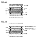
- Figs. 2A, 2B, 3A and 3B illustrate a LSI chip 10 as a semiconductor device in accordance with the first embodiment of the present invention.
- Fig. 2A is a top plan view of the LSI chip 10
- Fig. 2B is an enlarged view of the area A in Fig. 2A
- Fig. 3A is a cross-sectional view taken along the line B-B in Fig. 2B
- Fig. 3B is a cross-sectional view taken along the line C-C in Fig. 2B
- the LSI chip 10 includes a plurality of wiring layers in a multi-layered structure. As illustrated in Fig. 2A, the LSI chip 10 is comprised of an inner area 11 located centrally at a surface of the LSI chip 10, an input/output area 12 located around the inner area 11, and a pad area 13 located around the input/output area 12.
- a plurality of input/output terminal 14 are arranged in a square pattern, surrounding the inner area 11.
- a plurality of pads 15 are arranged in a square pattern, surrounding the input/output area 12.
- first wire 16a in a square pattern, surrounding the inner area 11, and a second wire 17a in a square pattern, surrounding the first wire 16a.
- the first wire 16a is electrically connected to a voltage source (not illustrated), and the second wire 17a is grounded.
- the first wire 16a is called the VDD wire 16a
- the second wire 17a is called GND wire 17a hereinafter.
- first wire 16b in a square pattern, surrounding the inner area 11, and a second wire 17b in a square pattern, surrounding the first wire 16b.
- the first wire 16b is electrically connected to a voltage source (not illustrated), and the second wire 17b is grounded.
- the first wire 16b is called the VDD wire 16b
- the second wire 17b is called GND wire 17b hereinafter.
- the pads 15 are electrically connected to the input/output terminal 14, the VDD wire 16b or the GND wire 17b through a via contact 18.
- a pad 15 electrically connected to the input/output terminal 14 is called a signal pad 15a
- a pad 15 electrically connected to the VDD wire 16b is called a VDD pad 15b
- a pad 15 electrically connected to the second wire 17b is called a GND pad 15c.
- the VDD wire 16b in the pad area 13 is comprised of a plurality of first metal wiring layers 16 in a multi-layered structure.
- the first metal wiring layers 16 are electrically connected to one another through via contacts 18 formed through first interlayer insulating films 16c sandwiched between the first metal wiring layers 16.
- the GND wire 17b in the pad area 13 is comprised of a plurality of second metal wiring layers 17 in a multi-layered structure.
- the second metal wiring layers 17 are electrically connected to one another through via contacts 18 formed through the first interlayer insulating films 16c.
- Each of the first metal wiring layers 16 and each of the second metal wiring layers 17 are formed in the same layer, and separated away from each other.
- the VDD wire 16a in the input/output area 12 has the same structure as that of the VDD wire 16b in the pad area 13.
- the VDD wire 16a is comprised of a plurality of first metal wiring layers 16 in a multi-layered structure.
- the first metal wiring layers 16 are electrically connected to one another through via contacts 18 formed through first interlayer insulating films 16c sandwiched between the first metal wiring layers 16.
- the GND wire 17a in the input/output area 12 has the same structure as that of the VDD wire 17b in the pad area 13. Specifically, the GND wire 17a in the input/output area 12 is comprised of a plurality of second metal wiring layers 17 in a multi-layered structure. The second metal wiring layers 17 are electrically connected to one another through via contacts 18 formed through the first interlayer insulating films 16c.
- Each of the first metal wiring layers 16 and each of the second metal wiring layers 17 are formed in the same layer, and separated away from each other.
- the VDD wire 16b in the pad area 13 is electrically connected to the VDD wire 16a in the input/output area 12
- the GND wire 17b in the pad area 13 is electrically connected to the GND wire 17a in the input/output area 12.
- the LSI chip 10 in accordance with the first embodiment is designed to include the VDD wire 16a and the GND wire 17a in the input/output area 12, and the VDD wire 16b and the GND wire 17b in the pad area 13, and further include not only a bypass capacitor defined in the input/output area 12, but also a bypass capacitor defined by non-used metal wiring layers located below the pads 15 in the pad area 13.
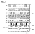
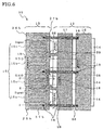
- Fig. 4 is a cross-sectional view illustrating a portion of the LSI chip 10 located below the pad 15, and Fig. 5 is a cross-sectional view illustrating an inner structure of the LSI chip 10.
- the LSI chip 10 includes a substrate 20, a transistor 22 formed on the substrate 20, and a wiring section 21 formed above the transistor 22 in the inner area 11.
- the transistor 22 is comprised of a p-channel transistor fabricated on a n-well 22a formed at a surface of the substrate 20, and a n-channel transistor fabricated on a p-well 22b formed at a surface of the substrate 20.
- the wiring section 21 is comprised of eight metal wiring layers M0 to M7, and interlayer insulating layers sandwiched between the metal wiring layers M0 to M7.
- the seven metal wiring layers M0 to M6 are formed on the substrate 20 below the pad 15 in order to define a bypass capacitor 19 in the pad area 13.
- the wiring section 21 is comprised of eighth metal wiring layers M0 to M7.
- the number of the metal wiring layers formed in the pad area 13 is equal to the number of the metal wiring layers defining the wiring section 21 to be formed in the inner area 11.
- the metal wiring layers M0 to M7 in the inner area 11 can be concurrently formed, resulting in that it is no longer necessary to form the metal wiring layers M0 to M7 in the pad area 13 separately from the metal wiring layers M0 to M7 to be formed in the inner area 11.
- the number of fabrication steps is not increased in order to define the bypass capacitor in the pad area 13, even if the bypass capacitor 19 is formed in the pad area 13, the number of steps for fabricating the LSI chip 10 remains the same as the number of steps for fabricating the LSI chip 10 without the bypass capacitor 19.
- the bypass capacitor 19 is fabricated in the pad area 13 which was a dead space, ensuring enhancement in a resistance to noises and also in a radio-frequency characteristic in a power source line without newly preparing a space for forming a bypass capacitor therein.
- the bypass capacitor 19 having the above-mentioned structure further has a function of a power source line
- the LSI chip 10 could have an enhanced resistance to electromigration and IR drop.
- the LSI chip 10 in accordance with the first embodiment makes it no longer necessary to increase power source pads and ground pads in number unlike the conventional LSI chip, ensuring reduction in the number of pads to be added.
- a bypass capacitor is generally mounted on a substrate around a chip.
- the LSI chip 10 in accordance with the first embodiment makes it possible to increase a density at which components are mounted on a substrate. This is because a bypass capacitor is constituted of a power source line in a dead space in the pad area 13 in accordance with the first embodiment.
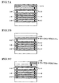
- Fig. 6 is a partial top plan view of a LSI chip 25 in accordance with the second embodiment of the present invention.
- Fig. 7A is a cross-sectional view taken along the line D-D in Fig. 6
- Fig. 7B is a cross-sectional view taken along the line E-E in Fig. 6.
- Fig. 7C is a cross-sectional view taken along the line F-F in Fig. 6.
- the LSI chip 25 in accordance with the second embodiment has the same structure as the structure of the LSI chip 10 except that the LSI chip 25 is designed to include a VDD wire 26a and a GND wire 27a in place of the VDD wire 16a and the GND wire 17a, and further include a VDD wire 26b and a GND wire 27b in place of the VDD wire 16b and the GND wire 17b.
- the VDD wire 26b is comprised of a first comb-shaped wire being electrically connected to a voltage source
- the GND wire 27b is comprised of a second comb-shaped wire being grounded.
- the VDD wires 26a and the GND 27b are arranged such that teeth of the first comb-shaped wire are located between teeth of the second comb-shaped wire in the same plane.
- the VDD wire 26a has the same structure as that of the VDD wire 26b, and the GND wire 27a has the same structure as that of the VDD wire 27b.
- a positional relationship between the VDD wire 26a and the GND wire 27a is identical to the positional relationship between the VDD wire 26b and the GND wire 27b.
- the VDD wire 26b formed in the pad area 13 is electrically connected to the VDD wire 26a formed in the input/output area 12 through a first electrical connector 28.
- the GND wire 27b formed in the pad area 13 is electrically connected to the GND wire 27a formed in the input/output area 12 through a second electrical connector 29.
- the LSI chip 25 in accordance with the second embodiment is designed to include the VDD wire 26a and the GND wire 27a in the input/output area 12, and the VDD wire 26b and the GND wire 27b in the pad area 13, and further include not only a bypass capacitor defined in the input/output area 12, but also a bypass capacitor defined by non-used metal wiring layers located below the pads 15 in the pad area 13.
- the bypass capacitor could have an increased capacity, because an additional capacity is defined between the teeth of the VDD wire 26a and teeth of the GND wire 27a, and further between the teeth of the VDD wire 26b and teeth of the GND wire 27b.
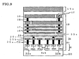
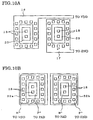
- Figs. 8A, 8B, 9, 10A and 10B illustrate a LSI chip 30 in accordance with the third embodiment.
- Fig. 8A is a top plan view of the LSI chip 30
- Fig. 8B is a partial circuit diagram of the LSI chip 30
- Fig. 9 is a cross-sectional view taken along the line G-G in Fig. 8A
- Fig. 10A is a plan view of the section H in Fig. 9
- Fig. 10B is a plan view of the section I in Fig. 9.
- the LSI chip 30 in accordance with the third embodiment is designed to include not only a bypass capacitor 19 (see Fig. 9), but also a protection device 31 such as a diode (see Fig. 8B) below the signal pad 15a in the pad area 13.
- the LSI chip 30 has the same structure as the structure of the LSI chip 10 except additionally having the protection device 31.
- the bypass capacitor 19 in the third embodiment has the same structure as the structure of the bypass capacitor 19 in the first embodiment, illustrated in Fig. 3A or 3B.
- the protection device 13 is comprised of a substrate 20 formed at a surface with a n-type well 32a and a p-type well 32b, a first interlayer insulating film 20a formed on the substrate 20, a first layer 20b formed on the first interlayer insulating film 20a, a second interlayer insulating film 20c formed on the first layer 20b, and a second signal wiring layer 33 formed on the second interlayer insulating film 20c.
- the n-type well 32a is formed at a surface thereof with a heavily doped p-type region 32ab and heavily doped n-type regions 32aa
- the p-type well 32b is formed at a surface thereof with heavily doped p-type regions 32ba and a heavily doped n-type region 32bb.
- the first layer 20b includes the first metal wiring layers 16, the second metal wiring layers 17, and first signal wiring layers 33a.
- the first metal wiring layers 16 are electrically connected to the heavily doped n-type regions 32aa formed in the n-type well 32a through via contacts 18.
- the second metal wiring layers 17 are electrically connected to the heavily doped p-type regions 32ba formed in the p-type well 32b through via contacts 18.
- One of the first signal wiring layers 33 is electrically connected to the heavily doped p-type region 32ab formed in the p-type well 32a through a via contact 18, and the other is electrically connected to the heavily doped n-type region 32bb formed in the n-type well 32b through a via contact 18.
- the second signal wiring layer 33 is electrically connected to the first signal wiring layers 33a through via contacts 18 formed through the second interlayer insulating film 20c.
- the heavily doped n-type regions 32aa in the n-type well 32a are electrically connected to a source voltage (VDD) through the first metal wiring layer 16
- the heavily doped p-type region 32ab in the n-type well 32a is electrically connected to the signal pad 15a through the first and second signal wiring layers 33
- the heavily doped n-type region 32bb in the p-type well 32b is electrically connected to the signal pad 15a through the first and second signal wiring layers 33
- the heavily doped p-type regions 32ba in the p-type well 32b are electrically connected to a source voltage (VDD) through the second metal wiring layer 17.
- bypass capacitor 19 not only the bypass capacitor 19 but also the protection device 31 can be fabricated below the pad 15 in the pad area 13.
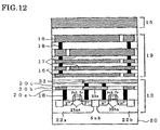
- Figs. 11 and 12 illustrate a LSI chip 35 in accordance with the fourth embodiment.
- Fig. 11 is a partial top plan view of the LSI chip 35
- Fig. 12 is a cross-sectional view taken along the line J-J in Fig. 11.
- the LSI chip 35 in accordance with the fourth embodiment is designed to include not only a bypass capacitor 19 (see Fig. 12), but also an extended portion of the input/output area 12 (see Figs. 11 and 12) below the signal pad 15a in the pad area 13.
- the LSI chip 35 has the same structure as the structure of the LSI chip 10 except additionally having the extended portion of the input/output area 12.
- the bypass capacitor 19 in the fourth embodiment has the same structure as the structure of the bypass capacitor 19 in the first embodiment, illustrated in Fig. 3A or 3B.
- bypass capacitor 19 is fabricated the extended portion of the input/output area 12.
- the extended portion of the input/output area 12 is comprised of a substrate 20 formed at a surface with a n-type well 22a and a p-type well 22b, a first interlayer insulating film 20a formed on the substrate 20, a first layer 20b formed on the first interlayer insulating film 20a, a second interlayer insulating film 20c formed on the first layer 20b, and a second signal wiring layer 33 formed on the second interlayer insulating film 20c.
- the n-type well 22a is formed at a surface thereof with a heavily doped p-type region 22aa
- the p-type well 22b is formed at a surface thereof with heavily doped n-type regions 22ba.
- the first layer 20b includes the first metal wiring layer 16, the second metal wiring layer 17, and a first signal wiring layer 33a.
- the first metal wiring layer 16 is electrically connected to the heavily doped p-type region 22aa formed in the n-type well 22a through a via contact 18.
- the second metal wiring layer 17 is electrically connected to the heavily doped n-type region 22ba formed in the p-type well 22b through a via contact 18.
- the first signal wiring layer 33a is electrically connected to both the heavily doped p-type region 22aa formed in the n-type well 22a and the heavily doped n-type region 22ba formed in the p-type well 22b through via contacts 18.
- the second signal wiring layer 33 is electrically connected to the first signal wiring layer 33a through via contacts 18 formed through the second interlayer insulating film 20c.
- the heavily doped p-type regions 22aa in the n-type well 22a are electrically connected to a source voltage (VDD) through the first metal wiring layer 16, and further to the signal pad 15a through the first and second signal wiring layers 33 and 33a.
- the heavily doped n-type regions 22ba in the p-type well 22b are electrically connected to the signal pad 15a through the first and second signal wiring layers 33 and 33a, and further to a source voltage (VDD) through the second metal wiring layer 17.
- the input/output area 12 can be fabricated below the pad 15 in the pad area 13. That is, the input/output area 12 can be extended such that an extended portion of the input/output area 12 is located below the signal pad 15a.
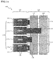
- Fig. 13 illustrates a LSI chip 40 in accordance with the fifth embodiment.
- the LSI chip 40 in accordance with the fifth embodiment is designed to include not only a bypass capacitor 19, but also both a protection device 31 such as a diode and an extended portion of the input/output area 12 below the signal pad 15a in the pad area 13.
- the LSI chip 40 has the same structure as the structure of the LSI chip 10 except additionally having both the protection device 31 and the extended portion of the input/output area 12.
- the bypass capacitor 19 in the fifth embodiment has the same structure as the structure of the bypass capacitor 19 in the first embodiment, illustrated in Fig. 3A or 3B.
- the protection device 31 in the fifth embodiment has the same structure as the structure of the protection device 31 in the third embodiment, illustrated in Figs. 8A, 8B, 9, 10A and 10B.
- the extended portion of the input/output area 12 in the fifth embodiment has the same structure as the structure of the extended portion of the input/output area 12 in the fourth embodiment, illustrated in Figs. 11 and 12.
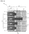
- Fig. 14 illustrates a LSI chip 45 in accordance with the sixth embodiment.
- Fig. 15 is a cross-sectional view taken along the line K-K in Fig. 14.
- the LSI chip 45 in accordance with the sixth embodiment is designed not to include a bypass capacitor 19, but designed to include only a protection device 31 such as a diode below the signal pad 15a in the pad area 13.
- the LSI chip 45 has the same structure as the structure of the LSI chip 10 except having the protection device 31 in place of the bypass capacitor 19.
- a plurality of signal wiring layers 33b in a multi-layered structure. Interlayer insulating layers are sandwiched between the signal wiring layers 33b. The signal wiring layers 33b are electrically connected to one another through via contacts 18 formed through the interlayer insulating layers.
- the protection device 31 in the sixth embodiment has the same structure as the structure of the protection device 31 in the third embodiment, illustrated in Figs. 8A, 8B, 9, 10A and 10B, except that the signal pad 15a is formed with via contacts 18 through which the signal pad 15a is electrically connected to the signal wiring layer 33b.
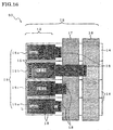
- Fig. 16 illustrates a LSI chip 50 in accordance with the seventh embodiment.
- Fig. 17 is a cross-sectional view taken along the line L-L in Fig. 16.
- the LSI chip 50 in accordance with the seventh embodiment is designed not to include a bypass capacitor 19, but designed to include only an extended portion of the input/output area 12 below the signal pad 15a in the pad area 13.
- the LSI chip 50 has the same structure as the structure of the LSI chip 10 except having the extended portion of the input/output area 12 in place of the bypass capacitor 19.
- a plurality of signal wiring layers 33c in a multi-layered structure. Interlayer insulating layers are sandwiched between the signal wiring layers 33c. The signal wiring layers 33c are electrically connected to one another through via contacts 18 formed through the interlayer insulating layers.
- the extended portion of the input/output area 12 in the seventh embodiment has the same structure as the structure of the extended portion of the input/output area 12 in the fourth embodiment, illustrated in Figs. 11 and 12, except that the signal pad 15a is formed with via contacts 18 through which the signal pad 15a is electrically connected to the signal wiring layer 33c.
- various devices such as the bypass capacitor 19, the protection device 31 and/or an input/output device defining the input/output area 12 can be fabricated in a dead space located below the pad area 13, for instance, a space located below the signal pad 15a.
- a space located below the pad 15 which space was not conventionally used because a device fabricated in such a space might be damaged in fabrication steps.
- the LSI chip may be fabricated by a packaging process in which components are assembled by compressive fitting, or a flip-chip process.
- the pads 15 are electrically connected any one of the input/output terminal 14, the VDD wire 16b or the GND wire 17b.
- the pads 15 may include pads which are electrically connected to none of the input/output terminal 14, the VDD wire 16b and the GND wire 17b.
- bypass capacitors may be formed in dependence on a specific power source, or a bypass capacitor may be formed only for an input/output power source emitting high noises through a power source line.
- the bypass capacitor may be designed to have a closed looped layout or a layout partially cut out.
Landscapes
- Semiconductor Integrated Circuits (AREA)
- Design And Manufacture Of Integrated Circuits (AREA)
- Internal Circuitry In Semiconductor Integrated Circuit Devices (AREA)
Abstract
Description
- The invention relates to a semiconductor device and a method of fabricating the same, and more particularly to a semiconductor device having a plurality of wiring layers in a multi-layered structure by which a bypass capacitor is defined, and a method of fabricating the same.
- There has been known a large scaled integrated circuit (LSI) chip as a semiconductor device including a plurality of wiring layers in a multi-layered structure, and including an inner area centrally at a surface and a pad area around the inner area.
- Figs. 1A and 1B illustrate a conventional LSI chip. Fig. 1A is a top plan view of the same, and Fig. 1B is an enlarged view of an area M in Fig. 1A.
- As illustrated in Fig. 1A,
LSI chip 1 is comprised of aninner area 2 located centrally at a surface ofLSI chip 1, an input/output area 3 located around theinner area 2, and apad area 4 located around the input/output area 3. - In the input/
output area 3, a plurality of input/output terminal 5 is arranged surrounding theinner area 2. In thepad area 4, a plurality ofpads 6 is arranged surrounding the input/output area 3. - In the input/
output area 3, there are formed afirst wire 7 in the form of a square, surrounding theinner area 2, and asecond wire 8 in the form of a square, surrounding thefirst wire 7. Thefirst wire 7 is electrically connected to a voltage source (not illustrated), and thesecond wire 8 is grounded. - Any wiring layers are not formed below the
pads 6 in thepad area 4. This is because if wiring layers are formed below thepads 6, a force may be exerted on thepads 6 in a step of wire-bonding, resulting in that thepads 6 may be damaged. - As illustrated in Fig. 1B, the
pads 6 are electrically connected to the input/output terminal 5, thefirst wire 7 or thesecond wire 8 through avia contact 9. Hereinbelow, apad 6 electrically connected to the input/output terminal 5 is called a signal pad 6a, apad 6 electrically connected to thefirst wire 7 is called a VDD pad 6b, and apad 6 electrically connected to thesecond wire 8 is called a GND pad 6c. - Each of the first and
second wires output area 3. In order to ensure to apply a source voltage to a transistor fabricated in the input/output area 3, thefirst wire 7 is formed just above a p-channel region in an input/output buffer, and thesecond wire 8 is formed separately from thefirst wire 7 just above a n-channel region in an input/output buffer. - However, the first and
second wires - This is because, with a size of a chip being smaller and smaller and an operation speed being higher and higher, it becomes more and more difficult for a conventional power source to guarantee a resistance to noises and a radio-frequency characteristic to be in an allowable range. Since it becomes difficult to reduce an impedance in a conventional power source in a chip fabricated smaller and smaller, it would be unavoidable to increase the VDD pads 6b and the GND pads 6c in order to ensure a high speed operation of a chip.
- A bypass capacitor is often formed around a chip on a substrate. However, such a bypass capacitor formed on a substrate would be a bar to an increase in a density at which components are mounted on a substrate.
- Japanese Unexamined Patent Publication No. 5-55380 has suggested a semiconductor integrated circuit device including a plurality of wiring layers, characterized in that a first wiring layer electrically connected to a voltage source is formed all over at least one of the wiring layers, and that a second wiring layer grounded is formed all over at least one of said wiring layers except the first wiring layer.
- Japanese Unexamined Patent Publication No. 9-307067 has suggested a semi-custom semiconductor integrated circuit device including a capacitor formed in a non-used bonding pad area. The capacitor has at least three wiring layers and insulating layers sandwiched between wiring layers. A first voltage is applied to a lower wiring layer, a second voltage is applied to an intermediate wiring layer, and the first voltage or a third voltage is applied to an upper wiring layer.
- However, the above-mentioned problems remain unsolved even in those Publications.
- In view of the above-mentioned problems in the conventional semiconductor devices, it is an object of the present invention to provide a semiconductor device which is capable of defining a bypass capacitor without occupying a space to thereby enhance a resistance to noises and a radio-frequency characteristic in a power source line without increasing pads in number.
- In one aspect of the present invention, there is provided a semiconductor device having a plurality of wiring layers in a multi-layered structure, the semiconductor device including an inner area at a surface and a pad area surrounding the inner area therein, characterized in that the semiconductor device includes a device fabricated below the pad area.
- In another aspect of the present invention, there is provided a method of fabricating a semiconductor device having a plurality of wiring layers in a multi-layered structure, and having an inner area at a surface and a pad area surrounding the inner area therein, the method including the steps of (a) forming the inner area, and (b) fabricating a device below the pad area, the steps (a) and (b) being to be concurrently carried out.
- The advantages obtained by the aforementioned present invention will be described hereinbelow.
- In the semiconductor device in accordance with the present invention, a device is fabricated below the pad area. Accordingly, a device such as a bypass capacitor can be fabricated without occupying a space. The thus fabricated bypass capacitor would enhance a resistance to noises and a radio-frequency characteristic in a power source line without increasing pads in number.
-
- Fig. 1A is a top plan view of a conventional LSI chip.
- Fig. 1B is an enlarged view of the area M in Fig. 1A.
- Fig. 2A is a top plan view of a semiconductor device in accordance with the first embodiment of the present invention.
- Fig. 2B is an enlarged view of the area A in Fig. 2A.
- Fig. 3A is a cross-sectional view taken along the line B-B in Fig. 2B.
- Fig. 3B is a cross-sectional view taken along the line C-C in Fig. 2B.
- Fig. 4 is a partial cross-sectional view of a semiconductor device.
- Fig. 5 is a partial cross-sectional view of a semiconductor device.
- Fig. 6 is a partial top plan view of a semiconductor device in accordance with the second embodiment of the present invention.
- Fig. 7A is a cross-sectional view taken along the line D-D in Fig. 6.
- Fig. 7B is a cross-sectional view taken along the line E-E in Fig. 6.
- Fig. 7C is a cross-sectional view taken along the line F-F in Fig. 6.
- Fig. 8A is a partial top plan view of a semiconductor device in accordance with the third embodiment of the present invention.
- Fig. 8B is a partial circuit diagram of the semiconductor device in accordance with the third embodiment of the present invention.
- Fig. 9 is a cross-sectional view taken along the line G-G in Fig. 8A.
- Fig. 10A is a plan view of the section H in Fig. 9.
- Fig. 10B is a plan view of the section I in Fig. 9.
- Fig. 11 is a partial top plan view of the semiconductor device in accordance with the fourth embodiment of the present invention.
- Fig. 12 is a cross-sectional view taken along the line J-J in Fig. 11.
- Fig. 13 is a partial top plan view of the semiconductor device in accordance with the fifth embodiment of the present invention.
- Fig. 14 is a partial top plan view of the semiconductor device in accordance with the sixth embodiment of the present invention.
- Fig. 15 is a cross-sectional view taken along the line K-K in Fig. 14.
- Fig. 16 is a partial top plan view of the semiconductor device in accordance with the seventh embodiment of the present invention.
- Fig. 17 is a cross-sectional view taken along the line L-L in Fig. 16.
-
- Figs. 2A, 2B, 3A and 3B illustrate a
LSI chip 10 as a semiconductor device in accordance with the first embodiment of the present invention. Fig. 2A is a top plan view of theLSI chip 10, Fig. 2B is an enlarged view of the area A in Fig. 2A, Fig. 3A is a cross-sectional view taken along the line B-B in Fig. 2B, and Fig. 3B is a cross-sectional view taken along the line C-C in Fig. 2B - The
LSI chip 10 includes a plurality of wiring layers in a multi-layered structure. As illustrated in Fig. 2A, theLSI chip 10 is comprised of an inner area 11 located centrally at a surface of theLSI chip 10, an input/output area 12 located around the inner area 11, and apad area 13 located around the input/output area 12. - In the input/
output area 12, a plurality of input/output terminal 14 are arranged in a square pattern, surrounding the inner area 11. In thepad area 13, a plurality ofpads 15 are arranged in a square pattern, surrounding the input/output area 12. - In the input/
output area 12, there are formed a first wire 16a in a square pattern, surrounding the inner area 11, and asecond wire 17a in a square pattern, surrounding the first wire 16a. The first wire 16a is electrically connected to a voltage source (not illustrated), and thesecond wire 17a is grounded. Hence, the first wire 16a is called the VDD wire 16a, and thesecond wire 17a is calledGND wire 17a hereinafter. - In the
pad area 13, there are formed afirst wire 16b in a square pattern, surrounding the inner area 11, and a second wire 17b in a square pattern, surrounding thefirst wire 16b. Thefirst wire 16b is electrically connected to a voltage source (not illustrated), and the second wire 17b is grounded. Hence, thefirst wire 16b is called theVDD wire 16b, and the second wire 17b is called GND wire 17b hereinafter. - As illustrated in Fig. 2B, the
pads 15 are electrically connected to the input/output terminal 14, theVDD wire 16b or the GND wire 17b through a viacontact 18. Hereinbelow, apad 15 electrically connected to the input/output terminal 14 is called asignal pad 15a, apad 15 electrically connected to theVDD wire 16b is called aVDD pad 15b, and apad 15 electrically connected to the second wire 17b is called aGND pad 15c. - As illustrated in Figs. 3A and 3B, the
VDD wire 16b in thepad area 13 is comprised of a plurality of first metal wiring layers 16 in a multi-layered structure. The first metal wiring layers 16 are electrically connected to one another through viacontacts 18 formed through first interlayer insulating films 16c sandwiched between the first metal wiring layers 16. - Similarly, the GND wire 17b in the
pad area 13 is comprised of a plurality of second metal wiring layers 17 in a multi-layered structure. The second metal wiring layers 17 are electrically connected to one another through viacontacts 18 formed through the first interlayer insulating films 16c. - Each of the first metal wiring layers 16 and each of the second metal wiring layers 17 are formed in the same layer, and separated away from each other.
- Vertically overlapping first and second metal wiring layers 16 and 17 with one of the first interlayer insulating films 16c being sandwiched therebetween define a bypass capacitor.
- Though not illustrated, the VDD wire 16a in the input/
output area 12 has the same structure as that of theVDD wire 16b in thepad area 13. Specifically, the VDD wire 16a is comprised of a plurality of first metal wiring layers 16 in a multi-layered structure. The first metal wiring layers 16 are electrically connected to one another through viacontacts 18 formed through first interlayer insulating films 16c sandwiched between the first metal wiring layers 16. - The
GND wire 17a in the input/output area 12 has the same structure as that of the VDD wire 17b in thepad area 13. Specifically, theGND wire 17a in the input/output area 12 is comprised of a plurality of second metal wiring layers 17 in a multi-layered structure. The second metal wiring layers 17 are electrically connected to one another through viacontacts 18 formed through the first interlayer insulating films 16c. - Each of the first metal wiring layers 16 and each of the second metal wiring layers 17 are formed in the same layer, and separated away from each other.
- Vertically overlapping first and second metal wiring layers 16 and 17 with one of the first interlayer insulating films 16c being sandwiched therebetween define a bypass capacitor.
- As illustrated in Fig. 3B, the
VDD wire 16b in thepad area 13 is electrically connected to the VDD wire 16a in the input/output area 12, and the GND wire 17b in thepad area 13 is electrically connected to theGND wire 17a in the input/output area 12. - As mentioned above, the
LSI chip 10 in accordance with the first embodiment is designed to include the VDD wire 16a and theGND wire 17a in the input/output area 12, and theVDD wire 16b and the GND wire 17b in thepad area 13, and further include not only a bypass capacitor defined in the input/output area 12, but also a bypass capacitor defined by non-used metal wiring layers located below thepads 15 in thepad area 13. - Fig. 4 is a cross-sectional view illustrating a portion of the
LSI chip 10 located below thepad 15, and Fig. 5 is a cross-sectional view illustrating an inner structure of theLSI chip 10. - As illustrated in Fig. 5, the
LSI chip 10 includes asubstrate 20, atransistor 22 formed on thesubstrate 20, and awiring section 21 formed above thetransistor 22 in the inner area 11. - The
transistor 22 is comprised of a p-channel transistor fabricated on a n-well 22a formed at a surface of thesubstrate 20, and a n-channel transistor fabricated on a p-well 22b formed at a surface of thesubstrate 20. - The
wiring section 21 is comprised of eight metal wiring layers M0 to M7, and interlayer insulating layers sandwiched between the metal wiring layers M0 to M7. - When the
LSI chip 10 is fabricated, as illustrated in Fig. 4, the seven metal wiring layers M0 to M6 are formed on thesubstrate 20 below thepad 15 in order to define abypass capacitor 19 in thepad area 13. - Namely, the seven metal wiring layers M0 to M6 and the
pad 15 as an eighth metal wiring layer M7, totally eight metal wiring layers M0 to M7, are formed in thepad area 13. - As mentioned earlier, the
wiring section 21 is comprised of eighth metal wiring layers M0 to M7. Thus, the number of the metal wiring layers formed in thepad area 13 is equal to the number of the metal wiring layers defining thewiring section 21 to be formed in the inner area 11. - Thus, when the
LSI chip 10 is fabricated, the metal wiring layers M0 to M7 in the inner area 11 (see Fig. 5) and the metal wiring layers M0 to M7 in the pad area (see Fig. 4) can be concurrently formed, resulting in that it is no longer necessary to form the metal wiring layers M0 to M7 in thepad area 13 separately from the metal wiring layers M0 to M7 to be formed in the inner area 11. Hence, since the number of fabrication steps is not increased in order to define the bypass capacitor in thepad area 13, even if thebypass capacitor 19 is formed in thepad area 13, the number of steps for fabricating theLSI chip 10 remains the same as the number of steps for fabricating theLSI chip 10 without thebypass capacitor 19. - As explained so far, in accordance with the first embodiment, the
bypass capacitor 19 is fabricated in thepad area 13 which was a dead space, ensuring enhancement in a resistance to noises and also in a radio-frequency characteristic in a power source line without newly preparing a space for forming a bypass capacitor therein. - In addition, since the
bypass capacitor 19 having the above-mentioned structure further has a function of a power source line, theLSI chip 10 could have an enhanced resistance to electromigration and IR drop. - As a result, the
LSI chip 10 in accordance with the first embodiment makes it no longer necessary to increase power source pads and ground pads in number unlike the conventional LSI chip, ensuring reduction in the number of pads to be added. - A bypass capacitor is generally mounted on a substrate around a chip. However, by forming at least a part of a bypass capacitor in a chip, the
LSI chip 10 in accordance with the first embodiment makes it possible to increase a density at which components are mounted on a substrate. This is because a bypass capacitor is constituted of a power source line in a dead space in thepad area 13 in accordance with the first embodiment. - Fig. 6 is a partial top plan view of a
LSI chip 25 in accordance with the second embodiment of the present invention. Fig. 7A is a cross-sectional view taken along the line D-D in Fig. 6, Fig. 7B is a cross-sectional view taken along the line E-E in Fig. 6., and Fig. 7C is a cross-sectional view taken along the line F-F in Fig. 6. - The
LSI chip 25 in accordance with the second embodiment has the same structure as the structure of theLSI chip 10 except that theLSI chip 25 is designed to include aVDD wire 26a and aGND wire 27a in place of the VDD wire 16a and theGND wire 17a, and further include a VDD wire 26b and a GND wire 27b in place of theVDD wire 16b and the GND wire 17b. - As illustrated in Fig. 6, the VDD wire 26b is comprised of a first comb-shaped wire being electrically connected to a voltage source, and the GND wire 27b is comprised of a second comb-shaped wire being grounded. The
VDD wires 26a and the GND 27b are arranged such that teeth of the first comb-shaped wire are located between teeth of the second comb-shaped wire in the same plane. - The
VDD wire 26a has the same structure as that of the VDD wire 26b, and theGND wire 27a has the same structure as that of the VDD wire 27b. A positional relationship between theVDD wire 26a and theGND wire 27a is identical to the positional relationship between the VDD wire 26b and the GND wire 27b. - As illustrated in Fig. 7B, the VDD wire 26b formed in the
pad area 13 is electrically connected to theVDD wire 26a formed in the input/output area 12 through a firstelectrical connector 28. Similarly, as illustrated in Fig. 7C, the GND wire 27b formed in thepad area 13 is electrically connected to theGND wire 27a formed in the input/output area 12 through a secondelectrical connector 29. - As mentioned above, the
LSI chip 25 in accordance with the second embodiment is designed to include theVDD wire 26a and theGND wire 27a in the input/output area 12, and the VDD wire 26b and the GND wire 27b in thepad area 13, and further include not only a bypass capacitor defined in the input/output area 12, but also a bypass capacitor defined by non-used metal wiring layers located below thepads 15 in thepad area 13. - In accordance with the second embodiment, the bypass capacitor could have an increased capacity, because an additional capacity is defined between the teeth of the
VDD wire 26a and teeth of theGND wire 27a, and further between the teeth of the VDD wire 26b and teeth of the GND wire 27b. - Figs. 8A, 8B, 9, 10A and 10B illustrate a
LSI chip 30 in accordance with the third embodiment. Fig. 8A is a top plan view of theLSI chip 30, Fig. 8B is a partial circuit diagram of theLSI chip 30, Fig. 9 is a cross-sectional view taken along the line G-G in Fig. 8A, Fig. 10A is a plan view of the section H in Fig. 9, and Fig. 10B is a plan view of the section I in Fig. 9. - As illustrated in Fig. 8A, the
LSI chip 30 in accordance with the third embodiment is designed to include not only a bypass capacitor 19 (see Fig. 9), but also aprotection device 31 such as a diode (see Fig. 8B) below thesignal pad 15a in thepad area 13. TheLSI chip 30 has the same structure as the structure of theLSI chip 10 except additionally having theprotection device 31. - The
bypass capacitor 19 in the third embodiment has the same structure as the structure of thebypass capacitor 19 in the first embodiment, illustrated in Fig. 3A or 3B. - As illustrated in Fig. 9, below the
bypass capacitor 19 is fabricated theprotection device 31. - The
protection device 13 is comprised of asubstrate 20 formed at a surface with a n-type well 32a and a p-type well 32b, a first interlayer insulating film 20a formed on thesubstrate 20, a first layer 20b formed on the first interlayer insulating film 20a, a second interlayer insulating film 20c formed on the first layer 20b, and a secondsignal wiring layer 33 formed on the second interlayer insulating film 20c. - The n-type well 32a is formed at a surface thereof with a heavily doped p-type region 32ab and heavily doped n-type regions 32aa, and the p-
type well 32b is formed at a surface thereof with heavily doped p-type regions 32ba and a heavily doped n-type region 32bb. - The first layer 20b includes the first metal wiring layers 16, the second metal wiring layers 17, and first
signal wiring layers 33a. The first metal wiring layers 16 are electrically connected to the heavily doped n-type regions 32aa formed in the n-type well 32a through viacontacts 18. The second metal wiring layers 17 are electrically connected to the heavily doped p-type regions 32ba formed in the p-type well 32b through viacontacts 18. One of the first signal wiring layers 33 is electrically connected to the heavily doped p-type region 32ab formed in the p-type well 32a through a viacontact 18, and the other is electrically connected to the heavily doped n-type region 32bb formed in the n-type well 32b through a viacontact 18. - The second
signal wiring layer 33 is electrically connected to the first signal wiring layers 33a through viacontacts 18 formed through the second interlayer insulating film 20c. - As illustrated in Fig. 10A, the heavily doped n-type regions 32aa in the n-type well 32a are electrically connected to a source voltage (VDD) through the first
metal wiring layer 16, the heavily doped p-type region 32ab in the n-type well 32a is electrically connected to thesignal pad 15a through the first and second signal wiring layers 33, the heavily doped n-type region 32bb in the p-type well 32b is electrically connected to thesignal pad 15a through the first and second signal wiring layers 33, and the heavily doped p-type regions 32ba in the p-type well 32b are electrically connected to a source voltage (VDD) through the secondmetal wiring layer 17. - As mentioned above, not only the
bypass capacitor 19 but also theprotection device 31 can be fabricated below thepad 15 in thepad area 13. - Figs. 11 and 12 illustrate a
LSI chip 35 in accordance with the fourth embodiment. Fig. 11 is a partial top plan view of theLSI chip 35, and Fig. 12 is a cross-sectional view taken along the line J-J in Fig. 11. - As illustrated in Fig. 11, the
LSI chip 35 in accordance with the fourth embodiment is designed to include not only a bypass capacitor 19 (see Fig. 12), but also an extended portion of the input/output area 12 (see Figs. 11 and 12) below thesignal pad 15a in thepad area 13. TheLSI chip 35 has the same structure as the structure of theLSI chip 10 except additionally having the extended portion of the input/output area 12. - The
bypass capacitor 19 in the fourth embodiment has the same structure as the structure of thebypass capacitor 19 in the first embodiment, illustrated in Fig. 3A or 3B. - As illustrated in Fig. 12, below the
bypass capacitor 19 is fabricated the extended portion of the input/output area 12. - The extended portion of the input/
output area 12 is comprised of asubstrate 20 formed at a surface with a n-type well 22a and a p-type well 22b, a first interlayer insulating film 20a formed on thesubstrate 20, a first layer 20b formed on the first interlayer insulating film 20a, a second interlayer insulating film 20c formed on the first layer 20b, and a secondsignal wiring layer 33 formed on the second interlayer insulating film 20c. - The n-type well 22a is formed at a surface thereof with a heavily doped p-type region 22aa, and the p-
type well 22b is formed at a surface thereof with heavily doped n-type regions 22ba. - The first layer 20b includes the first
metal wiring layer 16, the secondmetal wiring layer 17, and a firstsignal wiring layer 33a. The firstmetal wiring layer 16 is electrically connected to the heavily doped p-type region 22aa formed in the n-type well 22a through a viacontact 18. The secondmetal wiring layer 17 is electrically connected to the heavily doped n-type region 22ba formed in the p-type well 22b through a viacontact 18. The firstsignal wiring layer 33a is electrically connected to both the heavily doped p-type region 22aa formed in the n-type well 22a and the heavily doped n-type region 22ba formed in the p-type well 22b through viacontacts 18. - The second
signal wiring layer 33 is electrically connected to the firstsignal wiring layer 33a through viacontacts 18 formed through the second interlayer insulating film 20c. - The heavily doped p-type regions 22aa in the n-type well 22a are electrically connected to a source voltage (VDD) through the first
metal wiring layer 16, and further to thesignal pad 15a through the first and second signal wiring layers 33 and 33a. The heavily doped n-type regions 22ba in the p-type well 22b are electrically connected to thesignal pad 15a through the first and second signal wiring layers 33 and 33a, and further to a source voltage (VDD) through the secondmetal wiring layer 17. - As mentioned above, not only the
bypass capacitor 19 but also the input/output area 12 can be fabricated below thepad 15 in thepad area 13. That is, the input/output area 12 can be extended such that an extended portion of the input/output area 12 is located below thesignal pad 15a. - Fig. 13 illustrates a
LSI chip 40 in accordance with the fifth embodiment. - As illustrated in Fig. 13, the
LSI chip 40 in accordance with the fifth embodiment is designed to include not only abypass capacitor 19, but also both aprotection device 31 such as a diode and an extended portion of the input/output area 12 below thesignal pad 15a in thepad area 13. TheLSI chip 40 has the same structure as the structure of theLSI chip 10 except additionally having both theprotection device 31 and the extended portion of the input/output area 12. - The
bypass capacitor 19 in the fifth embodiment has the same structure as the structure of thebypass capacitor 19 in the first embodiment, illustrated in Fig. 3A or 3B. - The
protection device 31 in the fifth embodiment has the same structure as the structure of theprotection device 31 in the third embodiment, illustrated in Figs. 8A, 8B, 9, 10A and 10B. - The extended portion of the input/
output area 12 in the fifth embodiment has the same structure as the structure of the extended portion of the input/output area 12 in the fourth embodiment, illustrated in Figs. 11 and 12. - Fig. 14 illustrates a
LSI chip 45 in accordance with the sixth embodiment. Fig. 15 is a cross-sectional view taken along the line K-K in Fig. 14. - As illustrated in Figs. 14 and 15, the
LSI chip 45 in accordance with the sixth embodiment is designed not to include abypass capacitor 19, but designed to include only aprotection device 31 such as a diode below thesignal pad 15a in thepad area 13. TheLSI chip 45 has the same structure as the structure of theLSI chip 10 except having theprotection device 31 in place of thebypass capacitor 19. - As illustrated in Fig. 15, below the
signal pad 15a is formed a plurality of signal wiring layers 33b in a multi-layered structure. Interlayer insulating layers are sandwiched between the signal wiring layers 33b. The signal wiring layers 33b are electrically connected to one another through viacontacts 18 formed through the interlayer insulating layers. - The
protection device 31 in the sixth embodiment has the same structure as the structure of theprotection device 31 in the third embodiment, illustrated in Figs. 8A, 8B, 9, 10A and 10B, except that thesignal pad 15a is formed with viacontacts 18 through which thesignal pad 15a is electrically connected to the signal wiring layer 33b. - Fig. 16 illustrates a
LSI chip 50 in accordance with the seventh embodiment. Fig. 17 is a cross-sectional view taken along the line L-L in Fig. 16. - As illustrated in Figs. 16 and 17, the
LSI chip 50 in accordance with the seventh embodiment is designed not to include abypass capacitor 19, but designed to include only an extended portion of the input/output area 12 below thesignal pad 15a in thepad area 13. TheLSI chip 50 has the same structure as the structure of theLSI chip 10 except having the extended portion of the input/output area 12 in place of thebypass capacitor 19. - As illustrated in Fig. 17, below the
signal pad 15a is formed a plurality of signal wiring layers 33c in a multi-layered structure. Interlayer insulating layers are sandwiched between the signal wiring layers 33c. The signal wiring layers 33c are electrically connected to one another through viacontacts 18 formed through the interlayer insulating layers. - The extended portion of the input/
output area 12 in the seventh embodiment has the same structure as the structure of the extended portion of the input/output area 12 in the fourth embodiment, illustrated in Figs. 11 and 12, except that thesignal pad 15a is formed with viacontacts 18 through which thesignal pad 15a is electrically connected to the signal wiring layer 33c. - As mentioned earlier, in accordance with the above-mentioned first to seventh embodiments, various devices such as the
bypass capacitor 19, theprotection device 31 and/or an input/output device defining the input/output area 12 can be fabricated in a dead space located below thepad area 13, for instance, a space located below thesignal pad 15a. Thus, it is now possible to efficiently use a space located below thepad 15, which space was not conventionally used because a device fabricated in such a space might be damaged in fabrication steps. - In addition, those devices can be fabricated without an increase in the number of steps for fabricating the LSI chip in accordance with the above-mentioned embodiments. For instance, the LSI chip may be fabricated by a packaging process in which components are assembled by compressive fitting, or a flip-chip process.
- In the above-mentioned first to seventh embodiments, the
pads 15 are electrically connected any one of the input/output terminal 14, theVDD wire 16b or the GND wire 17b. However, thepads 15 may include pads which are electrically connected to none of the input/output terminal 14, theVDD wire 16b and the GND wire 17b. - Though the same bypass capacitor is formed in the above-mentioned first to seventh embodiments, various bypass capacitors may be formed in dependence on a specific power source, or a bypass capacitor may be formed only for an input/output power source emitting high noises through a power source line.
- The bypass capacitor may be designed to have a closed looped layout or a layout partially cut out.
Claims (21)
- A semiconductor device having a plurality of wiring layers in a multi-layered structure,
the semiconductor device including an inner area (11) at a surface and a pad area (13) surrounding the inner area (11) therein,
characterized in that the semiconductor device includes a device fabricated below the pad area (13). - The semiconductor device as set forth in claim 1, wherein the device is comprised of at least one of a bypass capacitor (19), a protection device (31), and an input/output device (12).
- The semiconductor device as set forth in claim 1, further comprising a second device fabricated below the device,the device being comprised of a bypass capacitor (19),the second device being comprised of at least one of a protection device (31) and an input/output device (12).
- The semiconductor device as set forth in claim 2, wherein the bypass capacitor (19) is comprised of metal wire layers (16, 17) arranged below the pad area (13).
- The semiconductor device as set forth in claim 4, wherein each of the metal wire layers (16, 17) is comprised of a first wire (16) and a second wire (17) with an interlayer insulating layer being sandwiched therebetween,the first wire (16) being electrically connected to a voltage source,the second wire (17) being grounded.
- The semiconductor device as set forth in claim 4, wherein each of the metal wire layers is comprised of a first comb-shaped wire (26) being electrically connected to a voltage source and a second comb-shaped wire (27) being grounded,
the first and second wires (26, 27) being arranged such that teeth of the first comb-shaped wire (26) are located between teeth of the second comb-shaped wire (27) in the same plane. - The semiconductor device as set forth in claim 5, further comprising at least one of first to fourth pads in the pad area (13),the first pad (15a) being electrically connected to the input/output device (12),the second pad (15b) being electrically connected to the first wire (16),the third pad being (15c) electrically connected to the second wire (17),the fourth pad being not electrically connected to the input/output device (12), the first wire (16) and the second wire (17).
- The semiconductor device as set forth in any one of claims 1 to 7, wherein the semiconductor device further includes an input/output area (12) between the inner area (11) and the pad area (13),the semiconductor device including a plurality of input/output terminals (14) in the input/output area (12), and a plurality of pads (15) in the pad area (13),the semiconductor device including (a) a first source voltage wire (16) being electrically connected to a voltage source and surrounding the inner area (11) in the pad area (13), and (b) a first ground wire (17) being grounded and surrounding the first source voltage wire in the pad area (13),each of the pads (15) being electrically connected to any one of the input/output terminals (14), the first source voltage wire (16), and the first ground wire (17),the first source voltage wire (16) being comprised of a plurality of first metal wiring layers in a multi-layered structure, the first metal wiring layers being electrically connected to one another through via-holes (18) formed through first interlayer insulating films sandwiched between the first metal wiring layers,the first ground wire (17) being comprised of a plurality of second metal wiring layers in a multi-layered structure, the second metal wiring layers being electrically connected to one another through via-holes (18) formed through the first interlayer insulating films,each of the first metal wiring layers and each of the second metal wiring layers being formed in the same layer,vertically adjacent first and second metal wiring layers with one of the first interlayer insulating films being sandwiched therebetween, among the first and second metal wiring layers, defining a bypass capacitor (19) as the device.
- The semiconductor device as set forth in claim 8, further comprising:the second source voltage wire (16) being comprised of a plurality of third metal wiring layers in a multi-layered structure, the third metal wiring layers being electrically connected to one another through via-holes (18) formed through second interlayer insulating films sandwiched between the third metal wiring layers,(c) a second source voltage wire (16) being electrically connected to a voltage source and surrounding the inner area (11) in the input/output area (12), and(d) a second ground wire (17) being grounded and surrounding the second source voltage wire in the input/output area (12),
the second ground wire (17) being comprised of a plurality of fourth metal wiring layers in a multi-layered structure, the fourth metal wiring layers being electrically connected to one another through via-holes (18) formed through the second interlayer insulating films,
each of the third metal wiring layers and each of the fourth metal wiring layers being formed in the same layer,
vertically adjacent third and fourth metal wiring layers with one of the second interlayer insulating films being sandwiched therebetween, among the third and fourth metal wiring layers, defining a bypass capacitor (19). - The semiconductor device as set forth in claim 9, wherein the first source voltage wire (16) is electrically connected to the second source voltage wire (16), and the first ground wire (17) is electrically connected to the second ground wire (17).
- The semiconductor device as set forth in claim 9, wherein the first source voltage wire is comprised of a first comb-shaped wire (26) being electrically connected to a voltage source, and the first ground wire is comprised of a second comb-shaped wire (27) being grounded,the second source voltage wire is comprised of a third comb-shaped wire (26) being electrically connected to a voltage source, and the second ground wire is comprised of a fourth comb-shaped wire (27) being grounded,the first and second wires being arranged such that teeth of the first comb-shaped wire (26) are located between teeth of the second comb-shaped wire (27) in the same plane,the third and fourth wires being arranged such that teeth of the third comb-shaped wire (26) are located between teeth of the fourth comb-shaped wire (27) in the same plane.
- The semiconductor device as set forth in claim 11, wherein the first source voltage wire is electrically connected to the second source voltage wire, and the first ground wire is electrically connected to the second ground wire.
- The semiconductor device as set forth in claim 8, further comprising a protection device (31) fabricated below the bypass capacitor (19),the protection device (31) comprising:(a) a substrate (20) formed at a surface with a first well (32a) having a first electrical conductivity and a second well (32b) having a second electrical conductivity;(b) a first interlayer insulating film (20a) formed on the substrate (20);(c) a first layer (20b) formed on the first interlayer insulating film (20a);(d) a second interlayer insulating film (20c) formed on the first layer (20b); and(e) a signal wiring layer (33a) formed on the second interlayer insulating film (20c),the first layer (20a) including one of the first metal wiring layers (16), one of the second metal wiring layers (17), and a second signal wiring layer (33) all electrically connected to the first or second well (32a, 32b) through via-holes (18) formed through the first interlayer insulating film (20a),the second signal wiring layer (33) being electrically connected to the signal wiring layer (33a) through via-holes (18) formed through the second interlayer insulating film (20c).
- The semiconductor device as set forth in claim 8, wherein the input/output area (12) has an extended portion located below the pad area (13),the extended portion comprising:(a) a substrate (20) formed at a surface with a first well (22a) having a first electrical conductivity and a second well (22b) having a second electrical conductivity;(b) a first interlayer insulating film (20a) formed on the substrate (20);(c) a first layer (20b) formed on the first interlayer insulating film (20a);(d) a second interlayer insulating film (20c) formed on the first layer (20b); and(e) a signal wiring layer (33) formed on second interlayer insulating film (20c),the first layer (20b) including one of the first metal wiring layers (16) electrically connected to the first well (22a) through a via-hole (18) formed through the first interlayer insulating film (20a), one of the second metal wiring layers (17) electrically connected to the second well (22b) through a via-hole (18) formed through the first interlayer insulating film (20a), and a second signal wiring layer (33) electrically connected to the first or second well (22a, 22b) through via-holes (18) formed through the first interlayer insulating film (20a),the second signal wiring layer (33) being electrically connected to the signal wiring layer (33a) through via-holes (18) formed through the second interlayer insulating film (20c).
- The semiconductor device as set forth in any one of claims 1 to 7, wherein the semiconductor device further includes an input/output area (12) between the inner area (11) and the pad area (13),the semiconductor device including a plurality of input/output terminals (14) in the input/output area (12), and a plurality of pads (15) in the pad area (13),the semiconductor device including a plurality of input/output terminals (14) in the input/output area (12), and a plurality of pads (15) in the pad area (13),the semiconductor device including (a) a first source voltage wire (16) being electrically connected to a voltage source and surrounding the inner area (11) in the pad area (13), and (b) a first ground wire (17) being grounded and surrounding the first source voltage wire in the pad area (13),each of the pads (15) being electrically connected to any one of the input/output terminals (14), the first source voltage wire (16), and the first ground wire (17),the semiconductor device including a protection device (31) as the device,the protection device (31) comprising:(a) a substrate (20) formed at a surface with a first well (32a) having a first electrical conductivity and a second well (32b) having a second electrical conductivity;(b) a first interlayer insulating film (20a) formed on the substrate (20);(c) a first layer (20b) formed on the first interlayer insulating film (20a);(d) a second interlayer insulating film (20c) formed on the first layer (20b); and(e) a signal wiring layer (33a) formed on the second interlayer insulating film (20c),the first layer (20a) including one of the first metal wiring layers (16), one of the second metal wiring layers (17), and a second signal wiring layer (33) all electrically connected to the first or second well (32a, 32b) through via-holes (18) formed through the first interlayer insulating film (20a),the second signal wiring layer (33) being electrically connected to the signal wiring layer (33a) through via-holes (18) formed through the second interlayer insulating film (20c).
- The semiconductor device as set forth in any one of claims 1 to 7, wherein the semiconductor device further includes an input/output area (12) between the inner area (11) and the pad area (13),the semiconductor device including a plurality of input/output terminals (14) in the input/output area (12), and a plurality of pads in the pad area (13),the semiconductor device including (a) a first source voltage wire (16) being electrically connected to a voltage source and surrounding the inner area (11) in the pad area (13), and (b) a first ground wire (17) being grounded and surrounding the first source voltage wire in the pad area (13),each of the pads being electrically connected to any one of the input/output terminals (14), the first source voltage wire (16), and the first ground wire (17),the input/output area (12) having an extended portion located below the pad area (13) as the device,the extended portion comprising:(a) a substrate (20) formed at a surface with a first well (22a) having a first electrical conductivity and a second well (22b) having a second electrical conductivity;(b) a first interlayer insulating film (20a) formed on the substrate (20);(c) a first layer (20b) formed on the first interlayer insulating film (20a);(d) a second interlayer insulating film (20c) formed on the first layer (20b); and(e) a signal wiring layer (33) formed on second interlayer insulating film (20c),the first layer (20b) including one of the first metal wiring layers (16) electrically connected to the first well (22a) through a via-hole (18) formed through the first interlayer insulating film (20a), one of the second metal wiring layers (17) electrically connected to the second well (22b) through a via-hole (18) formed through the first interlayer insulating film (20a), and a second signal wiring layer (33) electrically connected to the first or second well (22a, 22b) through via-holes (18) formed through the first interlayer insulating film (20a),the second signal wiring layer (33) being electrically connected to the signal wiring layer (33a) through via-holes (18) formed through the second interlayer insulating film (20c).
- A method of fabricating a semiconductor device having a plurality of wiring layers in a multi-layered structure, and having an inner area (11) at a surface and a pad area (13) surrounding the inner area (11) therein,the method comprising the steps of:(a) forming the inner area (11); and(b) fabricating a device (19, 31, 12) below the pad area (13),the steps (a) and (b) being to be concurrently carried out.
- The method as set forth in claim 17, wherein at least one of a bypass capacitor (19), a protection device (31), and an input/output device (12) is fabricated as the device in the step (b).
- The method as set forth in claim 17, further comprising the step of (c) fabricating a second device below the device.
- The method as set forth in claim 19, wherein the step (c) is carried out concurrently with the steps (a) and (b).
- The method as set forth in claim 19, wherein a bypass capacitor (19) is fabricated as the device in the step (b), and at least one of a protection device (31) and an input/output device (12) is fabricated as the second device in the step (c).
Applications Claiming Priority (2)
| Application Number | Priority Date | Filing Date | Title |
|---|---|---|---|
| JP2000100732A JP3727220B2 (en) | 2000-04-03 | 2000-04-03 | Semiconductor device |
| JP2000100732 | 2000-04-03 |
Publications (1)
| Publication Number | Publication Date |
|---|---|
| EP1143513A1 true EP1143513A1 (en) | 2001-10-10 |
Family
ID=18614891
Family Applications (1)
| Application Number | Title | Priority Date | Filing Date |
|---|---|---|---|
| EP01108319A Withdrawn EP1143513A1 (en) | 2000-04-03 | 2001-04-02 | Semiconductor device and method of fabricating the same |
Country Status (3)
| Country | Link |
|---|---|
| US (1) | US6781238B2 (en) |
| EP (1) | EP1143513A1 (en) |
| JP (1) | JP3727220B2 (en) |
Cited By (5)
| Publication number | Priority date | Publication date | Assignee | Title |
|---|---|---|---|---|
| WO2004004002A1 (en) * | 2002-07-01 | 2004-01-08 | Infineon Technologies Ag | Semiconductor structure integrated under a pad |
| WO2004040646A1 (en) * | 2002-10-22 | 2004-05-13 | Infineon Technologies Ag | Electronic component with an integrated passive electronic component and method for production thereof |
| FR2851060A1 (en) * | 2003-02-11 | 2004-08-13 | St Microelectronics Sa | CIRCUIT WITH INTEGRATED VOLTAGE REGULATOR AND MANUFACTURING METHOD THEREOF |
| FR2890783A1 (en) * | 2005-09-12 | 2007-03-16 | St Microelectronics | INTEGRATED ELECTRONIC CIRCUIT INCORPORATING A CAPACITOR |
| WO2008004151A3 (en) * | 2006-06-30 | 2008-03-06 | Nxp Bv | Power supply network |
Families Citing this family (42)
| Publication number | Priority date | Publication date | Assignee | Title |
|---|---|---|---|---|
| JP2003289104A (en) * | 2002-03-28 | 2003-10-10 | Ricoh Co Ltd | Semiconductor device protection circuit and semiconductor device |
| JP4258205B2 (en) * | 2002-11-11 | 2009-04-30 | パナソニック株式会社 | Semiconductor device |
| US20040226735A1 (en) * | 2003-05-12 | 2004-11-18 | Ping Wu | Method and apparatus for integrated noise decoupling |
| US7675174B2 (en) * | 2003-05-13 | 2010-03-09 | Stmicroelectronics, Inc. | Method and structure of a thick metal layer using multiple deposition chambers |
| JP2005057254A (en) * | 2003-07-18 | 2005-03-03 | Yamaha Corp | Semiconductor device |
| US7037820B2 (en) * | 2004-01-30 | 2006-05-02 | Agere Systems Inc. | Cross-fill pattern for metal fill levels, power supply filtering, and analog circuit shielding |
| JP4913329B2 (en) * | 2004-02-09 | 2012-04-11 | ルネサスエレクトロニクス株式会社 | Semiconductor device |
| JP2005243907A (en) | 2004-02-26 | 2005-09-08 | Renesas Technology Corp | Semiconductor device |
| JP2006019692A (en) * | 2004-06-03 | 2006-01-19 | Toshiba Corp | Semiconductor device |
| KR100615579B1 (en) * | 2004-09-20 | 2006-08-25 | 삼성전자주식회사 | Semiconductor memory device and power line arrangement method thereof |
| JP4682622B2 (en) * | 2005-01-11 | 2011-05-11 | セイコーエプソン株式会社 | Semiconductor device |
| KR100663360B1 (en) * | 2005-04-20 | 2007-01-02 | 삼성전자주식회사 | Semiconductor Devices Having Thin Film Transistors and Manufacturing Methods Thereof |
| KR100618903B1 (en) * | 2005-06-18 | 2006-09-01 | 삼성전자주식회사 | Semiconductor integrated circuit having independent power supply and semiconductor integrated circuit comprising semiconductor integrated circuit and method for forming semiconductor integrated circuit |
| JP2007012938A (en) * | 2005-06-30 | 2007-01-18 | Seiko Epson Corp | Integrated circuit device |
| JP5234239B2 (en) | 2005-07-06 | 2013-07-10 | セイコーエプソン株式会社 | Semiconductor device |
| JP4605378B2 (en) | 2005-07-13 | 2011-01-05 | セイコーエプソン株式会社 | Semiconductor device |
| JP2007027481A (en) | 2005-07-19 | 2007-02-01 | Seiko Epson Corp | Semiconductor device |
| JP2007036021A (en) * | 2005-07-28 | 2007-02-08 | Seiko Epson Corp | Semiconductor device |
| JP4995455B2 (en) | 2005-11-30 | 2012-08-08 | ルネサスエレクトロニクス株式会社 | Semiconductor device |
| JP5065606B2 (en) | 2006-03-03 | 2012-11-07 | ルネサスエレクトロニクス株式会社 | Semiconductor device |
| JP2006245596A (en) * | 2006-04-03 | 2006-09-14 | Ricoh Co Ltd | Semiconductor device |
| KR100773097B1 (en) * | 2006-08-22 | 2007-11-02 | 삼성전자주식회사 | Semiconductor device with pad |
| US20080079159A1 (en) * | 2006-10-02 | 2008-04-03 | Texas Instruments Incorporated | Focused stress relief using reinforcing elements |
| JP5190913B2 (en) * | 2007-01-15 | 2013-04-24 | ルネサスエレクトロニクス株式会社 | Semiconductor integrated circuit device |
| JP4522435B2 (en) * | 2007-06-05 | 2010-08-11 | 富士通テン株式会社 | High frequency circuit device and radar device |
| JP5590802B2 (en) | 2008-04-11 | 2014-09-17 | ピーエスフォー ルクスコ エスエイアールエル | Basic cell and semiconductor device |
| JP2010021412A (en) * | 2008-07-11 | 2010-01-28 | Oki Semiconductor Co Ltd | Semiconductor thyristor device |
| JPWO2010026956A1 (en) * | 2008-09-02 | 2012-02-02 | 日本電気株式会社 | Semiconductor device and manufacturing method thereof |
| JP5657264B2 (en) * | 2010-03-31 | 2015-01-21 | ラピスセミコンダクタ株式会社 | Semiconductor integrated circuit device |
| JP5621357B2 (en) * | 2010-06-30 | 2014-11-12 | 富士通セミコンダクター株式会社 | Semiconductor device |
| JP2010263234A (en) * | 2010-07-16 | 2010-11-18 | Renesas Electronics Corp | Semiconductor integrated circuit device |
| US8378491B2 (en) * | 2010-08-24 | 2013-02-19 | Infineon Technologies Ag | Integrated circuit including interconnect levels |
| JP5558336B2 (en) * | 2010-12-27 | 2014-07-23 | 株式会社東芝 | Semiconductor device |
| JP6054612B2 (en) * | 2012-03-06 | 2016-12-27 | ラピスセミコンダクタ株式会社 | Semiconductor integrated device |
| WO2017212644A1 (en) * | 2016-06-10 | 2017-12-14 | 株式会社ソシオネクスト | Semiconductor device |
| JP6790705B2 (en) * | 2016-10-13 | 2020-11-25 | セイコーエプソン株式会社 | Circuits, oscillators, electronics and mobiles |
| US12527000B2 (en) * | 2018-10-09 | 2026-01-13 | Micron Technology, Inc. | Methods of forming a device, and related devices, memory devices, and electronic systems |
| JP7268729B2 (en) | 2019-05-23 | 2023-05-08 | 株式会社ソシオネクスト | semiconductor equipment |
| WO2020235082A1 (en) | 2019-05-23 | 2020-11-26 | 株式会社ソシオネクスト | Semiconductor device |
| JP7200066B2 (en) * | 2019-08-22 | 2023-01-06 | ルネサスエレクトロニクス株式会社 | semiconductor equipment |
| WO2021090471A1 (en) * | 2019-11-08 | 2021-05-14 | 株式会社ソシオネクスト | Semiconductor integrated circuit device |
| CN114566483B (en) * | 2020-11-27 | 2025-02-18 | Oppo广东移动通信有限公司 | Chip and electronic device |
Citations (4)
| Publication number | Priority date | Publication date | Assignee | Title |
|---|---|---|---|---|
| JPS5923541A (en) * | 1982-07-30 | 1984-02-07 | Nec Corp | Semiconductor device |
| JPS61248540A (en) * | 1985-04-26 | 1986-11-05 | Mitsubishi Electric Corp | Input protective device |
| JPH04116851A (en) * | 1990-09-06 | 1992-04-17 | Toshiba Corp | Semiconductor integrated circuit element |
| EP0637840A1 (en) * | 1993-08-05 | 1995-02-08 | AT&T Corp. | Integrated circuit with active devices under bond pads |
Family Cites Families (16)
| Publication number | Priority date | Publication date | Assignee | Title |
|---|---|---|---|---|
| JPS61263251A (en) | 1985-05-17 | 1986-11-21 | Nec Corp | Semiconductor device |
| US4949150A (en) * | 1986-04-17 | 1990-08-14 | Exar Corporation | Programmable bonding pad with sandwiched silicon oxide and silicon nitride layers |
| JPH01109746A (en) | 1987-10-22 | 1989-04-26 | Mitsubishi Electric Corp | CMOS gate array |
| JPH02117138A (en) * | 1988-10-27 | 1990-05-01 | Matsushita Electron Corp | Semiconductor device |
| JPH02163960A (en) * | 1988-12-16 | 1990-06-25 | Toshiba Corp | Semiconductor device |
| JPH04196552A (en) * | 1990-11-28 | 1992-07-16 | Mitsubishi Electric Corp | Semiconductor device and manufacture thereof |
| JP3139783B2 (en) | 1991-08-22 | 2001-03-05 | 株式会社東芝 | Semiconductor integrated circuit device |
| JPH05136125A (en) * | 1991-11-14 | 1993-06-01 | Hitachi Ltd | Clock wiring and semiconductor integrated circuit device having clock wiring |
| JP3390875B2 (en) * | 1992-11-12 | 2003-03-31 | 日本テキサス・インスツルメンツ株式会社 | Semiconductor device |
| JP2570147B2 (en) * | 1993-11-18 | 1997-01-08 | 日本電気株式会社 | Semiconductor device |
| JP3432963B2 (en) * | 1995-06-15 | 2003-08-04 | 沖電気工業株式会社 | Semiconductor integrated circuit |
| US5903031A (en) * | 1995-07-04 | 1999-05-11 | Matsushita Electric Industrial Co., Ltd. | MIS device, method of manufacturing the same, and method of diagnosing the same |
| JPH09307067A (en) | 1996-05-16 | 1997-11-28 | Oki Electric Ind Co Ltd | Semi-custom semiconductor integrated circuit device |
| JPH10313095A (en) | 1997-05-13 | 1998-11-24 | Nec Corp | Semiconductor device |
| JPH1140765A (en) * | 1997-07-16 | 1999-02-12 | Toshiba Corp | Semiconductor memory device and method of manufacturing the same |
| JP3948822B2 (en) | 1998-04-21 | 2007-07-25 | ローム株式会社 | Semiconductor integrated circuit |
-
2000
- 2000-04-03 JP JP2000100732A patent/JP3727220B2/en not_active Expired - Fee Related
-
2001
- 2001-04-02 EP EP01108319A patent/EP1143513A1/en not_active Withdrawn
- 2001-04-03 US US09/823,752 patent/US6781238B2/en not_active Expired - Fee Related
Patent Citations (4)
| Publication number | Priority date | Publication date | Assignee | Title |
|---|---|---|---|---|
| JPS5923541A (en) * | 1982-07-30 | 1984-02-07 | Nec Corp | Semiconductor device |
| JPS61248540A (en) * | 1985-04-26 | 1986-11-05 | Mitsubishi Electric Corp | Input protective device |
| JPH04116851A (en) * | 1990-09-06 | 1992-04-17 | Toshiba Corp | Semiconductor integrated circuit element |
| EP0637840A1 (en) * | 1993-08-05 | 1995-02-08 | AT&T Corp. | Integrated circuit with active devices under bond pads |
Non-Patent Citations (3)
| Title |
|---|
| PATENT ABSTRACTS OF JAPAN vol. 008, no. 107 (E - 245) 19 May 1984 (1984-05-19) * |
| PATENT ABSTRACTS OF JAPAN vol. 011, no. 099 (E - 493) 27 March 1987 (1987-03-27) * |
| PATENT ABSTRACTS OF JAPAN vol. 016, no. 367 (E - 1245) 7 August 1992 (1992-08-07) * |
Cited By (11)
| Publication number | Priority date | Publication date | Assignee | Title |
|---|---|---|---|---|
| WO2004004002A1 (en) * | 2002-07-01 | 2004-01-08 | Infineon Technologies Ag | Semiconductor structure integrated under a pad |
| US7190077B2 (en) | 2002-07-01 | 2007-03-13 | Infineon Technologies Ag | Semiconductor structure integrated under a pad |
| CN100440497C (en) * | 2002-07-01 | 2008-12-03 | 因芬尼昂技术股份公司 | integrated semiconductor structure |
| WO2004040646A1 (en) * | 2002-10-22 | 2004-05-13 | Infineon Technologies Ag | Electronic component with an integrated passive electronic component and method for production thereof |
| US7193263B2 (en) | 2002-10-22 | 2007-03-20 | Infineon Technologies Ag | Electronic component having an integrated passive electronic component and associated production method |
| CN100459112C (en) * | 2002-10-22 | 2009-02-04 | 因芬尼昂技术股份公司 | Electronic assemblies with integrated passive electronic components |
| FR2851060A1 (en) * | 2003-02-11 | 2004-08-13 | St Microelectronics Sa | CIRCUIT WITH INTEGRATED VOLTAGE REGULATOR AND MANUFACTURING METHOD THEREOF |
| EP1450407A1 (en) * | 2003-02-11 | 2004-08-25 | STMicroelectronics S.A. | Integrated voltage regulating circuit and method of fabrication thereof |
| FR2890783A1 (en) * | 2005-09-12 | 2007-03-16 | St Microelectronics | INTEGRATED ELECTRONIC CIRCUIT INCORPORATING A CAPACITOR |
| WO2008004151A3 (en) * | 2006-06-30 | 2008-03-06 | Nxp Bv | Power supply network |
| US7928567B2 (en) | 2006-06-30 | 2011-04-19 | Nxp B.V. | Power supply network |
Also Published As
| Publication number | Publication date |
|---|---|
| JP2001284537A (en) | 2001-10-12 |
| US20010035555A1 (en) | 2001-11-01 |
| US6781238B2 (en) | 2004-08-24 |
| JP3727220B2 (en) | 2005-12-14 |
Similar Documents
| Publication | Publication Date | Title |
|---|---|---|
| EP1143513A1 (en) | Semiconductor device and method of fabricating the same | |
| US6809419B2 (en) | Semiconductor device | |
| USRE41668E1 (en) | Seal ring structure for radio frequency integrated circuits | |
| JP4995455B2 (en) | Semiconductor device | |
| US5514892A (en) | Electrostatic discharge protection device | |
| US7232705B2 (en) | Integrated circuit bond pad structures and methods of making | |
| US6858885B2 (en) | Semiconductor apparatus and protection circuit | |
| US8896129B2 (en) | Semiconductor device and manufacturing method for the same | |
| US20220336305A1 (en) | Semiconductor device having electrode pads arranged between groups of external electrodes | |
| US5300796A (en) | Semiconductor device having an internal cell array region and a peripheral region surrounding the internal cell array for providing input/output basic cells | |
| US6476459B2 (en) | Semiconductor integrated circuit device with capacitor formed under bonding pad | |
| US20080006930A1 (en) | Semiconductor package | |
| US20070222069A1 (en) | Semiconductor integrated circuit device | |
| CN205582918U (en) | Semiconductor device | |
| US5923048A (en) | Semiconductor integrated circuit device with test element | |
| JP2007059449A (en) | Semiconductor device | |
| JPH08236706A (en) | Semiconductor integrated circuit element and semiconductor device incorporating the element | |
| JP2001177056A (en) | Semiconductor integrated circuit device | |
| US5554881A (en) | Constitution of an electrode arrangement in a semiconductor element | |
| US6730946B2 (en) | Semiconductor device | |
| US6787928B1 (en) | Integrated circuit device having pads structure formed thereon and method for forming the same | |
| JPS62249467A (en) | Semiconductor integrated circuit device | |
| JP3441104B2 (en) | Semiconductor device | |
| JP2001156178A (en) | Semiconductor device and automatic layout method for the same | |
| JPH04130653A (en) | Resin sealing type semiconductor device |
Legal Events
| Date | Code | Title | Description |
|---|---|---|---|
| PUAI | Public reference made under article 153(3) epc to a published international application that has entered the european phase |
Free format text: ORIGINAL CODE: 0009012 |
|
| 17P | Request for examination filed |
Effective date: 20010725 |
|
| AK | Designated contracting states |
Kind code of ref document: A1 Designated state(s): DE Kind code of ref document: A1 Designated state(s): AT BE CH CY DE DK ES FI FR GB GR IE IT LI LU MC NL PT SE TR |
|
| AX | Request for extension of the european patent |
Free format text: AL;LT;LV;MK;RO;SI |
|
| AKX | Designation fees paid |
Free format text: DE |
|
| RAP1 | Party data changed (applicant data changed or rights of an application transferred) |
Owner name: NEC ELECTRONICS CORPORATION |
|
| 17Q | First examination report despatched |
Effective date: 20040702 |
|
| STAA | Information on the status of an ep patent application or granted ep patent |
Free format text: STATUS: THE APPLICATION HAS BEEN WITHDRAWN |
|
| 18W | Application withdrawn |
Effective date: 20060529 |