EP1146570A1 - Dispositif émetteur de lumière à semi-conducteur et methode pour la fabrication d'un support - Google Patents
Dispositif émetteur de lumière à semi-conducteur et methode pour la fabrication d'un support Download PDFInfo
- Publication number
- EP1146570A1 EP1146570A1 EP00108250A EP00108250A EP1146570A1 EP 1146570 A1 EP1146570 A1 EP 1146570A1 EP 00108250 A EP00108250 A EP 00108250A EP 00108250 A EP00108250 A EP 00108250A EP 1146570 A1 EP1146570 A1 EP 1146570A1
- Authority
- EP
- European Patent Office
- Prior art keywords
- light
- carrier element
- semiconductor component
- emitting semiconductor
- reflection
- Prior art date
- Legal status (The legal status is an assumption and is not a legal conclusion. Google has not performed a legal analysis and makes no representation as to the accuracy of the status listed.)
- Withdrawn
Links
- 239000004065 semiconductor Substances 0.000 title claims abstract description 60
- 238000004519 manufacturing process Methods 0.000 title claims abstract description 18
- 238000000034 method Methods 0.000 title claims description 15
- 238000012937 correction Methods 0.000 claims abstract description 26
- 238000007493 shaping process Methods 0.000 claims abstract description 20
- 239000002178 crystalline material Substances 0.000 claims abstract 2
- 239000000463 material Substances 0.000 claims description 18
- 230000008878 coupling Effects 0.000 claims description 8
- 238000010168 coupling process Methods 0.000 claims description 8
- 238000005859 coupling reaction Methods 0.000 claims description 8
- 238000005530 etching Methods 0.000 claims description 8
- 239000000969 carrier Substances 0.000 claims description 6
- 238000005538 encapsulation Methods 0.000 claims description 6
- 230000015572 biosynthetic process Effects 0.000 claims description 5
- 238000005755 formation reaction Methods 0.000 claims description 5
- 230000003760 hair shine Effects 0.000 claims description 5
- 238000001020 plasma etching Methods 0.000 claims description 5
- 239000002184 metal Substances 0.000 claims description 4
- 238000012544 monitoring process Methods 0.000 claims description 3
- 229910052710 silicon Inorganic materials 0.000 claims description 3
- 239000010703 silicon Substances 0.000 claims description 3
- 238000005516 engineering process Methods 0.000 claims description 2
- 229920002120 photoresistant polymer Polymers 0.000 claims description 2
- 238000003631 wet chemical etching Methods 0.000 claims description 2
- 239000004922 lacquer Substances 0.000 claims 1
- 230000000873 masking effect Effects 0.000 claims 1
- 230000003287 optical effect Effects 0.000 description 14
- 239000012876 carrier material Substances 0.000 description 4
- 239000007787 solid Substances 0.000 description 3
- XUIMIQQOPSSXEZ-UHFFFAOYSA-N Silicon Chemical compound [Si] XUIMIQQOPSSXEZ-UHFFFAOYSA-N 0.000 description 2
- 239000004020 conductor Substances 0.000 description 2
- 239000013078 crystal Substances 0.000 description 2
- 230000000694 effects Effects 0.000 description 2
- 239000011521 glass Substances 0.000 description 2
- 238000003801 milling Methods 0.000 description 2
- 230000005855 radiation Effects 0.000 description 2
- 235000012431 wafers Nutrition 0.000 description 2
- 239000000853 adhesive Substances 0.000 description 1
- 230000001070 adhesive effect Effects 0.000 description 1
- ONRPGGOGHKMHDT-UHFFFAOYSA-N benzene-1,2-diol;ethane-1,2-diamine Chemical compound NCCN.OC1=CC=CC=C1O ONRPGGOGHKMHDT-UHFFFAOYSA-N 0.000 description 1
- 230000005540 biological transmission Effects 0.000 description 1
- 230000001427 coherent effect Effects 0.000 description 1
- 229910021419 crystalline silicon Inorganic materials 0.000 description 1
- 238000013461 design Methods 0.000 description 1
- 238000010586 diagram Methods 0.000 description 1
- 238000001312 dry etching Methods 0.000 description 1
- 238000004049 embossing Methods 0.000 description 1
- 230000004927 fusion Effects 0.000 description 1
- 230000007257 malfunction Effects 0.000 description 1
- 238000000465 moulding Methods 0.000 description 1
- 229920001296 polysiloxane Polymers 0.000 description 1
- 238000012545 processing Methods 0.000 description 1
- 238000002310 reflectometry Methods 0.000 description 1
- 239000000758 substrate Substances 0.000 description 1
- 238000012549 training Methods 0.000 description 1
- 238000012546 transfer Methods 0.000 description 1
- 239000012780 transparent material Substances 0.000 description 1
Images


Classifications
-
- G—PHYSICS
- G02—OPTICS
- G02B—OPTICAL ELEMENTS, SYSTEMS OR APPARATUS
- G02B6/00—Light guides; Structural details of arrangements comprising light guides and other optical elements, e.g. couplings
- G02B6/24—Coupling light guides
- G02B6/42—Coupling light guides with opto-electronic elements
- G02B6/4201—Packages, e.g. shape, construction, internal or external details
- G02B6/4204—Packages, e.g. shape, construction, internal or external details the coupling comprising intermediate optical elements, e.g. lenses, holograms
- G02B6/4214—Packages, e.g. shape, construction, internal or external details the coupling comprising intermediate optical elements, e.g. lenses, holograms the intermediate optical element having redirecting reflective means, e.g. mirrors, prisms for deflecting the radiation from horizontal to down- or upward direction toward a device
-
- G—PHYSICS
- G02—OPTICS
- G02B—OPTICAL ELEMENTS, SYSTEMS OR APPARATUS
- G02B6/00—Light guides; Structural details of arrangements comprising light guides and other optical elements, e.g. couplings
- G02B6/24—Coupling light guides
- G02B6/42—Coupling light guides with opto-electronic elements
- G02B6/4201—Packages, e.g. shape, construction, internal or external details
- G02B6/4204—Packages, e.g. shape, construction, internal or external details the coupling comprising intermediate optical elements, e.g. lenses, holograms
-
- H—ELECTRICITY
- H10—SEMICONDUCTOR DEVICES; ELECTRIC SOLID-STATE DEVICES NOT OTHERWISE PROVIDED FOR
- H10H—INORGANIC LIGHT-EMITTING SEMICONDUCTOR DEVICES HAVING POTENTIAL BARRIERS
- H10H20/00—Individual inorganic light-emitting semiconductor devices having potential barriers, e.g. light-emitting diodes [LED]
- H10H20/80—Constructional details
- H10H20/85—Packages
- H10H20/855—Optical field-shaping means, e.g. lenses
- H10H20/856—Reflecting means
Definitions
- the invention relates to a light-emitting semiconductor component with a light-generating or receiving active semiconductor element in which the to be emitted or receiving light bundles by means of a light correction device is shaped, and the active semiconductor element a mounting surface of a supporting the semiconductor element Carrier element is attached.
- Light-emitting semiconductor components in particular laser diodes, contain active light-emitting semiconductor elements, which the light in a large solid angle or even sideways or emit on the edge. For many applications, however is a directed or focusing radiation of the emitted light in a small solid angle or only in one direction desired. This is particularly the case with transmitters for optical data transmission and coherent light sources desirable.
- the light bundles are deflected and bundled or shaped Reflectors and optical elements are used that the Light emitted to the side and / or in a large solid angle bundle in one main emission direction.
- Reflectors and optical elements by individually trained Formed parts on the supporting the active semiconductor element Carrier element were attached and adjusted. Disadvantageous was the difficult adjustment of the individual elements and the expensive, time-consuming manufacturing process Single assembly. Because the optical elements often consist of different Materials exist, their effects differ Refractive index continues to be disadvantageous.
- Another disadvantage is that when the light-emitting semiconductor element on an often metal Carrier element the durability of the connection due to the different thermal expansion properties of the Semiconductor material compared to the metal in its life is limited, or complex connection techniques are necessary.
- the object of the invention is a light-emitting semiconductor component and a method for producing a carrier element the easier and easier to provide is faster to manufacture and in which the above Disadvantages are overcome.
- This task is accomplished by a light-emitting semiconductor component according to claim 1 and a method of manufacture a carrier element according to claim 9 solved.
- the carrier element consists of a crystalline, in particular a single crystal material and the Light correction device is to be emitted by the or beams of light to be received for radiative formations of the support element itself formed.
- the invention proposes the carrier element of the light-emitting Semiconductor component made of a crystalline, in particular to provide a single crystal material, wherein those for shaping and embossing the direction of the emitted or receiving light bundle provided elements a light correction device by shaping the support element themselves are formed, the carrier element itself or the light correction device forming Formations themselves are irradiated.
- the invention provides that the light correction device a reflecting the emitted light rays and / or has a concentrating reflector device. Hereby is the easiest way to change the direction of propagation of the light beam guaranteed.
- the light correction device likewise particularly preferably has one the light rays emitted or received shaping and / or focusing light beam shaping device on. This is a focus or parallelization of the emitted or received light beam.
- the the light beam shaping device is advantageous below a lens, especially a spherical lens.
- the reflector device advantageously couples the emitted one A light beam in the material of the support member, the Reflector device such a beveled reflection surface has that the light beam through the carrier element shines through.
- the reflective surface is advantageously shaped in such a way that the light beam through the carrier element and radiates through the light beam shaping device. Hereby no further deflecting mirrors or the like are necessary and a further material transfer is avoided.
- the reflector device also couples the emitted one advantageously Beams of light into the material of the carrier element and a reflection surface shaped in this way is provided, that the light beam shines through the carrier element and changed in shape.
- a corresponding shaped reflection surface can thereby even the light beam shaping device be saved.
- the reflection surface has an elliptical shape.
- Another embodiment of the invention provides that the Reflector device opposite the mounting surface has an inclined coupling surface. This can cause the unwanted Reflection component when the light beam enters be minimized in the light correction device.
- the beveled coupling surface and / or advantageously the beveled reflective surface has an angle of 54.74 ° or 45 ° to the direction of propagation of the emitted Light beam on.
- a preferred embodiment of the invention provides that the beveled reflection surface with a the degree of reflection reflective layer is coated.
- the invention provides that the active semiconductor element a light-emitting diode, in particular a side and / or edge emitting laser diode.
- An embodiment formed on or in the carrier element is advantageous Monitor diode for monitoring the operation of the active semiconductor element intended. This can cause malfunctions of the active semiconductor element in its immediate vicinity combined with the light-emitting semiconductor component can be detected.
- Carrier element made of two planar interconnected each Parts of the light carriers having part carriers consists. This is a separate processing the reflector device and the light beam shaping device allows, the two sub-carriers together be connected to the support element.
- the method according to the invention for producing a carrier element for a light-emitting or receiving semiconductor component provides that from the material of the support member one opposite the surface of the carrier element protruding and / or protruding into the surface of the carrier element and from the emitting or received light beam Shaped light correction device becomes.
- a particularly advantageous and therefore preferred method step provides that the light correction device forming by area-wise etching away a Basic carrier, in particular one of two plane-parallel sides having plate or disc, by means of a wet chemical Etching process and / or a reactive ion etching process getting produced.
- This can be particularly simple Way, for example from a wafer, at the same time large number of carriers with light correction device that Formations of the carrier material itself is formed, manufactured become.
- Another advantageous method step provides that the surface of the light correction device at least partially with a reflective layer that increases the degree of reflection in particular made of metal or several dielectric Layers is covered.
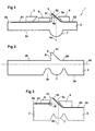
- Figure 1 shows a cross section through an inventive light-emitting semiconductor component 1.
- the semiconductor component has a carrier element 2 on its mounting side 2b an edge-emitting laser diode on a conductor layer 81 6 is mounted, for monitoring the operation of the laser diode 6 a diagonally cut monitor diode 3 or 4 (alternative), partly on a second section of the conductor layer 82 provided.
- the of the edge emitting laser diode 6 emitted light beams 6a are first on the coupling surface 51 of the reflector device 5 coupled into the material of the carrier element 2 and then on the reflection surface 52 of the reflector device - With the help of the increased reflectivity of the reflection layer 5a - in the optical axis of the spherical or aspherical lens trained light beam shaping device 7 forced.
- the emitted light 6a is from the reflector device 5 from its first to the mounting surface 2b parallel direction of propagation through the in for this purpose reflector surface 52 arranged at a 45 ° angle 6b reflects that they are at right angles to the exit side 2a of the carrier element 2 exits again.
- the 45 ° reflector surface 52 can be used as a carrier material for 100 wafers for example by an etching step with ethylenediamine Pyrocatechol (EDP) to be etched.
- EDP ethylenediamine Pyrocatechol
- the 45 ° reflector surface 52 can also be done by an etching step with reactive ion etching (RIE) can be created. To do this, a photoresist would have to be exposed for example by grayscale technology become.
- Vertical surfaces, such as the coupling surface 51 by means of so-called dry etching, for example again by means of reactive ion etching.
- the coupling-in surface 51 can also advantageously be provided with an antireflection layer be provided.
- FIG. 2 shows a carrier element 2 which has not yet been fitted, at which the spherical lens is not opposite to the exit side 2a of the support element 2 is designed so as to protrude by removing area 2c into the plane of the exit side 2a is worked into it.
- FIG 3 shows a further variant, again an edge emitting Laser diode 6 is used, this is in so-called “up-side-down assembly” attached, in which the light emitting edge on the lower mounting side of the active Semiconductor element 6 lies.
- the mounting surface 2b has a second lower level 2e because the beveled reflector surface 52 by the level of Assembly surface 2b emitted light bundle 6a still hit must become.
- a milling or sawing groove 2f is used here the simplified assembly of the laser diode 6 and the improved Decoupling the light at the edge of the laser diode 6.
- the reflection structure can be low and no other requirements compared to the thickness of the laser diode 6 must be made thus the emitted light beams 6a after their reflection in the optical axis of the light beam shaping device 7 lie.
- FIG. 21 A variant of the carrier element is shown in FIG this is composed of two sub-beams 21 and 22, those on their opposite smooth flat sides 21d and 22d are to be connected to one another.
- silicone fusion bonding technique or an adhesive technique are used.
- FIG. 5 shows a further variant of a carrier element 2 shown, using a curved reflective layer 55 comes, whereby the light beam shaping device 7 in the form of a lens becomes unnecessary.
- the shaping takes place in the example by the parabolic (elliptical) design the reflector device 5 or the reflection surface 55.
- Figure 6 shows an embodiment of a carrier element 2 with a beveled Coupling surface 51 and in the same way beveled reflection surface 52, both can Surfaces an angle 6b of 54.74 ° with respect to the horizontal exhibit.
- a 54.74 ° angle on one 111-level of the backing material can be used to manufacture the bevels the usual anisotropic etching technique can be used.
- the light beam emitted by the light source 6 6b in the direction of the light beam shaping device 7 a + 54.7 ° coupling surface 51 of the reflector device 5 in the optically transparent material of the carrier element 2 or the reflector device 5 is coupled and on the -54.7 ° reflection surface 52 of the reflector device 5 in the direction the lens 7 is reflected.
- the light beam 6a through the integrated lens surface of the spherical lens 7 focused. This light is guided by 45 ° deviating interfaces no longer in trivial 90 ° directions in the carrier material but in so-called off-axis directions.
- the guidance of the light path can by using the simple optical refraction and reflection laws be specified.
- Figure 7 is a light emitting semiconductor device shown in which only the light beam shaping device 7 formed by the formations of the carrier element 2 is.
- the reflector device is here by a Reflection surface 91 side surface of one of the components Encoder encapsulating body 3 and laser diode 6 encapsulating body 9 formed.
- the encapsulation body 9 can according to the invention as a chip made of a crystalline silicon substrate be made by the cavity with a known anisotropic etching process is produced, which for the reflective surface an angle of 54.7 ° in sufficient optical quality. In this case this is true Light no longer perpendicular to surface 2a and thus becomes according to the information given in FIG.
Landscapes
- Physics & Mathematics (AREA)
- General Physics & Mathematics (AREA)
- Optics & Photonics (AREA)
- Semiconductor Lasers (AREA)
Priority Applications (1)
| Application Number | Priority Date | Filing Date | Title |
|---|---|---|---|
| EP00108250A EP1146570A1 (fr) | 2000-04-14 | 2000-04-14 | Dispositif émetteur de lumière à semi-conducteur et methode pour la fabrication d'un support |
Applications Claiming Priority (1)
| Application Number | Priority Date | Filing Date | Title |
|---|---|---|---|
| EP00108250A EP1146570A1 (fr) | 2000-04-14 | 2000-04-14 | Dispositif émetteur de lumière à semi-conducteur et methode pour la fabrication d'un support |
Publications (1)
| Publication Number | Publication Date |
|---|---|
| EP1146570A1 true EP1146570A1 (fr) | 2001-10-17 |
Family
ID=8168481
Family Applications (1)
| Application Number | Title | Priority Date | Filing Date |
|---|---|---|---|
| EP00108250A Withdrawn EP1146570A1 (fr) | 2000-04-14 | 2000-04-14 | Dispositif émetteur de lumière à semi-conducteur et methode pour la fabrication d'un support |
Country Status (1)
| Country | Link |
|---|---|
| EP (1) | EP1146570A1 (fr) |
Cited By (7)
| Publication number | Priority date | Publication date | Assignee | Title |
|---|---|---|---|---|
| DE10209063C1 (de) * | 2002-02-22 | 2003-10-30 | Infineon Technologies Ag | Verfahren zur Herstellung einer monolithischen Laseranordnung |
| US6973110B2 (en) | 2002-02-22 | 2005-12-06 | Infineon Technologies Ag | Monolithic laser configuration |
| CN100391066C (zh) * | 2003-09-19 | 2008-05-28 | 安华高科技光纤Ip(新加坡)私人有限公司 | 集成光电子器件 |
| US7422929B2 (en) | 2003-09-19 | 2008-09-09 | Avago Technologies Fiber Ip Pte Ltd | Wafer-level packaging of optoelectronic devices |
| EP1981147A1 (fr) * | 2007-04-11 | 2008-10-15 | FELA Hitzinger GmbH | Unité d'illumination avec substrat transparent et diode électro-luminescente |
| DE112010004663B4 (de) | 2009-12-03 | 2019-01-17 | Autonetworks Technologies, Ltd. | Optisches Kommunikationsmodul |
| DE102020205189A1 (de) | 2020-04-23 | 2021-10-28 | Robert Bosch Gesellschaft mit beschränkter Haftung | Kappenvorrichtung, Kappenwafer und mikromechanische Verpackung |
Citations (8)
| Publication number | Priority date | Publication date | Assignee | Title |
|---|---|---|---|---|
| JPS57195209A (en) * | 1981-05-27 | 1982-11-30 | Toshiba Corp | Optical coupler |
| EP0117606A1 (fr) * | 1983-01-28 | 1984-09-05 | Xerox Corporation | Collecteur pour photodiodes groupées par rangées |
| US5577142A (en) * | 1994-11-17 | 1996-11-19 | Ant Nachrichtentechnik G.M.B.H. | Optical fiber transmitting and receiving communications device |
| DE19616969A1 (de) * | 1996-04-27 | 1997-10-30 | Bosch Gmbh Robert | Optische Baugruppe zur Ankopplung eines Lichtwellenleiters und Verfahren zur Herstellung derselben |
| US5761957A (en) * | 1996-02-08 | 1998-06-09 | Denso Corporation | Semiconductor pressure sensor that suppresses non-linear temperature characteristics |
| DE19718949A1 (de) * | 1997-05-05 | 1998-11-12 | Bosch Gmbh Robert | Elektrooptisches Modul |
| US5907151A (en) * | 1996-05-24 | 1999-05-25 | Siemens Aktiengesellschaft | Surface mountable optoelectronic transducer and method for its production |
| EP0992824A2 (fr) * | 1998-10-02 | 2000-04-12 | Siemens Aktiengesellschaft | Composant micro-optique et procédé de sa fabrication |
-
2000
- 2000-04-14 EP EP00108250A patent/EP1146570A1/fr not_active Withdrawn
Patent Citations (8)
| Publication number | Priority date | Publication date | Assignee | Title |
|---|---|---|---|---|
| JPS57195209A (en) * | 1981-05-27 | 1982-11-30 | Toshiba Corp | Optical coupler |
| EP0117606A1 (fr) * | 1983-01-28 | 1984-09-05 | Xerox Corporation | Collecteur pour photodiodes groupées par rangées |
| US5577142A (en) * | 1994-11-17 | 1996-11-19 | Ant Nachrichtentechnik G.M.B.H. | Optical fiber transmitting and receiving communications device |
| US5761957A (en) * | 1996-02-08 | 1998-06-09 | Denso Corporation | Semiconductor pressure sensor that suppresses non-linear temperature characteristics |
| DE19616969A1 (de) * | 1996-04-27 | 1997-10-30 | Bosch Gmbh Robert | Optische Baugruppe zur Ankopplung eines Lichtwellenleiters und Verfahren zur Herstellung derselben |
| US5907151A (en) * | 1996-05-24 | 1999-05-25 | Siemens Aktiengesellschaft | Surface mountable optoelectronic transducer and method for its production |
| DE19718949A1 (de) * | 1997-05-05 | 1998-11-12 | Bosch Gmbh Robert | Elektrooptisches Modul |
| EP0992824A2 (fr) * | 1998-10-02 | 2000-04-12 | Siemens Aktiengesellschaft | Composant micro-optique et procédé de sa fabrication |
Non-Patent Citations (1)
| Title |
|---|
| PATENT ABSTRACTS OF JAPAN vol. 007, no. 042 (P - 177) 19 February 1983 (1983-02-19) * |
Cited By (7)
| Publication number | Priority date | Publication date | Assignee | Title |
|---|---|---|---|---|
| DE10209063C1 (de) * | 2002-02-22 | 2003-10-30 | Infineon Technologies Ag | Verfahren zur Herstellung einer monolithischen Laseranordnung |
| US6973110B2 (en) | 2002-02-22 | 2005-12-06 | Infineon Technologies Ag | Monolithic laser configuration |
| CN100391066C (zh) * | 2003-09-19 | 2008-05-28 | 安华高科技光纤Ip(新加坡)私人有限公司 | 集成光电子器件 |
| US7422929B2 (en) | 2003-09-19 | 2008-09-09 | Avago Technologies Fiber Ip Pte Ltd | Wafer-level packaging of optoelectronic devices |
| EP1981147A1 (fr) * | 2007-04-11 | 2008-10-15 | FELA Hitzinger GmbH | Unité d'illumination avec substrat transparent et diode électro-luminescente |
| DE112010004663B4 (de) | 2009-12-03 | 2019-01-17 | Autonetworks Technologies, Ltd. | Optisches Kommunikationsmodul |
| DE102020205189A1 (de) | 2020-04-23 | 2021-10-28 | Robert Bosch Gesellschaft mit beschränkter Haftung | Kappenvorrichtung, Kappenwafer und mikromechanische Verpackung |
Similar Documents
| Publication | Publication Date | Title |
|---|---|---|
| EP0660467B1 (fr) | Elément optoélectronique et sa méthode de fabrication | |
| DE19601955C2 (de) | Optoelektronische Sendebaugruppe | |
| EP3535615B1 (fr) | Procédé de fabrication d'un système optique et système optique | |
| EP0631163B1 (fr) | Emetteur-récepteur optique bidirectionnel | |
| DE69815860T2 (de) | Integrierter strahlformer und seine verwendung | |
| DE60205806T2 (de) | Linse für Leuchtdioden | |
| DE69605265T2 (de) | Beleuchtungssystem mit integriertem Mikroteleskop in einer durchsichtigen Platte | |
| DE69935547T2 (de) | Mit Vertiefungen versehner, optischer Verteiler für Fahrzeug-Beleuchtungssystem | |
| DE69809922T2 (de) | Lichtlenkendes und lichtverteilendes, dünnes verwaltungssystem von einer oder mehreren lichtquellen und verfahren zur herstellung von optischen strukturen zur verwendung in einem solchen system | |
| EP2614694B1 (fr) | Procédé pour recouvrir un module puce-sur-plaque optoélectronique d'un revêtement | |
| DE69508511T2 (de) | Lichtleiter-Beleuchtungssystem zur Herstellung eines dünnen Beleuchtungselements | |
| EP2016449B1 (fr) | Un procédé de fabrication un composant optoélectronique | |
| EP0713113A1 (fr) | Dispositif optique émetteur et récepteur | |
| DE112004000955T5 (de) | Optischer Sender | |
| DE10250383B4 (de) | Leuchtdiodenanordnung mit Reflektor | |
| EP0735397A2 (fr) | Dispositif micro-optique pour transformer des faisceaux d'un arrangement de diodes laser et procédé de fabrication d'un tel dispositif | |
| DE19746025A1 (de) | Beleuchtungsanordnung für Fahrzeuge | |
| EP0397911A1 (fr) | Elément semi-conducteur opto-électronique | |
| WO2001004671A2 (fr) | Ensemble optoelectronique, composants pour cet ensemble et procede de fabrication dudit ensemble | |
| DE102017109083A1 (de) | Beleuchtungsvorrichtung und Verfahren zur Herstellung einer Beleuchtungsvorrichtung | |
| EP0833175A2 (fr) | Module opto-électronique pour la transmission optique bidirectionelle | |
| EP1805813B1 (fr) | Dispositif a semiconducteur emettant un rayonnement electromagnetique | |
| DE60133765T2 (de) | Strahlformer | |
| DE69305292T2 (de) | Beleuchtungseinrichtung | |
| DE69737474T2 (de) | Verfahren und system zur koppelung eines wellenleiters an eine komponente |
Legal Events
| Date | Code | Title | Description |
|---|---|---|---|
| PUAI | Public reference made under article 153(3) epc to a published international application that has entered the european phase |
Free format text: ORIGINAL CODE: 0009012 |
|
| AK | Designated contracting states |
Kind code of ref document: A1 Designated state(s): AT BE CH CY DE DK ES FI FR GB GR IE IT LI LU MC NL PT SE |
|
| AX | Request for extension of the european patent |
Free format text: AL;LT;LV;MK;RO;SI |
|
| AKX | Designation fees paid | ||
| REG | Reference to a national code |
Ref country code: DE Ref legal event code: 8566 |
|
| STAA | Information on the status of an ep patent application or granted ep patent |
Free format text: STATUS: THE APPLICATION IS DEEMED TO BE WITHDRAWN |
|
| 18D | Application deemed to be withdrawn |
Effective date: 20020418 |