EP1166443B1 - Dominologoik mit einer versorgungsspannung für einen vierphasentakt - Google Patents
Dominologoik mit einer versorgungsspannung für einen vierphasentakt Download PDFInfo
- Publication number
- EP1166443B1 EP1166443B1 EP00939594A EP00939594A EP1166443B1 EP 1166443 B1 EP1166443 B1 EP 1166443B1 EP 00939594 A EP00939594 A EP 00939594A EP 00939594 A EP00939594 A EP 00939594A EP 1166443 B1 EP1166443 B1 EP 1166443B1
- Authority
- EP
- European Patent Office
- Prior art keywords
- stage
- logic
- clock signal
- transistor
- output
- Prior art date
- Legal status (The legal status is an assumption and is not a legal conclusion. Google has not performed a legal analysis and makes no representation as to the accuracy of the status listed.)
- Expired - Lifetime
Links
Images

Classifications
-
- H—ELECTRICITY
- H03—ELECTRONIC CIRCUITRY
- H03K—PULSE TECHNIQUE
- H03K19/00—Logic circuits, i.e. having at least two inputs acting on one output; Inverting circuits
- H03K19/02—Logic circuits, i.e. having at least two inputs acting on one output; Inverting circuits using specified components
- H03K19/08—Logic circuits, i.e. having at least two inputs acting on one output; Inverting circuits using specified components using semiconductor devices
- H03K19/094—Logic circuits, i.e. having at least two inputs acting on one output; Inverting circuits using specified components using semiconductor devices using field-effect transistors
- H03K19/096—Synchronous circuits, i.e. using clock signals
- H03K19/0963—Synchronous circuits, i.e. using clock signals using transistors of complementary type
Definitions
- the present invention relates generally to digital electronic circuits, and more particularly relates to domino logic circuits.
- Modern integrated circuits are required to perform ever increasing tasks, and at ever increasing operating speeds.
- the requirement to increase operating speeds has often been met by increasing the clock speed at which a circuit operates. For example, while integrated circuit operation once occurred at clock speeds on the order of 10 to 50MHz, clock speeds now are often significantly greater than 100MHz, and in some cases are even on the order of 400MHz or more.
- circuit designers have also implemented circuitry which operates in a staged manner, with each stage evaluating over only a portion of a clock cycle and subsequent stages evaluating over subsequent portions of the clock cycle. That is, circuit designers arrange logic operations in a sequential manner, with each logic cell in the sequence providing information to subsequent logic cells in the sequence. These logic cells are evaluated during only a portion of the clock cycle, with subsequent logic cells evaluated in subsequent portions of the clock cycle. These logic cells therefore operate in a domino manner, and are often referred to as domino logic cells. The use of domino logic circuits allows designers to increase the effective speed of logic components without resorting to increasing clock speed.
- logic cells are often precharged. Precharging the logic cell is accomplished by driving the logic cell either to a mid range or to a high state. Driving the logic cell to a mid-range state allows the logic cell to change state with only a slight change in voltage. Thus the logic cell is able to change state at a faster rate than otherwise would occur. More often, however, the outputs of logic cells are driven to a high state. This is because PMOS transistors generally have a relatively large rise time due to parasitic capacitances. Accordingly, logic cell operation response time may be increased by charging the output to a high level prior to evaluation of the logic cell.
- a logic cell In a single clock cycle, therefore, a logic cell must be precharged, and thereafter allowed to evaluate its inputs. This is often accomplished by precharging the logic cell during one-half of a clock cycle, and allowing the logic cell to evaluate its inputs during the other half of the clock cycle.
- One constraint of such a methodology is that the logic cell must evaluate and provide its outputs to a subsequent logic cell in one half of the clock cycle. Further. subsequent precharging of the logic cell during the first half of a subsequent clock cycle may modify the outputs of the logic cell. Accordingly, the logic cell should not begin precharging until after the subsequent logic cell has evaluated its inputs.
- the derivation and use of additional signals based on the output of the logic cell should be kept to a minimum.
- One such additional signal is a complement of the output signal.
- Forming a complement of the output signal poses several problems.
- the additional inverter used to form the output signal complement places a delay in a signal path of an input to the subsequent logic stage, thereby limiting the period in which the logic cell has to evaluate its inputs. Further, this delay effects only the complementary signal path (ignoring fan out related delays), and the output signal path does not include this delay.
- a dual rail as opposed to signal rail, domino logic design is generally used.
- Single rail designs generally only have a single output per logic cell. Thus, a single rail design is monotonic in nature.
- a first set of logic cells produces a set of signals
- a second set, or rail, of logic cells produces the complements of these signals.
- Dual rail designs require significantly greater number of gates than a single rail design, resulting in increased chip layout space as well as increased power consumption.
- Fig. 22a discloses a system with a single domino rail logic circuit.
- the logic circuit has four stages, each stage including a logic cell coupled to a precharge circuit which comprises a single transistor.
- the present invention provides a logic circuit with a precharger comprising a logic cell and a precharge circuit coupled to the logic cell.
- the precharge circuit includes a first transistor and a second transistor, the first and second transistors having sources, drains and gates, with the drain of the first transistor coupled to the source of the second transistor, the drain of the second transistor coupled to the logic cell, the gate of the first transistor coupled to a first clock signal, the gate of the second transistor coupled to a second clock signal, and the second clock signal being approximately ninety degrees out of phase with the first clock signal.
- the ninety degree phase difference between the first and second clock signal allows for quarter clock cycle precharge time.
- the first clock signal and the second clock signal are of substantially the same frequency.
- the first transistor and the second transistor are both PMOS transistors.
- the logic cell has an output signal produced by a signal driver, and a complementary output signal produced by a first inverter coupled to the signal driver.
- the signal driver is preferably a second inverter and an input of the first inverter is coupled to an output of the second inverter.
- the logic cell is one of a plurality of logic cells in a sequence, and the logic cell provides the output and the complement of the output to a succeeding logic cell in the sequence
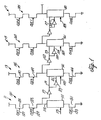
- FIG. 1 illustrates a single rail domino logic circuit of the present invention.
- the domino logic circuit has a first stage 11, a second stage 13, a third stage 15, and a fourth stage 17.
- the first stage provides a first stage output signal 19, and its complement 21, to the second stage.
- the second stage provides the third stage a second stage output signal 23, and its complement 25, to the third stage, and the third stage provides a third stage output signal 27, and its complement 29, to the fourth stage.
- the four stages are arranged in a domino fashion, with subsequent stages following preceding stages. Further, each stage provides a differential, i.e.. complementary. output signal to a subsequent stage.
- the domino logic circuit is provided four clock signals forming a four phase clocking scheme. This is accomplished by having each of the four clock signals be of the same frequency, but phase shifted with respect to the other clock signals in ninety degree increments. The clock signals, therefore, are symmetrically phase-shifted. Each stage receives two of these clock signals.
- the first stage includes NMOS first stage logic circuitry 111 which acts on logic inputs 113. Coupled to the first stage logic circuitry is precharge circuitry 121.
- the precharge circuity is a stacked PMOS pair, with a source of a first PMOS transistor 125 connected to a power supply and a source of a second PMOS transistor 123 connected to the drain on the first PMOS transistor. The drain of the second PMOS transistor is, in turn, connected to the logic circuitry.
- a gate of the first PMOS transistor of the precharge circuitry is provided a first clock signal (CLK1).
- a gate of the second PMOS transistor is provided a second clock signal (CLK2).
- the first and second clock signals are of the same frequency, but the second clock signal is phase shifted by 90° with respect to the first clock signal.
- the second clock signal has a rising edge delayed by a quarter clock cycle compared to the first clock signal.
- a falling edge of the second clock signal is delayed by a quarter clock cycle compared to a falling edge of the first clock signal. This is illustrated graphically in FIG. 2. As is illustrated in FIG. 2, at time t 2 the first clock signal has a rising edge, while the second clock signal remains low.
- the first and second clock signals are provided to the gate of the first PMOS transistor and the gate of the second PMOS transistor, respectively, the first and second PMOS transistors are both on only when both the first clock signal and the second clock signal are low.
- the precharge circuitry only precharges the NMOS logic for a quarter clock cycle.
- the drain of the second PMOS transistor is connected to an inverter 117.
- the inverter 117 provides the first stage output.
- One of the primary purposes of the inverter 117 is to drive the first stage output signal to the succeeding stage.
- the first stage output is provided to a second inverter 119.
- the second inverter provides the complement of the first stage output signal and similarly serves to drive the complement of the first stage output signal to the succeeding stage.
- the logic circuitry 111 is also connected to a drain of an NMOS driving transistor 131.
- the gate of the driving transistor 131 is provided the first clock signal.
- the driving transistor becomes active and the logic circuitry evaluates its inputs.
- the precharge circuitry becomes inactive when the first clock signal goes high, the output of the first stage is dependent on the inputs of the logic circuitry. Accordingly, for every complete clock cycle the first stage will precharge during a quarter of the clock cycle, and hold its output for three-quarters of the clock cycle at which time precharging once again occurs.
- the second stage is similar to the first stage.
- the second stage includes second stage logic circuitry 141.
- the second stage logic circuity receives logic inputs 143, as well as the complementary outputs from the first stage.
- the second stage also has precharge circuitry 145 comprising a stacked PMOS pair of transistors 147 and 149.
- the stacked PMOS pair of the second stage receives as inputs to their gates the second clock signal and a third clock signal (CLK3).
- CLK3 third clock signal
- the third clock signal is delayed by a quarter clock cycle with respect to the second clock signal, and is therefore 90° out of phase from the second clock signal and 180° out of phase from the first clock signal.
- the first stage precharges between times t 1 and t 2
- the second stage precharges between times t 2 and t 3 . Accordingly, the second stage operates with a quarter clock cycle delay as compared to the first stage.
- the drain of the second PMOS transistor 149 is connected to an inverter 153.
- the inverter 153 acts as a driving invertor, and produces the second stage output.
- the second stage output is also provided to an invertor 155 which provides the complement of the second stage output.
- the second stage output and the complement of the second stage output are provided to the third stage.
- the second stage logic circuitry 111 is also connected to a drain of an NMOS driving transistor 144.
- the gate of the driving transistor 144 is provided the second clock signal.
- the driving transistor becomes active and the logic circuitry evaluates its inputs.
- the precharge circuitry becomes inactive when the second clock signal goes high, the output of the first stage is dependent on the inputs of the logic circuitry. Accordingly. for every complete clock cycle the first stage will precharge during a quarter of the clock cycle and hold its output for three-quarters of the clock cycle at which time precharging once again occurs.
- the third stage is similar to the first and second stages. As with the first and second stages. the third stage includes logic circuitry 161 having as inputs the second stage output and the complement of the second stage output, as well as logic inputs 163. Coupled to the logic circuitry is precharge circuitry 165. As with the first and second stages, the precharge circuitry includes a stacked PMOS pair. The gates of the stacked PMOS pair are provided the third clock signal and a fourth clock signal (CLK4). The fourth clock signal is 90° out of phase from the third clock signal, and 270° out of phase from the first clock signal. Thus, the third stage logic circuitry is precharged beginning at time t 3 until time t 4 .
- the fourth stage is similar to the first, second, and third stages.
- the fourth stage includes logic circuitry 181 having as inputs the third stage output and the complement of the third stage output, as well as logic inputs 183. Coupled to the logic circuitry is precharge circuitry 185.
- the precharge circuitry includes a stacked PMOS pair. The gates of the stacked PMOS pair are provided a fourth clock signal and the first clock signal.
- the fourth stage logic circuitry is precharged beginning at a time t 4 until time t 5 , and evaluates beginning at time t 5 .
- FIG. 3 illustrates the timing diagram of the operation of the domino logic circuit of FIG. 1 when supplied the clock signals of FIG. 2.
- the second clock signal goes low, and the first clock signal is already low. Slightly after time t 1 , therefore, a signal S 115 at the drain of the second PMOS transistor 123 goes high.
- the change in the signal S 115 occurs approximately .2 nanoseconds after the second clock signal goes low.
- the first domino logic stage begins precharging.
- the output of the first stage S 19 stays low until the first clock signal goes high at time t 2 . Once the first clock signal goes high at time t 2 the first domino logic stage evaluates and the output signal S 19 may change depending on the results of that evaluation.
- the second domino logic stage begins precharging also at time t 2 as the second clock signal is low and the third clock signal goes low.
- the second domino logic stage continues precharging until time t 3 when the second clock signal goes high and the second domino logic stage evaluates. Accordingly, the first domino logic stage should have a completed evaluation and propagated its output signals to the second domino logic stage.
- the third domino logic stage begins precharging At time t 3 as the fourth clock signals goes low arid the third clock signal is already low. Thus. shortly after time t 3 the output from the inverter, signal S 27 , goes low.
- the third clock signal goes high at time t 4 and the third domino logic stage begins evaluation. Accordingly, by time t 4 the second domino logic stage should have evaluated its inputs and propagated its outputs to the third domino stage. Also at time t 4 the fourth domino logic stage begins precharging as the first clock signal goes low and a fourth clock signal is already low.
- the second clock signal goes low and the first signal is already low. Accordingly, the first domino logic stage once again begins precharging. Shortly after time t 5 therefore the first stage output goes low. As the first stage output going low may affect the second stage output, the third stage should have completed evaluation prior to the time at which the first stage begins precharging, taking into account signal propagation delays.
- each stage of the four stage single rail domino logic circuit precharges for one-quarter of a clock cycle, and evaluates and holds its output for each remaining three-quarters of a clock cycle. This is illustrated in Table I.
- the first stage precharges during a first quarter clock period, and evaluates during a second quarter clock period.
- the first stage holds its outputs during a third quarter clock period, during which time a second stage evaluates, and further holds its outputs during a fourth quarter clock cycle while the third stage evaluates. Holding the outputs for two quarter clock periods aids in preventing a race condition.
- T t p + t e , where t p is the time allotted for precharging and t e is the time allotted for evaluation of inputs and holding outputs stable so that subsequent stages may evaluate.
- t p should be greater than or equal to the actual precharge time t precharge, plus any time required to account for clock skew.
- t e should be greater than or equal to the actual evaluation time plus the hold time plus any time required to account for signal skew.
- t p is a quarter clock cycle
- evaluation of inputs is a greater clock cycle
- hold time is budgeted as two quarter clock cycles (although it should be noted that the logic for a stage is isolated from both V DD and V SS for only a quarter clock cycle).
- T t precharge + 1 ⁇ 4T + t hold + 2t skew
- T t precharge + 3 ⁇ 4T + 2t skew .
- the present invention therefore provides a single rail domino logic circuit for a four-phase clocking scheme.
- the signal rail domino logic circuit of the present invention is able to provide complementary output signals without the need of a dual rail design.
- a 64 bit adder using the single rail domino logic circuit of the present invention, under .25 micron technology and provided a 250 MHZ clock frequency results in reduced gate count of approximately thirty percent. Accordingly, the present invention provides reduced gate count with respect to a dual rail design.
Landscapes
- Engineering & Computer Science (AREA)
- Power Engineering (AREA)
- Physics & Mathematics (AREA)
- Computer Hardware Design (AREA)
- Computing Systems (AREA)
- General Engineering & Computer Science (AREA)
- Mathematical Physics (AREA)
- Logic Circuits (AREA)
Claims (6)
- Logikschaltung (11, 13, 15, 17) mit einem Vorlader, umfassend:dadurch gekennzeichnet, daß die Vorladeschaltung weiterhin einen zweiten Transistor (123, 149) mit einem Source, einem Drain und einem Gate enthält, wobei der Drain des ersten Transistors (125, 147) an das Source des zweiten Transistors (123, 149) angekoppelt ist, der Drain des zweiten Transistors (123, 149) an die Logikzelle (111, 141, 161, 181), das Gate des zweiten Transistors (123, 149) an ein zweites Taktsignal (CLK2, CLK3, CLK4, CLK1) angekoppelt ist und das zweite Taktsignal (CLK2, CLK3, CLK4, CLK1) zum ersten Taktsignal (CLK1, CLK2, CLK3, CLK4) um etwa 90 Grad außer Phase ist.eine Logikzelle (111, 141, 161, 181);eine Vorladeschaltung (121, 145, 165, 185), die an die Logikschaltung angekoppelt ist, mit einem ersten Transistor (125, 147), der ein Source, einen Drain und ein Gate aufweist, wobei das Gate des ersten Transistors (125, 147) an ein erstes Taktsignal (CLK1, CLK2, CLK3, CLK4) angekoppelt ist,
- Logikschaltung mit einem Vorlader nach Anspruch 1, wobei das erste Taktsignal (CLK1, CLK2, CLK3, CLK4) und das zweite Taktsignal (CLK2, CLK3, CLK4, CLK1) im wesentlichen die gleiche Frequenz aufweisen.
- Logikschaltung mit einem Vorlader nach Anspruch 1, wobei sowohl der erste Transistor (125, 147) als auch der zweite Transistor (123, 149) ein PMOS-Transistor ist.
- Logikschaltung mit einem Vorlader nach einem der Ansprüche 1 bis 3, wobei die Logikzelle (111, 141, 161, 181) ein von einem Signaltreiber (117, 153) erzeugtes Ausgangssignal (19, 23, 27) und ein komplementäres Ausgangssignal (21, 125, 29), das von einem an den Signaltreiber (117, 153) angekoppelten ersten Inverter (119, 155) erzeugt wird, aufweist.
- Logikschaltung mit einem Vorlader nach Anspruch 4, wobei der Signaltreiber ein zweiter Inverter (117, 153) ist und ein Eingang des ersten Inverters (119, 155) an einen Ausgang des zweiten Inverters (117, 153) angekoppelt ist.
- Logikschaltung mit einem Vorlader nach einem der Ansprüche 1 bis 5, wobei die Logikzelle eine von mehreren Logikzellen (111, 141, 161, 181) in einer Folge ist und die Logikzelle (111, 141, 161) den Ausgang (19, 23, 27) und das Komplement (21, 125, 29) des Ausgangs an eine Logikzelle (141, 161, 181) in der Folge führt.
Applications Claiming Priority (3)
| Application Number | Priority Date | Filing Date | Title |
|---|---|---|---|
| US09/326,161 US6265899B1 (en) | 1999-06-04 | 1999-06-04 | Single rail domino logic for four-phase clocking scheme |
| US326161 | 1999-06-04 | ||
| PCT/US2000/015533 WO2000076068A2 (en) | 1999-06-04 | 2000-06-05 | Single rail domino logic for four-phase clocking scheme |
Publications (3)
| Publication Number | Publication Date |
|---|---|
| EP1166443A2 EP1166443A2 (de) | 2002-01-02 |
| EP1166443A4 EP1166443A4 (de) | 2002-01-02 |
| EP1166443B1 true EP1166443B1 (de) | 2003-05-02 |
Family
ID=23271058
Family Applications (1)
| Application Number | Title | Priority Date | Filing Date |
|---|---|---|---|
| EP00939594A Expired - Lifetime EP1166443B1 (de) | 1999-06-04 | 2000-06-05 | Dominologoik mit einer versorgungsspannung für einen vierphasentakt |
Country Status (6)
| Country | Link |
|---|---|
| US (1) | US6265899B1 (de) |
| EP (1) | EP1166443B1 (de) |
| JP (1) | JP2003501935A (de) |
| CA (1) | CA2338114C (de) |
| DE (1) | DE60002453D1 (de) |
| WO (1) | WO2000076068A2 (de) |
Families Citing this family (24)
| Publication number | Priority date | Publication date | Assignee | Title |
|---|---|---|---|---|
| US20040019923A1 (en) * | 1997-10-16 | 2004-01-29 | Ivarie Robert D. | Exogenous proteins expressed in avians and their eggs |
| US6441648B1 (en) * | 2001-05-09 | 2002-08-27 | Intel Corporation | Double data rate dynamic logic |
| US7417465B2 (en) * | 2002-08-14 | 2008-08-26 | Via Technologies, Inc. | N-domino output latch |
| US7187209B2 (en) * | 2003-08-13 | 2007-03-06 | Via Technologies, Inc. | Non-inverting domino register |
| US7187211B2 (en) * | 2002-08-14 | 2007-03-06 | Via Technologies, Inc. | P-domino output latch |
| US7193445B2 (en) * | 2002-08-14 | 2007-03-20 | Ip-First, Llc | Non-inverting domino register |
| US7123056B2 (en) * | 2002-12-09 | 2006-10-17 | Mosaid Technologies Incorporated | Clock logic domino circuits for high-speed and energy efficient microprocessor pipelines |
| US7095400B2 (en) * | 2003-07-28 | 2006-08-22 | Inventec Appliances Corp. | Method of automatically enabling or disabling backlight of electronic device based on a predetermined time |
| TWI237265B (en) * | 2003-08-13 | 2005-08-01 | Ip First Llc | Non-inverting domino register |
| US7187210B2 (en) * | 2003-08-13 | 2007-03-06 | Via Technologies, Inc. | P-domino register |
| TWI281319B (en) * | 2004-12-27 | 2007-05-11 | Via Tech Inc | Non-inverting domino register |
| US9679602B2 (en) | 2006-06-14 | 2017-06-13 | Seagate Technology Llc | Disc drive circuitry swap |
| US7317339B1 (en) * | 2006-06-16 | 2008-01-08 | Via Technologies, Inc. | N-domino register with accelerated non-discharge path |
| US7321243B1 (en) * | 2006-06-16 | 2008-01-22 | Via Technologies, Inc. | P-domino register with accelerated non-charge path |
| US7348806B2 (en) | 2006-08-11 | 2008-03-25 | Via Technologies, Inc. | Accelerated N-channel dynamic register |
| US7382161B2 (en) * | 2006-08-11 | 2008-06-03 | Via Technologies, Inc. | Accelerated P-channel dynamic register |
| US9305590B2 (en) | 2007-10-16 | 2016-04-05 | Seagate Technology Llc | Prevent data storage device circuitry swap |
| US7990180B2 (en) * | 2009-09-09 | 2011-08-02 | Via Technologies, Inc. | Fast dynamic register |
| KR101911060B1 (ko) | 2012-03-19 | 2018-10-23 | 삼성전자주식회사 | 푸터가 없는 np 도미노 로직 회로와 이를 포함하는 장치들 |
| KR101908409B1 (ko) * | 2012-04-02 | 2018-10-17 | 삼성전자 주식회사 | 클럭 지연 도미노 로직 회로 및 이를 포함하는 장치들 |
| US8860463B1 (en) | 2013-04-24 | 2014-10-14 | Via Technologies, Inc. | Fast dynamic register with transparent latch |
| US9742408B1 (en) * | 2016-09-23 | 2017-08-22 | International Business Machines Corporation | Dynamic decode circuit with active glitch control |
| US10374604B1 (en) | 2018-08-12 | 2019-08-06 | International Business Machines Corporation | Dynamic decode circuit low power application |
| KR102557751B1 (ko) * | 2020-07-15 | 2023-07-24 | 한양대학교 산학협력단 | 단일 극성 다이나믹 로직 회로 |
Family Cites Families (27)
| Publication number | Priority date | Publication date | Assignee | Title |
|---|---|---|---|---|
| US4700086A (en) | 1985-04-23 | 1987-10-13 | International Business Machines Corporation | Consistent precharge circuit for cascode voltage switch logic |
| FR2596595B1 (fr) | 1986-03-28 | 1988-05-13 | Radiotechnique Compelec | Porte logique mos du type domino |
| US5015882A (en) | 1986-09-03 | 1991-05-14 | Texas Instruments Incorporated | Compound domino CMOS circuit |
| US5208489A (en) | 1986-09-03 | 1993-05-04 | Texas Instruments Incorporated | Multiple compound domino logic circuit |
| US4985643A (en) | 1988-06-24 | 1991-01-15 | National Semiconductor Corporation | Speed enhancement technique for CMOS circuits |
| US4896057A (en) | 1988-09-14 | 1990-01-23 | United States Of America As Represented By The Administrator, National Aeronautics And Space Administration | High-speed dynamic domino circuit implemented with gaas mesfets |
| US5041742A (en) | 1990-05-09 | 1991-08-20 | Motorola, Inc. | Structured scan path circuit for incorporating domino logic |
| US5121003A (en) | 1990-10-10 | 1992-06-09 | Hal Computer Systems, Inc. | Zero overhead self-timed iterative logic |
| US5208490A (en) | 1991-04-12 | 1993-05-04 | Hewlett-Packard Company | Functionally complete family of self-timed dynamic logic circuits |
| US5263173A (en) * | 1991-07-10 | 1993-11-16 | Hewlett-Packard Company | High speed clocked output driver for switching logic levels of an output pad at integer and integer and a half clock cycles |
| US5146115A (en) | 1991-07-26 | 1992-09-08 | Zilog, Inc. | Domino-logic decoder |
| US5369651A (en) | 1992-06-30 | 1994-11-29 | Intel Corporation | Multiplexed byte enable bus for partial word writes to ECC protected memory |
| US5402012A (en) | 1993-04-19 | 1995-03-28 | Vlsi Technology, Inc. | Sequentially clocked domino-logic cells |
| US5453708A (en) | 1995-01-04 | 1995-09-26 | Intel Corporation | Clocking scheme for latching of a domino output |
| US5541536A (en) | 1995-03-01 | 1996-07-30 | Sun Microsystems, Inc. | Rubberband logic |
| US5517136A (en) | 1995-03-03 | 1996-05-14 | Intel Corporation | Opportunistic time-borrowing domino logic |
| US5661675A (en) | 1995-03-31 | 1997-08-26 | Intel Corporation | Positive feedback circuit for fast domino logic |
| US5642061A (en) | 1995-04-17 | 1997-06-24 | Hitachi America, Ltd. | Short circuit current free dynamic logic clock timing |
| US5550490A (en) | 1995-05-25 | 1996-08-27 | International Business Machines Corporation | Single-rail self-resetting logic circuitry |
| US5565798A (en) | 1995-08-21 | 1996-10-15 | International Business Machines Corporation | Self-timed control circuit for self-resetting logic circuitry |
| US5712578A (en) | 1995-12-27 | 1998-01-27 | Intel Corporation | PLA architecture having improved clock signal to output timing using a type-I domino and plane |
| US5825208A (en) * | 1996-05-20 | 1998-10-20 | International Business Machines Corporation | Method and apparatus for fast evaluation of dynamic CMOS logic circuits |
| US5821778A (en) * | 1996-07-19 | 1998-10-13 | Texas Instruments Incorporated | Using cascode transistors having low threshold voltages |
| US5796282A (en) | 1996-08-12 | 1998-08-18 | Intel Corporation | Latching mechanism for pulsed domino logic with inherent race margin and time borrowing |
| AU5800698A (en) | 1996-12-27 | 1998-07-31 | Intel Corporation | Single-phase domino time borrowing logic with clocks at first and last stages and latch at last stage |
| US6040716A (en) * | 1997-05-19 | 2000-03-21 | Texas Instruments Incorporated | Domino logic circuits, systems, and methods with precharge control based on completion of evaluation by the subsequent domino logic stage |
| TW344131B (en) * | 1997-06-03 | 1998-11-01 | Nat Science Council | A 1.5V bootstrapped all-N-logic true-single-phase CMOS dynamic logic circuit suitable for low supply voltage and high speed pipelined |
-
1999
- 1999-06-04 US US09/326,161 patent/US6265899B1/en not_active Expired - Lifetime
-
2000
- 2000-06-05 JP JP2001502234A patent/JP2003501935A/ja active Pending
- 2000-06-05 CA CA002338114A patent/CA2338114C/en not_active Expired - Fee Related
- 2000-06-05 DE DE60002453T patent/DE60002453D1/de not_active Expired - Lifetime
- 2000-06-05 EP EP00939594A patent/EP1166443B1/de not_active Expired - Lifetime
- 2000-06-05 WO PCT/US2000/015533 patent/WO2000076068A2/en not_active Ceased
Also Published As
| Publication number | Publication date |
|---|---|
| EP1166443A2 (de) | 2002-01-02 |
| US6265899B1 (en) | 2001-07-24 |
| DE60002453D1 (de) | 2003-06-05 |
| EP1166443A4 (de) | 2002-01-02 |
| WO2000076068A3 (en) | 2001-10-11 |
| CA2338114A1 (en) | 2000-12-14 |
| CA2338114C (en) | 2003-04-15 |
| WO2000076068A2 (en) | 2000-12-14 |
| JP2003501935A (ja) | 2003-01-14 |
Similar Documents
| Publication | Publication Date | Title |
|---|---|---|
| EP1166443B1 (de) | Dominologoik mit einer versorgungsspannung für einen vierphasentakt | |
| US5880608A (en) | Pulsed domino latches | |
| US5517136A (en) | Opportunistic time-borrowing domino logic | |
| US7034578B2 (en) | N-domino output latch with accelerated evaluate path | |
| US5841300A (en) | Semiconductor integrated circuit apparatus | |
| US7064584B2 (en) | P-domino output latch with accelerated evaluate path | |
| US7317339B1 (en) | N-domino register with accelerated non-discharge path | |
| US4692637A (en) | CMOS logic circuit with single clock pulse | |
| US5821775A (en) | Method and apparatus to interface monotonic and non-monotonic domino logic | |
| US6331793B1 (en) | Apparatus, method and system for pulse passgate topologies | |
| US20040036510A1 (en) | Clock signal propagation gate and semiconductor integrated circuit including same | |
| US6323698B1 (en) | Apparatus, method and system for providing LVS enables together with LVS data | |
| US7528630B2 (en) | High speed flip-flop | |
| EP1868292B1 (de) | Schnelle P-Domino-Registerschaltung | |
| US7193445B2 (en) | Non-inverting domino register | |
| US20040113658A1 (en) | Dynamic logic register | |
| US20050055538A1 (en) | Dynamic logic return-to-zero latching mechanism | |
| CN102318190A (zh) | 基于前馈的脉宽缩减延迟线 | |
| US6958629B2 (en) | Single stage, level restore circuit with mixed signal inputs | |
| US6794903B2 (en) | CMOS parallel dynamic logic and speed enhanced static logic | |
| US6404253B1 (en) | High speed, low setup time voltage sensing flip-flop | |
| US6239622B1 (en) | Self-timed domino circuit | |
| JP3754028B2 (ja) | 半導体装置 | |
| JP3319615B2 (ja) | Pla | |
| US7245149B2 (en) | Dynamic programmable logic array having enable unit |
Legal Events
| Date | Code | Title | Description |
|---|---|---|---|
| PUAI | Public reference made under article 153(3) epc to a published international application that has entered the european phase |
Free format text: ORIGINAL CODE: 0009012 |
|
| 17P | Request for examination filed |
Effective date: 20010305 |
|
| A4 | Supplementary search report drawn up and despatched |
Effective date: 20010828 |
|
| AK | Designated contracting states |
Kind code of ref document: A4 Designated state(s): AT BE CH CY DE DK ES FI FR GB GR IE IT LI LU MC NL PT SE Kind code of ref document: A2 Designated state(s): AT BE CH CY DE DK ES FI FR GB GR IE IT LI LU MC NL PT SE |
|
| AX | Request for extension of the european patent |
Free format text: AL;LT;LV;MK;RO;SI |
|
| 17Q | First examination report despatched |
Effective date: 20020510 |
|
| GRAH | Despatch of communication of intention to grant a patent |
Free format text: ORIGINAL CODE: EPIDOS IGRA |
|
| GRAH | Despatch of communication of intention to grant a patent |
Free format text: ORIGINAL CODE: EPIDOS IGRA |
|
| GRAA | (expected) grant |
Free format text: ORIGINAL CODE: 0009210 |
|
| AK | Designated contracting states |
Designated state(s): DE GB |
|
| REG | Reference to a national code |
Ref country code: GB Ref legal event code: FG4D |
|
| REF | Corresponds to: |
Ref document number: 60002453 Country of ref document: DE Date of ref document: 20030605 Kind code of ref document: P |
|
| REG | Reference to a national code |
Ref country code: IE Ref legal event code: FG4D |
|
| PG25 | Lapsed in a contracting state [announced via postgrant information from national office to epo] |
Ref country code: DE Free format text: LAPSE BECAUSE OF FAILURE TO SUBMIT A TRANSLATION OF THE DESCRIPTION OR TO PAY THE FEE WITHIN THE PRESCRIBED TIME-LIMIT Effective date: 20030805 |
|
| LTIE | Lt: invalidation of european patent or patent extension |
Effective date: 20030502 |
|
| PLBE | No opposition filed within time limit |
Free format text: ORIGINAL CODE: 0009261 |
|
| STAA | Information on the status of an ep patent application or granted ep patent |
Free format text: STATUS: NO OPPOSITION FILED WITHIN TIME LIMIT |
|
| REG | Reference to a national code |
Ref country code: IE Ref legal event code: MM4A |
|
| 26N | No opposition filed |
Effective date: 20040203 |
|
| PG25 | Lapsed in a contracting state [announced via postgrant information from national office to epo] |
Ref country code: GB Free format text: LAPSE BECAUSE OF NON-PAYMENT OF DUE FEES Effective date: 20040605 |
|
| GBPC | Gb: european patent ceased through non-payment of renewal fee |
Effective date: 20040605 |