EP1169623B1 - Obturateur optique pour instrument de spectroscopie - Google Patents
Obturateur optique pour instrument de spectroscopie Download PDFInfo
- Publication number
- EP1169623B1 EP1169623B1 EP01905489.9A EP01905489A EP1169623B1 EP 1169623 B1 EP1169623 B1 EP 1169623B1 EP 01905489 A EP01905489 A EP 01905489A EP 1169623 B1 EP1169623 B1 EP 1169623B1
- Authority
- EP
- European Patent Office
- Prior art keywords
- light
- shutter
- detector
- spectroscopy apparatus
- bimorph
- Prior art date
- Legal status (The legal status is an assumption and is not a legal conclusion. Google has not performed a legal analysis and makes no representation as to the accuracy of the status listed.)
- Expired - Lifetime
Links
- 230000003287 optical effect Effects 0.000 title claims abstract description 39
- 238000004611 spectroscopical analysis Methods 0.000 title claims abstract description 27
- 230000003595 spectral effect Effects 0.000 claims abstract description 37
- 238000005259 measurement Methods 0.000 claims abstract description 24
- 238000004458 analytical method Methods 0.000 claims abstract description 9
- 239000007787 solid Substances 0.000 claims abstract description 6
- 230000001681 protective effect Effects 0.000 claims abstract 4
- 230000033001 locomotion Effects 0.000 claims description 28
- 238000012546 transfer Methods 0.000 claims description 9
- 239000000463 material Substances 0.000 claims description 8
- 239000000758 substrate Substances 0.000 claims description 6
- 230000001052 transient effect Effects 0.000 claims description 3
- 239000002131 composite material Substances 0.000 claims description 2
- 239000000835 fiber Substances 0.000 claims description 2
- 238000002347 injection Methods 0.000 claims description 2
- 239000007924 injection Substances 0.000 claims description 2
- 238000012806 monitoring device Methods 0.000 claims 1
- 238000012544 monitoring process Methods 0.000 claims 1
- 230000000903 blocking effect Effects 0.000 abstract description 6
- 230000005284 excitation Effects 0.000 abstract description 6
- 239000000523 sample Substances 0.000 description 19
- 238000010521 absorption reaction Methods 0.000 description 12
- 230000010354 integration Effects 0.000 description 10
- 238000000034 method Methods 0.000 description 10
- 238000013459 approach Methods 0.000 description 7
- 238000006073 displacement reaction Methods 0.000 description 7
- 230000008901 benefit Effects 0.000 description 6
- 238000010586 diagram Methods 0.000 description 6
- 230000000694 effects Effects 0.000 description 6
- 230000008569 process Effects 0.000 description 6
- 239000000126 substance Substances 0.000 description 6
- 238000001636 atomic emission spectroscopy Methods 0.000 description 4
- 239000013626 chemical specie Substances 0.000 description 4
- 238000000921 elemental analysis Methods 0.000 description 4
- 230000010355 oscillation Effects 0.000 description 4
- 229910052729 chemical element Inorganic materials 0.000 description 3
- 239000002184 metal Substances 0.000 description 3
- 229910052751 metal Inorganic materials 0.000 description 3
- 238000004847 absorption spectroscopy Methods 0.000 description 2
- 238000007792 addition Methods 0.000 description 2
- 239000000538 analytical sample Substances 0.000 description 2
- 238000003321 atomic absorption spectrophotometry Methods 0.000 description 2
- 239000003990 capacitor Substances 0.000 description 2
- 230000001419 dependent effect Effects 0.000 description 2
- 238000004993 emission spectroscopy Methods 0.000 description 2
- 239000011888 foil Substances 0.000 description 2
- 238000009616 inductively coupled plasma Methods 0.000 description 2
- 230000007246 mechanism Effects 0.000 description 2
- 239000000203 mixture Substances 0.000 description 2
- 238000012986 modification Methods 0.000 description 2
- 230000004048 modification Effects 0.000 description 2
- 230000036961 partial effect Effects 0.000 description 2
- 238000009416 shuttering Methods 0.000 description 2
- 238000002798 spectrophotometry method Methods 0.000 description 2
- 238000000870 ultraviolet spectroscopy Methods 0.000 description 2
- 206010010099 Combined immunodeficiency Diseases 0.000 description 1
- RYGMFSIKBFXOCR-UHFFFAOYSA-N Copper Chemical compound [Cu] RYGMFSIKBFXOCR-UHFFFAOYSA-N 0.000 description 1
- 206010034960 Photophobia Diseases 0.000 description 1
- 241000287219 Serinus canaria Species 0.000 description 1
- 230000009471 action Effects 0.000 description 1
- 239000000853 adhesive Substances 0.000 description 1
- 230000001070 adhesive effect Effects 0.000 description 1
- 238000005452 bending Methods 0.000 description 1
- 230000005540 biological transmission Effects 0.000 description 1
- 238000001444 catalytic combustion detection Methods 0.000 description 1
- 238000009614 chemical analysis method Methods 0.000 description 1
- 238000001360 collision-induced dissociation Methods 0.000 description 1
- 239000000470 constituent Substances 0.000 description 1
- 238000010276 construction Methods 0.000 description 1
- 229910052802 copper Inorganic materials 0.000 description 1
- 239000010949 copper Substances 0.000 description 1
- 238000013016 damping Methods 0.000 description 1
- 238000001514 detection method Methods 0.000 description 1
- 239000006185 dispersion Substances 0.000 description 1
- 229920006333 epoxy cement Polymers 0.000 description 1
- 230000007717 exclusion Effects 0.000 description 1
- 239000011152 fibreglass Substances 0.000 description 1
- 238000001914 filtration Methods 0.000 description 1
- 239000003574 free electron Substances 0.000 description 1
- 239000011521 glass Substances 0.000 description 1
- 150000002500 ions Chemical class 0.000 description 1
- HFGPZNIAWCZYJU-UHFFFAOYSA-N lead zirconate titanate Chemical compound [O-2].[O-2].[O-2].[O-2].[O-2].[Ti+4].[Zr+4].[Pb+2] HFGPZNIAWCZYJU-UHFFFAOYSA-N 0.000 description 1
- 229910052451 lead zirconate titanate Inorganic materials 0.000 description 1
- 230000031700 light absorption Effects 0.000 description 1
- 208000013469 light sensitivity Diseases 0.000 description 1
- 230000000670 limiting effect Effects 0.000 description 1
- 230000005855 radiation Effects 0.000 description 1
- 230000009467 reduction Effects 0.000 description 1
- 230000002829 reductive effect Effects 0.000 description 1
- 230000004044 response Effects 0.000 description 1
- 230000002441 reversible effect Effects 0.000 description 1
- 229920006395 saturated elastomer Polymers 0.000 description 1
- 238000012306 spectroscopic technique Methods 0.000 description 1
- 238000001228 spectrum Methods 0.000 description 1
- 230000003068 static effect Effects 0.000 description 1
- 230000001960 triggered effect Effects 0.000 description 1
Images


Classifications
-
- G—PHYSICS
- G01—MEASURING; TESTING
- G01J—MEASUREMENT OF INTENSITY, VELOCITY, SPECTRAL CONTENT, POLARISATION, PHASE OR PULSE CHARACTERISTICS OF INFRARED, VISIBLE OR ULTRAVIOLET LIGHT; COLORIMETRY; RADIATION PYROMETRY
- G01J3/00—Spectrometry; Spectrophotometry; Monochromators; Measuring colours
- G01J3/02—Details
-
- G—PHYSICS
- G01—MEASURING; TESTING
- G01J—MEASUREMENT OF INTENSITY, VELOCITY, SPECTRAL CONTENT, POLARISATION, PHASE OR PULSE CHARACTERISTICS OF INFRARED, VISIBLE OR ULTRAVIOLET LIGHT; COLORIMETRY; RADIATION PYROMETRY
- G01J5/00—Radiation pyrometry, e.g. infrared or optical thermometry
- G01J5/02—Constructional details
- G01J5/08—Optical arrangements
- G01J5/0803—Arrangements for time-dependent attenuation of radiation signals
- G01J5/0805—Means for chopping radiation
-
- G—PHYSICS
- G01—MEASURING; TESTING
- G01J—MEASUREMENT OF INTENSITY, VELOCITY, SPECTRAL CONTENT, POLARISATION, PHASE OR PULSE CHARACTERISTICS OF INFRARED, VISIBLE OR ULTRAVIOLET LIGHT; COLORIMETRY; RADIATION PYROMETRY
- G01J3/00—Spectrometry; Spectrophotometry; Monochromators; Measuring colours
- G01J3/02—Details
- G01J3/0205—Optical elements not provided otherwise, e.g. optical manifolds, diffusers, windows
- G01J3/0213—Optical elements not provided otherwise, e.g. optical manifolds, diffusers, windows using attenuators
-
- G—PHYSICS
- G01—MEASURING; TESTING
- G01J—MEASUREMENT OF INTENSITY, VELOCITY, SPECTRAL CONTENT, POLARISATION, PHASE OR PULSE CHARACTERISTICS OF INFRARED, VISIBLE OR ULTRAVIOLET LIGHT; COLORIMETRY; RADIATION PYROMETRY
- G01J3/00—Spectrometry; Spectrophotometry; Monochromators; Measuring colours
- G01J3/02—Details
- G01J3/0205—Optical elements not provided otherwise, e.g. optical manifolds, diffusers, windows
- G01J3/0227—Optical elements not provided otherwise, e.g. optical manifolds, diffusers, windows using notch filters
-
- G—PHYSICS
- G01—MEASURING; TESTING
- G01J—MEASUREMENT OF INTENSITY, VELOCITY, SPECTRAL CONTENT, POLARISATION, PHASE OR PULSE CHARACTERISTICS OF INFRARED, VISIBLE OR ULTRAVIOLET LIGHT; COLORIMETRY; RADIATION PYROMETRY
- G01J3/00—Spectrometry; Spectrophotometry; Monochromators; Measuring colours
- G01J3/02—Details
- G01J3/0205—Optical elements not provided otherwise, e.g. optical manifolds, diffusers, windows
- G01J3/0229—Optical elements not provided otherwise, e.g. optical manifolds, diffusers, windows using masks, aperture plates, spatial light modulators or spatial filters, e.g. reflective filters
-
- G—PHYSICS
- G01—MEASURING; TESTING
- G01J—MEASUREMENT OF INTENSITY, VELOCITY, SPECTRAL CONTENT, POLARISATION, PHASE OR PULSE CHARACTERISTICS OF INFRARED, VISIBLE OR ULTRAVIOLET LIGHT; COLORIMETRY; RADIATION PYROMETRY
- G01J3/00—Spectrometry; Spectrophotometry; Monochromators; Measuring colours
- G01J3/02—Details
- G01J3/0205—Optical elements not provided otherwise, e.g. optical manifolds, diffusers, windows
- G01J3/0232—Optical elements not provided otherwise, e.g. optical manifolds, diffusers, windows using shutters
-
- G—PHYSICS
- G01—MEASURING; TESTING
- G01J—MEASUREMENT OF INTENSITY, VELOCITY, SPECTRAL CONTENT, POLARISATION, PHASE OR PULSE CHARACTERISTICS OF INFRARED, VISIBLE OR ULTRAVIOLET LIGHT; COLORIMETRY; RADIATION PYROMETRY
- G01J3/00—Spectrometry; Spectrophotometry; Monochromators; Measuring colours
- G01J3/12—Generating the spectrum; Monochromators
- G01J3/18—Generating the spectrum; Monochromators using diffraction elements, e.g. grating
- G01J3/1809—Echelle gratings
-
- G—PHYSICS
- G01—MEASURING; TESTING
- G01J—MEASUREMENT OF INTENSITY, VELOCITY, SPECTRAL CONTENT, POLARISATION, PHASE OR PULSE CHARACTERISTICS OF INFRARED, VISIBLE OR ULTRAVIOLET LIGHT; COLORIMETRY; RADIATION PYROMETRY
- G01J3/00—Spectrometry; Spectrophotometry; Monochromators; Measuring colours
- G01J3/28—Investigating the spectrum
- G01J3/2803—Investigating the spectrum using photoelectric array detector
-
- G—PHYSICS
- G01—MEASURING; TESTING
- G01J—MEASUREMENT OF INTENSITY, VELOCITY, SPECTRAL CONTENT, POLARISATION, PHASE OR PULSE CHARACTERISTICS OF INFRARED, VISIBLE OR ULTRAVIOLET LIGHT; COLORIMETRY; RADIATION PYROMETRY
- G01J3/00—Spectrometry; Spectrophotometry; Monochromators; Measuring colours
- G01J3/12—Generating the spectrum; Monochromators
- G01J3/18—Generating the spectrum; Monochromators using diffraction elements, e.g. grating
- G01J2003/1828—Generating the spectrum; Monochromators using diffraction elements, e.g. grating with order sorter or prefilter
-
- G—PHYSICS
- G01—MEASURING; TESTING
- G01N—INVESTIGATING OR ANALYSING MATERIALS BY DETERMINING THEIR CHEMICAL OR PHYSICAL PROPERTIES
- G01N21/00—Investigating or analysing materials by the use of optical means, i.e. using sub-millimetre waves, infrared, visible or ultraviolet light
- G01N21/17—Systems in which incident light is modified in accordance with the properties of the material investigated
- G01N21/25—Colour; Spectral properties, i.e. comparison of effect of material on the light at two or more different wavelengths or wavelength bands
- G01N21/27—Colour; Spectral properties, i.e. comparison of effect of material on the light at two or more different wavelengths or wavelength bands using photo-electric detection ; circuits for computing concentration
-
- G—PHYSICS
- G01—MEASURING; TESTING
- G01N—INVESTIGATING OR ANALYSING MATERIALS BY DETERMINING THEIR CHEMICAL OR PHYSICAL PROPERTIES
- G01N21/00—Investigating or analysing materials by the use of optical means, i.e. using sub-millimetre waves, infrared, visible or ultraviolet light
- G01N21/17—Systems in which incident light is modified in accordance with the properties of the material investigated
- G01N21/25—Colour; Spectral properties, i.e. comparison of effect of material on the light at two or more different wavelengths or wavelength bands
- G01N21/31—Investigating relative effect of material at wavelengths characteristic of specific elements or molecules, e.g. atomic absorption spectrometry
Definitions
- the present invention relates to a shutter for blocking the path of a light beam in a spectroscopy instrument.
- spectroscopy-based techniques For example, the amount of various chemical elements in a sample can be ascertained by optical emission spectrometry or by atomic absorption spectrophotometry. The concentration of various chemical species in a sample can be ascertained by ultraviolet - visible absorption spectrometry or infrared absorption spectrophotometry, or by ultraviolet-visible fluorescence spectrophotometry. These are only a few examples of spectroscopy-based chemical analysis techniques.
- Equipment for spectroscopy-based chemical analysis typically operates by measuring the intensity of light either as a function of wavelength or at one or more specific wavelengths. This may be done with a monochromator and a single detector collecting intensity data for each wavelength of interest in a serial fashion, but it is also possible to collect light intensity data for more than one wavelength simultaneously. Because of the greater time efficiency offered by simultaneous measurement, this approach is increasingly favoured for practical applications.
- Modern simultaneous spectroscopic measurement apparatus typically includes an optical polychromator together with a solid state electronic detector device incorporating an array of optical sensor elements.
- the detector can be, for example, a charge-transfer device such as a charge-injection device (CID) or a charge-coupled device (CCD).
- CID charge-injection device
- CCD charge-coupled device
- a polychromator that is able to disperse the light in two dimensions can be employed, in which case a 2-dimensional array of optical sensor elements can be used with advantage as a detector.
- a polychromator that provides dispersion in one dimension only such as a single-grating-based polychromator
- a linear array detector used.
- the 2-dimensional approach offers better wavelength resolution for a given wavelength range and so is favoured for chemical analysis applications, particularly for elemental analysis by optical emission spectrometry.
- Elemental analysis typically involves operation at optical wavelengths extending from the visible to the far ultraviolet, which places limitations on the types of detectors that can be used.
- Solid state detectors of various types are known to be suitable for this application, for example charge transfer devices, both CIDs and CCDs, are known to be useful.
- An example of such a detector is the CCD detector disclosed by Zander et al. in US Patent 5,596,407 .
- This has a number of optically sensitive sites, generally referred to as pixels, that are distributed in a precise geometric arrangement over the surface of the detector to map accurately the optical image from the polychromator.
- Each optically sensitive site or pixel is capable of converting the energy of incoming light to free electrons, which are stored at the optically active site.
- the number of electrons, and thus the total charge, accumulated within each pixel will depend on the light intensity incident on that pixel and the time for which the pixel is exposed to said light, said time being usually referred to as the integration time.
- Measuring the optical intensity therefore involves determining the amount of charge built up over a known integration period. In order to do this it is necessary first to collect the charge and then to transfer the charge accumulated at each pixel to appropriate readout electronics.
- the first step in the readout process is a parallel transfer operation that transfers the charge from each row of active pixels to the corresponding row of inactive pixels. The charge is then stepped through these inactive pixels as the shift register nodes.
- the second approach uses the optically active pixels themselves as shift register nodes, so that with each move operation the charge on every pixel moves to the next pixel along, with the charge of the last pixel moving to the readout circuit.
- the second approach has the advantage that most of the surface area of the CCD can be covered by active pixels, thus maximising the light sensitivity of the whole device. It also avoids the need for any secondary structure. That is, this approach provides more efficient utilisation of available light in spectroscopic applications. It also permits the use of relatively inexpensive, off-the-shelf detectors.
- the disadvantage of the second approach is that the pixels continue to accumulate electrons generated by any incoming light during the readout process. As a consequence, as the charge from one pixel moves through other pixels on its way to the readout circuitry, it accumulates additional charge, the amount of which depends on the light intensity incident at each of those other pixels and the speed of charge transfer. This has the effect of smearing the resultant image data, which is totally unacceptable in a spectroscopy application.
- Known optical interrupters for use in spectroscopic or photographic applications generally comprise one or more metal vanes driven by electromagnetic actuators.
- such devices are disclosed by Vincent in US Patent 3,427,576 , US Patent 3,595,553 and US Patent 3,664,251, by Fletcher et al. in US Patent 3,804,506, by Saito et al. in US Patent 4,290,682 and by Krueger in US Patent 6,000,860 .
- These mechanisms are relatively large, and consequently rather slow. This is a serious limitation in spectroscopic applications.
- the devices also tend to consume significant amount of power. Because of the number of moving parts the reliability and lifetime of this type of mechanism is uncertain. Furthermore, devices offering sufficiently long life tend to be relatively expensive.
- US Patent 5,565,983 discloses a spectrometer which includes a pair of crossed reflective gratings to effect a spectrally dispersed beam that is focussed to an array detector.
- the second grating comprises a first grating portion for effecting ultraviolet in the dispersed beam and a second grating portion for effecting visible radiation in the dispersed beam.
- a shutter blocks or exposes the second grating portion so as to select for the first spectral range or the second spectral range for detection.
- Hikita et al. disclose in US Patent 5.268.974 an optical switch based on a piezoelectric bimorph.
- the use of a piezoelectric device is advantageous because such devices are silent, and they can be operated reliably for many millions of cycles. They are relatively inexpensive. They dissipate very little power and thus do not cause any significant local rise in temperature within the optical system of an instrument. Any such local rise in temperature is undesirable because it may lead to thermal expansion and consequent optical drift.
- Hikita et al disclose an optical switch having an optical shielding element at the free end of a cantilevered piezoelectric bimorph such that a light beam travelling parallel to the length of the bimorph is either intercepted by said optical shielding element or allowed to pass, depending on the polarity of the voltage applied to the bimorph. Light that is allowed to pass falls on a mirror close to the fixed end of the cantilevered bimorph and is reflected from said mirror and detected by an optical detector.
- the invention of Hikita et al. is suitable for use with narrow, well-collimated beams of light, such as laser beams, but it would not be suitable for the light beams in spectroscopic instruments.
- Such beams although very narrow at certain points, converge rapidly towards such points and diverge rapidly away from them. This is a consequence of the need to capture as much light as possible from the spectroscopic source and transfer it to the detector.
- a light switch according to the teachings of Hikita et al. in US Patent 5,268,974 would not be suitable for use with a widely convergent or divergent beam because the device itself would partially obstruct the beam irrespective of the position of the optical shielding element. This would cause an undesirable loss of light transmission efflciency.
- Piezoelectric bimorph actuators for shutters are also disclosed in US Patents 4,850,697 and 5,382,864 .
- spectroscopy apparatus for spectrochemical analysis of a sample according to claim 1.
- the piezoelectric structure is a bimorph which is preferably in the form of a cantilevered strip, but the invention is not limited to this construction.
- the light source may be adapted to receive a representative portion of an analytical sample and to heat this portion to a temperature sufficient to decompose it and to excite spectrochemical emission of light from molecules, atoms or ions resulting from the decomposed portion, for example as in atomic emission spectrometry.
- light from the source may be passed through a decomposed sample portion and its absorption at particular wavelengths measured, for example as in atomic absorption spectrophotometry.
- Other techniques encompassed by the invention include passage of light through a suitably presented sample and measurement of its absorption at particular wavelengths (for example as in ultra-violet-visible absorption spectrometry, or infrared absorption spectrophotometry), or measurement of emitted light at particular wavelengths (for example as in fluorescence spectrophotometry).
- the wording herein of interacting a light source and a sample for providing "spectral light of the sample” is intended to encompass all of these and other similar spectrochemical analysis techniques involving the measurement of the intensity of resultant light as a function of wavelength.
- the detector will normally be a charge transfer device (CCD or CID) that may be made up of a plurality of detector elements (or pixels) arranged, for example, in a regular array of rows and columns.
- CCD charge transfer device
- a shutter device in spectroscopy apparatus can meet the relatively demanding attributes required of it in spectroscopic elemental analysis applications. Specifically, it can have very low attenuation (possibly zero attenuation) when open and can be arranged to block the spectral light beam completely when closed. It can operate with light extending into the far ultraviolet region of the spectrum and not degrade in the presence of intense UV light such as that emitted by the plasma sources typically used for elemental analysis by emission spectrometry. Since the operation of the shutter determines the integration time, the switching time between open and closed positions (or vice versa) may be short, in order to achieve short integration times. It is also accurately repeatable.
- the optical shutter device being based on the use of a piezoelectric actuator, also has a long life. For example, a preferred embodiment has been subjected to over 30 million cycles without failing.
- the complete shutter device can be made relatively small offering further advantages given that space inside an optical system of a spectroscopy instrument is often limited.
- a shutter device according to the invention may also be manufactured relatively inexpensively.
- a shutter element for blocking the spectral light beam is attached to a piezoelectric structure in the form of a bimorph at or adjacent to its free end.
- This shutter element may be any stable, sufficiently rigid and optically opaque material having a low mass.
- the shutter element is a piece of thin metal foil.
- the movement of the bimorph places the shutter element between the source of a light beam and an entrance aperture through which said light beam must pass if the detector is to be exposed to light.
- the size of the shutter element is such that there can be no direct path for light to enter the entrance aperture when the shutter is in its closed operating position.
- the surface surrounding the aperture, and the surfaces of the shutter element be treated (for example to make it matt black) to reduce reflection and the scattering of incident light.
- a mask having an opaque surface and an aperture, between the shutter element and the source of the light beam so that the only light approaching the shutter is that corresponding to the effective optical entrance beam of the polychromator.
- the function of such a mask is to prevent the direct passage of light past the shutter element to the surface surrounding the entrance aperture.
- a second mask having an opaque surface and an aperture, be placed between the shutter element and said first mask.
- Said second mask is arranged in such a manner that when the shutter element is so placed as to block the entrance aperture there can be no direct path between the aperture of said first mask to the surface surrounding the entrance aperture.
- the amount of movement required of a bimorph actuator of a shutter device according to the invention to prevent light from reaching the detector depends on the place at which the blocking occurs. Typically the entrance aperture to the polychromator of a spectroscopic instrument of the invention is quite small and if the light beam is blocked close to the entrance aperture the amount of movement required will be correspondingly small. A peak-to-peak movement of about 0.5 mm would suffice. Embodiments of a shutter device having a cantilevered bimorph actuator as described hereinabove can provide peak to peak motions of about 0.6 mm.
- the piezoelectric structure or actuator of the invention bends in response to an applied electric voltage and the motion thus does not involve bulk movement, as is required in known mechanical interrupters. Such bending is responsive to the electrical drive signal and follows the applied voltage rapidly, providing fast operation.
- a piezoelectric bimorph which is the preferred form for the actuator, resembles a capacitor and it has low static dissipation and low loss when switching. Since there are few parts and no rotating or sliding surfaces there is no wear and the lifetime is dependent only on the life of the piezoelectric bimorph actuator.
- Such actuators have long lifetimes if operated within their specified ratings and if driven with a suitable applied voltage versus time regime.
- the characteristics of the voltage versus time profile applied to drive the shutter device are determined primarily by the requirement that the shutter be driven quickly from one extreme of its movement to the other, with minimal oscillation at each end of its travel. Oscillation is excessive if it results in multiple interruptions of the light, including partial interruptions.
- the characterising feature of the invention is the application of an appropriate voltage versus time profile to the bimorph.
- the applied voltage versus time profile causes the shutter first to commence its movement towards its operated position and then to decelerate it so that it reaches its operated position with substantially zero velocity. This has the advantage of allowing rapid movement of the shutter element. It has the disadvantage that the required rapid changes of the applied voltage can cause stresses in the bimorph that can lead to the partial fracture of the piezoelectric material and consequent failure of the device.
- the voltage versus time profile applied to the bimorph is such that at no time is the cantilevered bimorph subject to forces that would tend to accelerate it to velocities in excess of those corresponding to its natural frequency of vibration.
- Application of such forces can cause distortion of the bimorph, or the excitation of higher-order vibrations, and these can lead to the fracture of the piezoelectric material. Depending on its extent such fracture may or may not prevent the movement of the shutter, but it can result in the movement being unacceptably different from that intended.
- the invention preferably encompasses electrical circuit means for applying a voltage versus time regime such that the cantilevered bimorph is not subjected to forces that would tend to accelerate it to velocities in excess of those corresponding to its natural frequency of vibration.
- electrical circuit means for applying a voltage versus time regime such that the cantilevered bimorph is not subjected to forces that would tend to accelerate it to velocities in excess of those corresponding to its natural frequency of vibration.
- a particular example is the use of an electrical circuit to drive the bimorph quasistatically. Such an arrangement keeps the voltage applied to the bimorph close to the equilibrium voltage as the bimorph moves. Stresses and higher order vibrations in the bimorph are thereby kept to a minimum.
- a plot of the position of the free end of the bimorph as a function of time would be a sine wave.
- the voltage applied by the drive circuit mimics this wave shape to drive the bimorph efficiently and with the minimum of stress.
- a lockout is provided in the circuit so that once a movement is commenced it must be completed before a movement in the opposite direction is initiated.
- the power supplies to the drive circuit are unstable for a brief period when they are switched on or off. Such instability could result in fast-changing voltages being applied to the bimorph, resulting in fracture of the piezoelectric material as described previously. Accordingly, it is an additional preferred feature of this invention to provide protection circuitry to prevent such fast-changing voltages being applied to the bimorph.
- An example of such protection circuitry is the provision of a high resistance element that can be placed in series with the bimorph. Since the bimorph acts as a capacitor, such an arrangement will sufficiently limit the rate of rise of a voltage applied to the bimorph.
- a microprocessor supervisory, device monitors the levels of the supply rails to the driving circuit.
- bypasses the series resistance element When all levels are within specification it bypasses the series resistance element, thus providing fast drive to the bimorph as required for normal operation.
- the bypassing of the series resistance is preferably done relatively slowly, thus ensuring that the bimorph is not subjected to any abrupt changes in the drive voltage as the drive circuit impedance is reduced.
- the bypassing of the series resistance is done by a photovoltaic relay. Any drop in the voltage on the supply rails below specified levels results in the photovoltaic relay being turned off quickly, thus interposing the resistance and filtering any fast transient drive signals that would otherwise be applied to the piezoelectric bimorph.
- the time taken for the shutter to fully obstruct the spectral light beam when the appropriate voltage for that movement is applied has been found by the inventors to be highly reproducible for a particular shutter device.
- the time taken for the shutter to be fully clear of the light beam when the appropriate voltage for that movement is applied is also highly reproducible for a particular shutter device.
- the integration time may be varied by varying the time for which the shutter is open. It is often preferable to take multiple readings at short integration times to avoid the detector being saturated by long exposure to intense spectral lines from elements present in the sample at relatively high concentrations. It is also necessary that measurements made by summing the results of multiple readings at a short integration time should yield the same analytical results as would be obtained by the use of one long integration time, said long integration time being equal to the product of the number of readings and the length of said short integration time.
- the shutter delay pattern can be deduced by comparing a long exposure flat field with an exposure in which the shutter has been opened and closed many times.
- a shutter of this invention employs a bimorph actuator 1 comprising two thin piezoelectric strips 2,3 brought into face-to-face engagement with their engaging faces bonded together or to opposite sides of a thin flexible electrically conductive substrate 4 as shown in Figure 1 .
- the strips 2 and 3 are made of a material having a high piezoelectric constant, for example lead zirconate titanate. If the two strips 2 and 3 are so arranged that the two negative poled faces (or the two positive poled faces) are bonded together, or on opposite sides of a thin flexible electrically conductive substrate 4 and connected electrically, then when a voltage V is applied across the outer faces through wires 8 one strip will increase in length while the other will decrease in length.
- the two strips 2, 3 can be bonded with a negative poled face bonded to a positive poled face either directly or on opposite sides of a thin flexible electrically conductive substrate 4 (see Figure 2 ) and a voltage V applied between both outer faces and the bonded faces to obtain an equivalent effect.
- This effect causes the bonded bimorph strip 1 to bend, and when supported as a cantilevered beam at one end 5 the displacement obtainable at the unsupported free end 6 is substantial by piezoelectric standards.
- a bimorph actuator 1 which is 3 mm wide, 0.5 mm thick and with a cantilever length of 25 mm can achieve a peak-to-peak displacement ⁇ of about 0.5 - 0.8 mm.
- the thin flexible electrically conductive substrate is preferably a carbon-fibre composite.
- a small piece of thin metal foil 7 or other appropriate material is glued or otherwise bonded adjacent to the free end 6 of the bimorph actuator 1 to act as a shutter element, blocking or unblocking the light path to a CCD detector in a spectroscopic instrument depending on movement of the free end 6 from a first position to a second position dependent upon the polarity of the applied drive voltage V.
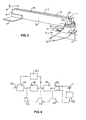
- FIG 3 shows one possible means of mounting piezoelectric bimorph actuator 1 and making electrical connections to it.
- Bimorph 1 is attached to a fibreglass circuit board 9, being inserted into a slot in said circuit board and secured therein with epoxy cement 10 or other appropriate adhesive.
- Circuit board 9 is attached in position onto the entrance aperture of the polychromator or other spectroscopic apparatus (not shown).
- Electrical connection to bimorph 1 is established by means of connecting wires 8 that are soldered to copper contact pads 11 on board 9.
- Electric wires 12 are soldered to pads 11 for connection to a drive circuit such as that of Figure 4 .
- FIG. 4 The circuit diagram of Figure 4 and associated voltage versus time waveforms show how the required driving voltage waveform may be achieved.
- a pulse signal 13 applied to Schmitt trigger pulse squarer 14 produces a square wave 15 that passes to an integrator and limiter 16, producing a trapezoid wave 17. This passes to a sine shaper 18 and generates a quasistatic 'sine' wave 19, which is applied to amplifier 20.
- the output of amplifier 20 drives the piezoelectric bimorph actuator 1 to move the shutter to block (or unblock) the beam for a time determined by the width of pulse 19 and then return it to its original position.
- the microprocessor supervisory device 24 signals the timing and relay drive 25 to close photovoltaic relay 26.
- Relay 26 is closed slowly, through the linear region of its operating characteristics, to ensure that there are no abrupt voltage changes applied to the bimorph 1.
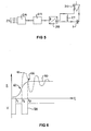
- An alternative piezoelectric excitation voltage sequence involves an initial application of the drive voltage V at time t 1 (see lower voltage (V) versus time (t) trace 38) until the bimorph 1 has moved through approximately half the desired displacement (eg. point 42 on upper displacement ( ⁇ ) versus time (t) trace 40).
- the dashed trace 41 illustrates the decaying oscillation that an undamped bimorph 1 would experience on application of a single step voltage V).
- the polarity of the drive voltage is then reversed at time t 2 to actively decelerate the bimorph 1, so that it reaches the desired position with essentially zero velocity (eg. point 44 on upper trace 40).
- the steady state drive voltage is re-applied to maintain the new position.
- the displacement ⁇ of the bimorph actuator 1 approximates much more closely to a step function, as the trace 40 in Fig. 6 shows.
- the circuit diagram of Fig 7 and associated voltage traces Figs. 8A-E show how the required alternative excitation damping voltage waveform may be practically achieved.
- the circuit of Fig. 7 comprises inverters 46, 48, OR gates 50, 56 and monostables 52, 54.
- the traces A-E correspond to voltage versus time signals at the positions marked A-E on the circuit of Fig. 7 .
- Trace A of Fig. 8 represents the applied drive signal to actuate the shutter device 1 between times t 1 and t' 1
- trace E of Fig. 8 denotes the actual drive to piezoelectric actuator 1, utilising the excitation sequence explained above.
- Monostable elements 52 and 54 provide the voltage switching periods as triggered by the applied drive signal A, the sequence t 1 -t 3 showing the drive signal for actuating piezoelectric actuator 1 into its shuttering position, whilst the sequence t' 1 -t' 3 represents the drive in the reverse direction for actuator 1 to recover its at-rest position.
- Figure 9A shows the bimorph 1 in a first position in which light rays 28 and 29 are allowed to enter the entrance aperture 32 of a spectroscopic instrument (not shown). Rays 28 and 29 indicate the effective optical entrance beam of said spectroscopic instrument, while rays 30 and 31 indicate the edges of the beam from the light source (not shown) focussed onto the plane of entrance aperture 32.
- Figure 9B shows bimorph 1 in a second position in which shutter element 7 prevents light rays 28 and 29 from entering entrance aperture 32, but rays 30 and 31 striking the surface 33 surrounding the entrance aperture 32 may be reflected or scattered from said surface 33 onto the proximate surface of shutter element 7 and thence into the entrance aperture 32.
- Figures 10A and 10B show how masks 34 and 35 placed between a source (not shown) of light rays 28, 29, 30 and 31 prevent light from striking the surface 33 around entrance aperture 32.
- Rays 28 and 29 indicate the effective optical entrance beam of a spectroscopic instrument (not shown), while rays 30 and 31 indicate the extreme edges of the light beam from said source focussed onto the plane of entrance aperture 32.
- Mask 35 includes an aperture 36 having a size just greater than that of the effective optical entrance beam at that location, said optical entrance beam being indicated by light rays 28 and 29.
- Figure 10A shows the bimorph 1 in a first position in which light rays 28 and 29 are allowed to enter the entrance aperture 32 of a spectroscopic instrument (not shown).
- Figure 10B shows bimorph 1 in a second position in which shutter element 7 prevents light rays 28 and 29 from entering entrance aperture 32, and at the same time rays 30 and 31 are prevented from striking the surface 33 surrounding the entrance aperture 32 by masks 34 and 35. Consequently the problem indicated in Figure 9B of light entering entrance aperture 32 by reflection or scattering from surface 33 and the proximate surface of shutter 7 is avoided.
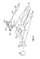
- An example of spectroscopy apparatus namely an optical emission spectrometer as illustrated by Fig. 11 , comprises a spectroscopic light source 60 which emits spectral light of a sample 62.
- Light source 60 in a preferred embodiment is an inductively coupled plasma but may be any other spectroscopic light source adapted to emitting light of spectroscopic interest (i.e. spectral light of a sample).
- Spectral light 62 emitted by spectroscopic light source 60 falls on mirror 64.
- mirror 62 be provided with adjustment means (not shown) so that light can be selected according to its spatial origin within spectroscopic light source 60.
- Spectral light 62 is reflected from mirror 64 onto a focussing mirror 66.
- the spectral light 62 then strikes a folding mirror 68 and is thereby directed onto aperture 70, onto which it is focused by the action of focussing mirror 66.
- a shutter device 72 as above described is so located with respect to aperture 70 that the shutter 72 can selectively be moved to a first position in which it obstructs spectral light 62 or to a second position in which spectral light 62 passes without obstruction.
- the spectral light 62 passes through aperture 70 and falls on a first polychromator focussing mirror 74 which focuses the spectral light 62 through an order-separating prism 76 and onto an echelle grating 78.
- Light reflected from echelle grating 78 has been spatially separated in a first direction according to wavelength but a plurality of spectral orders are spatially superimposed, as is known to those skilled in the art.
- order-separating prism 76 the spectral light 62 is spatially separated in a second direction according to wavelength. The light 62 then strikes a second polychromator focussing mirror 80 which focuses it onto an array detector 82.
- An image of aperture 70 is formed on array detector 82 at a spatial position that is determined by the wavelength of the light.
- Array detector 82 is provided with a large plurality of light-detecting elements (pixels) that convert, by known means, incident light intensity into an electrical charge proportional to the intensity of the incident light.
- intensity measurements are converted to measurements of the concentration of specific chemical elements by reference to measurements made when samples having known concentrations of said chemical elements are subjected to the measuring process.
- the shutter device 72 is operated by application of an electrical signal to its piezoelectric structure to move the shutter to the first position to prevent the spectral light 62 from reaching the detector 82.
- This allows a plurality of the elements of the detector 82 to be serially read by the means 84 whilst the detector 82 is shielded from the spectral light 62.
- Fig. 11 shows spectroscopy apparatus for spectrochemical analysis of a sample which comprises a light source and a system for interacting the light source and a sample 60 for providing spectral light 62 of the sample.
- the optical system of the spectroscopy apparatus includes a polychromator 70, 74-78 and the multi-element solid state detector 82.
- the apparatus also includes means 84 for serially reading a plurality of the elements of the detector to provide light intensity measurements.
- light 92 is emitted by light source 90, which in a preferred embodiment is a hollow cathode lamp but which may be any other spectroscopic light source adapted to emitting light capable of being absorbed by a sample 98 in an absorption cell 96.
- Absorption cell 96 may be a chemical flame, a furnace, a glass cell, or any other device capable of containing a sample 97 of spectroscopic interest for exposure to light 92.
- the light 92 is focussed into absorption cell 96 by focussing means 94.
- Focussing means 94 may be a lens or a mirror or a plurality or combination thereof.
- a representative portion 97 of said sample is introduced into absorption cell 96 by means as known to those skilled in the art, and is therein caused to absorb light at specific wavelengths.
- the extent of absorption at specific wavelengths is indicative of the chemical composition of said sample.
- the light 98 exiting the absorption cell 96 is the spectral light of the sample as hereinbefore defined. Measurements of light absorption at specific wavelengths are converted to measurements of the concentration of specific chemical species of interest by reference to measurements made when samples having known concentrations of said chemical species are subjected to the measurement process.
- Measurement of the electric charges generated at specific spatial positions on array detector 82 provides a measurement of the intensities of light of specific wavelengths.
- intensity measurements are readily converted to absorption measurements by reference to intensity measurements made when a sample containing essentially none of the chemical species of interest is placed in absorption cell 96.
- the invention that has been described is applicable for use with various types of spectroscopic techniques such as, for example, optical emission spectrometry with an inductively coupled plasma source. It is also applicable to emission spectrometry with any other appropriate light sources including but not limited to electrical arcs, electrical sparks, plasma, glow discharges and flames. Furthermore, the invention is applicable to any spectroscopic apparatus or instrument that might require the rapid and reproducible blocking and unblocking of an optical path.
- the invention has been described with reference to the use of a single shutter having a bimorph actuator serving to block and unblock an optical path, but clearly a number of such shutters may be used together and operable to block different optical paths or different parts of an image area.
- the invention which has been described preferably makes the use of a piezoelectric bimorph arranged as a cantilever, in which the free end moves along an arc, but other configurations are possible.
- a piezoelectric bimorph might be configured as a simple beam, in which the centre of the beam moves up and down. In such a configuration the deflection is only 25% of that achievable from a beam of the same dimensions configured as a cantilever but the force exerted is 4 times greater.
- a piezoelectric bimorph might be configured as an 's' beam, in which the free end moves linearly.
Landscapes
- Physics & Mathematics (AREA)
- Spectroscopy & Molecular Physics (AREA)
- General Physics & Mathematics (AREA)
- Spectrometry And Color Measurement (AREA)
- Investigating Or Analysing Materials By Optical Means (AREA)
Claims (14)
- Appareil de spectroscopie pour l'analyse spectrochimique d'un échantillon comprenant :une source de lumière (60) ;un système pour faire interagir la source de lumière avec un échantillon pour fournir la lumière spectrale (62) de l'échantillon ;un système optique (64-66-68) comprenant un polychromateur (70,74-80) ;un détecteur à semi-conducteurs à éléments multiples (82) pour fournir des mesures d'intensité de la lumière spectrale en fonction de la longueur d'onde ;des moyens (84) pour lire en série une pluralité des éléments du détecteur (82) pour fournir lesdites mesures d'intensité de lumière ;un dispositif d'obturation (72) ayant une structure piézoélectrique (2,3) et pouvant fonctionner lors de l'application d'un signal électrique (38) pour un déplacement entre deux positions, dans lequel, dans une position, la lumière spectrale (62) est autorisée à atteindre le détecteur (82), et, dans l'autre position, la lumière spectrale (62) est empêchée d'atteindre le détecteur (82) pour que la pluralité d'éléments de détecteur soient lus en série alors que le détecteur est protégé de la lumière spectrale ; etun circuit électrique pour fournir ledit signal électrique (38) à la structure piézoélectrique, le circuit fournissant un profil de tension en fonction du temps (38) qui d'abord accélère (42) le dispositif d'obturation vers sa position d'actionnement et le décélère ensuite de sorte qu'il atteigne sa position d'actionnement avec une vitesse sensiblement nulle (44).
- Appareil de spectroscopie selon la revendication 1, dans lequel la structure piézoélectrique du dispositif d'obturation est un bimorphe (1).
- Appareil de spectroscopie selon la revendication 2, dans lequel le bimorphe (1) est monté (9-10) en porte-à-faux avec une extrémité libre (6) qui se déplace le long d'un arc pour ledit déplacement entre ladite une position et ladite une autre position.
- Appareil de spectroscopie selon la revendication 2 ou la revendication 3, dans lequel le bimorphe (1) comprend deux bandes de matériau piézoélectrique (2,3) liées aux faces opposées d'un substrat souple (4).
- Appareil de spectroscopie selon la revendication 4, dans lequel le substrat souple (4) est un composite en fibre de carbone.
- Appareil de spectroscopie selon l'une quelconque des revendications 1 à 5, dans lequel le dispositif d'obturation (72) comprend un élément d'obturation (7) fixé à la structure piézoélectrique et qui est déplacé par la structure piézoélectrique pour définir ladite une position et ladite une autre position dans lesquelles l'élément d'obturation bloque ou ne bloque pas ladite lumière spectrale.
- Appareil de spectroscopie selon l'une quelconque des revendications 1 à 6, dans lequel ledit déplacement du dispositif d'obturation (72) définit un plan de déplacement et l'agencement du système optique (64-66-68) est tel que ladite lumière spectrale (62) se propage sensiblement à angle droit par rapport au dit plan de déplacement.
- Appareil de spectroscopie selon l'une quelconque des revendications 1 à 7, dans lequel le dispositif d'obturation (72) est positionné de sorte qu'il bloque et ne bloque pas la lumière spectrale adjacente à une ouverture d'entrée (70) du polychromateur.
- Appareil de spectroscopie selon la revendication 8, comprenant un masque (35) positionné entre le dispositif d'obturation et la source de lumière pour ne permettre qu'à la lumière spectrale correspondant au faisceau d'entrée optique efficace du polychromateur d'atteindre le dispositif d'obturation.
- Appareil de spectroscopie selon la revendication 9, comprenant un deuxième masque (34) positionné entre le dispositif d'obturation et le premier masque défini pour éviter l'entrée d'une lumière spectrale réfléchie dans l'ouverture d'entrée du polychromateur lorsque le dispositif d'obturation bloque la lumière spectrale.
- Appareil de spectroscopie selon l'une quelconque des revendications 1 à 10, dans lequel le circuit électrique comprend des éléments de circuit de protection (22) qui empêchent l'application de toutes tensions transitoires à la structure piézoélectrique.
- Appareil de spectroscopie selon la revendication 11, dans lequel les éléments de circuit de protection comprennent un dispositif (24) pour surveiller le signal électrique appliqué à la structure piézoélectrique (1) et un élément à résistance élevée (27), dans lequel les éléments de circuit de protection peuvent être mis en oeuvre pour que l'élément à résistance élevée (27) soit normalement shunté et pour qu'il soit interposé en série avec la structure piézoélectrique (1) lors de la détection d'une tension transitoire par le dispositif de surveillance.
- Appareil de spectroscopie selon l'une quelconque des revendications 1 à 12, dans lequel le détecteur à semi-conducteurs à éléments multiples (82) est un dispositif de transfert de charges qui est un dispositif d'injection de charges (CID) ou un dispositif à couplage de charges (CCD).
- Appareil de spectroscopie selon la revendication 13, dans lequel les éléments du détecteur sont agencés en tant qu'ensemble régulier de rangées et de colonnes.
Applications Claiming Priority (5)
| Application Number | Priority Date | Filing Date | Title |
|---|---|---|---|
| AUPQ5653A AUPQ565300A0 (en) | 2000-02-15 | 2000-02-15 | Optical shutter for a spectroscopy instrument |
| AUPQ565300 | 2000-02-15 | ||
| AUPQ9273A AUPQ927300A0 (en) | 2000-08-08 | 2000-08-08 | Optical shutter for a spectroscopy instrument |
| AUPQ927300 | 2000-08-08 | ||
| PCT/AU2001/000147 WO2001061291A1 (fr) | 2000-02-15 | 2001-02-15 | Obturateur optique pour instrument de spectroscopie |
Publications (3)
| Publication Number | Publication Date |
|---|---|
| EP1169623A1 EP1169623A1 (fr) | 2002-01-09 |
| EP1169623A4 EP1169623A4 (fr) | 2006-07-05 |
| EP1169623B1 true EP1169623B1 (fr) | 2013-12-18 |
Family
ID=25646260
Family Applications (1)
| Application Number | Title | Priority Date | Filing Date |
|---|---|---|---|
| EP01905489.9A Expired - Lifetime EP1169623B1 (fr) | 2000-02-15 | 2001-02-15 | Obturateur optique pour instrument de spectroscopie |
Country Status (4)
| Country | Link |
|---|---|
| US (1) | US6753959B2 (fr) |
| EP (1) | EP1169623B1 (fr) |
| JP (1) | JP2003523509A (fr) |
| WO (1) | WO2001061291A1 (fr) |
Families Citing this family (20)
| Publication number | Priority date | Publication date | Assignee | Title |
|---|---|---|---|---|
| DE10131684C1 (de) * | 2001-06-29 | 2002-12-12 | Zeiss Carl Jena Gmbh | Vorrichtung und Verfahren zur ortsaufgelösten Messung einer Schichtdicke |
| US7106826B2 (en) * | 2002-01-07 | 2006-09-12 | Cdex, Inc. | System and method for adapting a software control in an operating environment |
| AU2003299556A1 (en) * | 2002-11-13 | 2004-06-03 | Proportional Technologies, Inc. | Boron coated straw neutron detector |
| US20040155202A1 (en) * | 2002-11-21 | 2004-08-12 | Cdex, Inc. | Methods and apparatus for molecular species detection, inspection and classification using ultraviolet fluorescence |
| US7154102B2 (en) * | 2002-11-21 | 2006-12-26 | Cdex, Inc. | System and methods for detection and identification of chemical substances |
| DE102005008889B4 (de) * | 2005-02-26 | 2016-07-07 | Leybold Optics Gmbh | Optisches Monitoringsystem für Beschichtungsprozesse |
| US8148874B2 (en) * | 2005-04-15 | 2012-04-03 | University Of Florida Research Foundation, Inc. | Microactuator having multiple degrees of freedom |
| US7586602B2 (en) | 2006-07-24 | 2009-09-08 | General Electric Company | Method and apparatus for improved signal to noise ratio in Raman signal detection for MEMS based spectrometers |
| US7381972B1 (en) | 2006-07-24 | 2008-06-03 | Science Applications International Corporation | System and method for light fluorescence detection |
| US7681290B2 (en) * | 2006-10-20 | 2010-03-23 | The Boeing Company | Piezoelectric bimorph beam manufacturing method |
| US7852472B1 (en) * | 2007-07-17 | 2010-12-14 | Johnson William M | Systems and methods for spectroscopy using opposing laser beams |
| NL1036184A1 (nl) * | 2007-12-05 | 2009-06-08 | Asml Netherlands Bv | Inspection apparatus, lithographic apparatus and method of measuring a property of a substrate. |
| CN106331442B (zh) | 2015-07-02 | 2021-01-15 | 松下知识产权经营株式会社 | 摄像装置 |
| US10866139B2 (en) * | 2018-08-10 | 2020-12-15 | Perkinelmer Health Sciences, Inc. | Spectrometers with retro-reflective surfaces and related instruments |
| RU2686386C1 (ru) * | 2018-09-28 | 2019-04-25 | Акционерное общество "Научно-исследовательский институт "Полюс" им. М.Ф. Стельмаха" | Оптический приемник |
| RU2688947C1 (ru) * | 2018-09-28 | 2019-05-23 | Акционерное общество "Научно-исследовательский институт "Полюс" им. М.Ф. Стельмаха" | Фотоприемное устройство с затвором |
| RU2686406C1 (ru) * | 2018-09-28 | 2019-04-25 | Акционерное общество "Научно-исследовательский институт "Полюс" им. М.Ф. Стельмаха" | Приемник лазерного излучения |
| RU2690718C1 (ru) * | 2018-09-28 | 2019-06-05 | Акционерное общество "Научно-исследовательский институт "Полюс" им. М.Ф. Стельмаха" | Приемник оптического излучения |
| CN109632766A (zh) * | 2019-01-10 | 2019-04-16 | 中国原子能科学研究院 | 一种火花光源与二维中阶梯光路相结合的光谱分析系统 |
| JP7219096B2 (ja) | 2019-01-21 | 2023-02-07 | 浜松ホトニクス株式会社 | 分光測定装置および分光測定方法 |
Family Cites Families (14)
| Publication number | Priority date | Publication date | Assignee | Title |
|---|---|---|---|---|
| US4214835A (en) * | 1979-01-02 | 1980-07-29 | Baird Corporation | Spectrometer sequential readout system |
| US4647199A (en) * | 1984-09-14 | 1987-03-03 | The Perkin-Elmer Corporation | Automatic shutter system |
| JPS61195858A (ja) * | 1985-02-25 | 1986-08-30 | Tadashi Sekiguchi | プリンタ装置のプリンタヘツド |
| JPH01235389A (ja) * | 1988-03-16 | 1989-09-20 | Copal Co Ltd | 電圧素子の駆動方法 |
| JP2514851Y2 (ja) * | 1988-04-08 | 1996-10-23 | 第一電子工業 株式会社 | コネクタのロック手段 |
| EP0366847A3 (fr) * | 1988-11-02 | 1991-01-09 | Sportsoft Systems, Inc. | Système de visualisation graphique avec des éléments bimorphes |
| US5245176A (en) * | 1992-06-10 | 1993-09-14 | Akzo N.V. | Method for scanning photodiodes utilizing a shutter mechanism having opening and closing transition times |
| US5412468A (en) * | 1993-03-09 | 1995-05-02 | The Perkin-Elmer Corporation | Grouping of spectral bands for data acquisition in a spectrophotometer |
| US5477321A (en) * | 1994-08-31 | 1995-12-19 | Bayer Corporation | Dual beam tunable spectrometer |
| US5796522A (en) * | 1996-12-20 | 1998-08-18 | Eastman Kodak Company | Lenslet array system with a baffle structure and a shutter |
| US5781331A (en) * | 1997-01-24 | 1998-07-14 | Roxburgh Ltd. | Optical microshutter array |
| JP2953426B2 (ja) * | 1997-05-01 | 1999-09-27 | 日本電気株式会社 | Lsi製造用プロセス装置 |
| JPH11142240A (ja) * | 1997-11-11 | 1999-05-28 | Jasco Corp | 分光装置 |
| JPH11261899A (ja) * | 1998-03-12 | 1999-09-24 | Canon Inc | 固体撮像装置 |
-
2001
- 2001-02-15 US US09/958,448 patent/US6753959B2/en not_active Expired - Lifetime
- 2001-02-15 WO PCT/AU2001/000147 patent/WO2001061291A1/fr not_active Ceased
- 2001-02-15 EP EP01905489.9A patent/EP1169623B1/fr not_active Expired - Lifetime
- 2001-02-15 JP JP2001560637A patent/JP2003523509A/ja active Pending
Also Published As
| Publication number | Publication date |
|---|---|
| EP1169623A1 (fr) | 2002-01-09 |
| US6753959B2 (en) | 2004-06-22 |
| EP1169623A4 (fr) | 2006-07-05 |
| JP2003523509A (ja) | 2003-08-05 |
| WO2001061291A1 (fr) | 2001-08-23 |
| US20040085535A1 (en) | 2004-05-06 |
Similar Documents
| Publication | Publication Date | Title |
|---|---|---|
| EP1169623B1 (fr) | Obturateur optique pour instrument de spectroscopie | |
| JP4076077B2 (ja) | アクティブ・マトリクス光学系を用いた分光計 | |
| JP4368082B2 (ja) | テラヘルツ波分光器 | |
| US9903758B2 (en) | Spectral measurement device and analysis apparatus | |
| US6724950B2 (en) | Electro-optically tunable filter with mesh structure to filter optical signal | |
| US12163834B2 (en) | Micro wideband spectroscopic analysis device | |
| US7728973B2 (en) | Line camera for spectral imaging | |
| US20070177145A1 (en) | Optical spectrum analyzer | |
| US6853449B2 (en) | Programmable diffraction grating sensor | |
| JP6805758B2 (ja) | スペクトル測定器及び分析装置 | |
| US6813019B2 (en) | Method and apparatus for spectrochemical analysis | |
| He et al. | Imaging spectrometer based on AOTF and its prospects in deep-space exploration application | |
| KR950008824B1 (ko) | 방사선 분석용 홀로그래픽 분광계 및 이의 분석 방법 | |
| AU767168B2 (en) | Optical shutter for spectroscopy instrument | |
| Grueger et al. | Realization of a spectrometer with micromachined scanning grating | |
| FI82863B (fi) | Spektrometriskt foerfarande och spektrometer. | |
| RU2186351C1 (ru) | Устройство для измерения физических параметров, преимущественно температуры | |
| US20110130969A1 (en) | Resonant-Wavelength Measurement Method For Label-Independent Scanning Optical Reader | |
| Norkus et al. | High-resolution pyroelectric linear arrays based on LiTaO3 | |
| Beddows et al. | Application of frustrated total internal reflection devices to analytical laser spectroscopy | |
| Gagnon et al. | Multiband sensor using thick holographic gratings for sulfur detection by laser-induced breakdown spectroscopy | |
| JP7544382B2 (ja) | 静電気センサ | |
| KR101490884B1 (ko) | 구동형 마이크로 그레이팅 및 이를 이용하는 상관 분광기 | |
| RU2186350C1 (ru) | Устройство для измерения температуры | |
| Chao et al. | Compact liquid crystal waveguide Fourier transform spectrometer for real-time gas sensing in NIR spectral band |
Legal Events
| Date | Code | Title | Description |
|---|---|---|---|
| PUAI | Public reference made under article 153(3) epc to a published international application that has entered the european phase |
Free format text: ORIGINAL CODE: 0009012 |
|
| 17P | Request for examination filed |
Effective date: 20011025 |
|
| AK | Designated contracting states |
Kind code of ref document: A1 Designated state(s): DE FR GB |
|
| A4 | Supplementary search report drawn up and despatched |
Effective date: 20060606 |
|
| 17Q | First examination report despatched |
Effective date: 20070504 |
|
| RAP1 | Party data changed (applicant data changed or rights of an application transferred) |
Owner name: AGILENT TECHNOLOGIES AUSTRALIA (M) PTY LTD |
|
| GRAP | Despatch of communication of intention to grant a patent |
Free format text: ORIGINAL CODE: EPIDOSNIGR1 |
|
| INTG | Intention to grant announced |
Effective date: 20130725 |
|
| GRAS | Grant fee paid |
Free format text: ORIGINAL CODE: EPIDOSNIGR3 |
|
| GRAA | (expected) grant |
Free format text: ORIGINAL CODE: 0009210 |
|
| AK | Designated contracting states |
Kind code of ref document: B1 Designated state(s): DE FR GB |
|
| REG | Reference to a national code |
Ref country code: GB Ref legal event code: FG4D |
|
| REG | Reference to a national code |
Ref country code: DE Ref legal event code: R096 Ref document number: 60148500 Country of ref document: DE Effective date: 20140213 |
|
| PGFP | Annual fee paid to national office [announced via postgrant information from national office to epo] |
Ref country code: FR Payment date: 20140211 Year of fee payment: 14 |
|
| PGFP | Annual fee paid to national office [announced via postgrant information from national office to epo] |
Ref country code: GB Payment date: 20140212 Year of fee payment: 14 |
|
| REG | Reference to a national code |
Ref country code: DE Ref legal event code: R097 Ref document number: 60148500 Country of ref document: DE |
|
| PLBE | No opposition filed within time limit |
Free format text: ORIGINAL CODE: 0009261 |
|
| STAA | Information on the status of an ep patent application or granted ep patent |
Free format text: STATUS: NO OPPOSITION FILED WITHIN TIME LIMIT |
|
| 26N | No opposition filed |
Effective date: 20140919 |
|
| REG | Reference to a national code |
Ref country code: DE Ref legal event code: R097 Ref document number: 60148500 Country of ref document: DE Effective date: 20140919 |
|
| GBPC | Gb: european patent ceased through non-payment of renewal fee |
Effective date: 20150215 |
|
| REG | Reference to a national code |
Ref country code: FR Ref legal event code: ST Effective date: 20151030 |
|
| PG25 | Lapsed in a contracting state [announced via postgrant information from national office to epo] |
Ref country code: GB Free format text: LAPSE BECAUSE OF NON-PAYMENT OF DUE FEES Effective date: 20150215 |
|
| PG25 | Lapsed in a contracting state [announced via postgrant information from national office to epo] |
Ref country code: FR Free format text: LAPSE BECAUSE OF NON-PAYMENT OF DUE FEES Effective date: 20150302 |
|
| PGFP | Annual fee paid to national office [announced via postgrant information from national office to epo] |
Ref country code: DE Payment date: 20180130 Year of fee payment: 18 |
|
| REG | Reference to a national code |
Ref country code: DE Ref legal event code: R119 Ref document number: 60148500 Country of ref document: DE |
|
| PG25 | Lapsed in a contracting state [announced via postgrant information from national office to epo] |
Ref country code: DE Free format text: LAPSE BECAUSE OF NON-PAYMENT OF DUE FEES Effective date: 20190903 |