EP1174733A2 - Optischer Sensor - Google Patents
Optischer Sensor Download PDFInfo
- Publication number
- EP1174733A2 EP1174733A2 EP01117432A EP01117432A EP1174733A2 EP 1174733 A2 EP1174733 A2 EP 1174733A2 EP 01117432 A EP01117432 A EP 01117432A EP 01117432 A EP01117432 A EP 01117432A EP 1174733 A2 EP1174733 A2 EP 1174733A2
- Authority
- EP
- European Patent Office
- Prior art keywords
- optical sensor
- cmos line
- sensor according
- signal values
- elements
- Prior art date
- Legal status (The legal status is an assumption and is not a legal conclusion. Google has not performed a legal analysis and makes no representation as to the accuracy of the status listed.)
- Granted
Links
- 230000003287 optical effect Effects 0.000 title claims abstract description 39
- 238000005259 measurement Methods 0.000 claims description 56
- 238000012432 intermediate storage Methods 0.000 claims description 28
- 238000000034 method Methods 0.000 claims description 4
- 238000012544 monitoring process Methods 0.000 claims description 4
- 238000001514 detection method Methods 0.000 description 12
- 238000011156 evaluation Methods 0.000 description 11
- 230000005540 biological transmission Effects 0.000 description 7
- 238000010586 diagram Methods 0.000 description 4
- 238000003860 storage Methods 0.000 description 4
- 230000005855 radiation Effects 0.000 description 3
- 238000012217 deletion Methods 0.000 description 2
- 230000037430 deletion Effects 0.000 description 2
- 230000000737 periodic effect Effects 0.000 description 2
- 238000012546 transfer Methods 0.000 description 2
- 230000015572 biosynthetic process Effects 0.000 description 1
- 238000011161 development Methods 0.000 description 1
- 230000018109 developmental process Effects 0.000 description 1
- 238000009826 distribution Methods 0.000 description 1
- 230000000694 effects Effects 0.000 description 1
- 230000005484 gravity Effects 0.000 description 1
- 230000001795 light effect Effects 0.000 description 1
- 238000004519 manufacturing process Methods 0.000 description 1
- 238000007493 shaping process Methods 0.000 description 1
- 230000001629 suppression Effects 0.000 description 1
- 230000001360 synchronised effect Effects 0.000 description 1
- 230000001960 triggered effect Effects 0.000 description 1
- 238000011144 upstream manufacturing Methods 0.000 description 1
Images




Classifications
-
- G—PHYSICS
- G01—MEASURING; TESTING
- G01V—GEOPHYSICS; GRAVITATIONAL MEASUREMENTS; DETECTING MASSES OR OBJECTS; TAGS
- G01V8/00—Prospecting or detecting by optical means
- G01V8/10—Detecting, e.g. by using light barriers
- G01V8/20—Detecting, e.g. by using light barriers using multiple transmitters or receivers
Definitions
- the invention relates to an optical sensor according to the preamble of the claim 1.
- Such sensors are designed as light scanners and have a transmitted light beam emitting transmitter and receiving light rays Receivers that are integrated in a common housing.
- the Transmitted light rays emitted by the transmitter are received by the object as received light rays reflected back to the receiver.
- For object detection the reception signals of the receiver are evaluated in an evaluation unit.
- the optical sensor can in particular be a spatially resolving receiver Have detector. From the point of impact of the received light rays on the The receiver can then in the evaluation unit the distance of an object to Sensor can be calculated.
- Such a receiver can in particular from a CCD line with a line-shaped arrangement of CCD line elements. in principle the receiver can also use a CMOS line with a line-shaped arrangement be formed by CMOS line elements.
- a CCD line is in the evaluation unit generates a clock signal with a predetermined clock frequency.
- sequences of start and shutter pulses are generated in the evaluation unit with which the CCD line is controlled.
- the CCD line is in synchronous operation operated.
- the start and shutter pulses are consecutive Time intervals generated which cycle times form.
- such a time interval begins with a start pulse and ends with the following start impulse.
- the signal values are first of the CCD line elements used in the measurement during the previous cycle time were determined, buffered and then completely read out and in transfer the evaluation unit. Then the CCD line elements deactivated by short-circuiting, the contents of the CCD line elements to be deleted.
- the exposure time is special given by the cycle time of the CCD line.
- the exposure time specified via shutter pulses at the end of the exposure time become.
- the CCD row elements generated new signal values whose amplitude distribution over the line length provides a measure of the current distance of the object, from which the received light rays are reflected back to the CCD line.
- a disadvantage of such optical sensors is that at the beginning of each cycle time first reading out the old signal values of the CCD line elements and then the deletion of the contents of all the CCD line element must be done before a new measurement was made during a subsequent exposure time can be.
- This waiting time can be up to a few milliseconds and therefore considerable be longer than the exposure time, which is typically in the microsecond range lies.
- the invention has for its object an optical sensor of the beginning mentioned type so that the response times are as short as possible having.
- the optical sensor according to the invention for detecting objects in one Monitoring area has a transmitter emitting light rays and a receiving light beam receiving receiver.
- the recipient is of at least one asynchronously controlled CMOS line with individually controllable CMOS line elements formed.
- Asynchronous control means that the CMOS line elements can be combined in one asynchronous operation and regardless of cycle times within which Measurements for object detection are carried out by short-circuiting be deactivated. Short-circuiting the CMOS line elements and their Exposure to carry out measurements for object detection can thus take place independently of one another and at freely selectable times.
- the main advantage of the sensor according to the invention is therefore that that there are no waiting times when triggering a measurement for object detection, caused by short-circuiting the CMOS line elements.
- the Exposure times for performing the measurement rather begin immediately with the start of a measurement.
- the response time and thus the measuring time of the The sensor according to the invention is therefore extremely small.
- CMOS line elements are also available at freely selectable times controllable, so that the signal values of individual CMOS line elements can be read out individually and thus can be evaluated individually.
- the readout of the signal values of the CMOS line element can be too free selectable times are interrupted, so that only the signal values a certain number of CCD line elements per readout be read out.
- This asynchronous operation of the CMOS line makes it extremely short Get measurement times. It is particularly advantageous that when starting a Measurement no waiting times arise because the beginning of the exposure time of the CMOS line immediately coincides with the start of a measurement. There with individual CMOS line elements can be addressed in accordance with the measurements as required the respective measurement can be tailored to the respective application conditions adjusted and the measuring time can be shortened further.
- the CMOS line is a Logic circuit assigned. The control takes place with this logic circuit the CMOS line and in particular the specification of the measurement times. Still is assigned at least one intermediate storage unit to the CMOS line, which consists of there is an arrangement of sample and hold elements.
- CMOS line element assigned a sample and hold element, in which the signal value of the corresponding CMOS line element is buffered can be.
- the control of the reading-in and reading-out of signal values in the sample and hold elements are also taken over by the logic circuit.
- CMOS line with the or each buffer unit as well as the logic circuit are preferably integrated on a chip and form a common one integrated circuit, which is inexpensive to manufacture.
- a computer unit is assigned to this integrated circuit Control signals generated and integrated into the components Reads circuit.
- the start times are via the computer units Predeterminable for which individual measurements for object detection are started.
- the signal values are transferred from the intermediate storage unit to the Computer unit read so that there the evaluation of the signal values for Detection of objects in the surveillance area can take place. This is done Before reading into the computer unit, preferably digitizing the signal values by means of an analog / digital converter.
- the CMOS line allocated two buffer units so that each CMOS line element two sample and hold elements are assigned.
- the signal values of two measurements can be temporarily stored in an arrangement be, which are preferably two directly on top of each other following measurements.
- Two such measurements are used in particular to suppress External light effects.
- a first measurement with the transmitter switched on carried out.
- the signal values generated in the CMOS line elements contain the information about the distance of the object.
- these useful signal components are interference signal components due to the environment existing external light sources superimposed.
- the second measurement is carried out with the transmitter switched off, so that the signal values of the CMOS line elements only contain the interference signal components.
- the signal values for each CMOS line element Measurements subtracted.
- the difference thus formed essentially only contains nor the useful signal components, which are in the computer unit for object detection be evaluated.
- the difference is expediently carried out by a hardware circuit that is upstream of the computing unit.
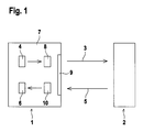
- FIG. 1 shows the optomechanical components of an optical sensor 1 for detecting objects 2 in a surveillance area.
- the sensor 1 has a transmitter light beam 3 emitting transmitter 4 and a receive light beams 5 receiving receiver 6, which in a common Housing 7 are integrated.
- the transmitted light beams 3 are for beam shaping a transmission optics 8 and pass through an exit window 9 in the Front wall of the housing 7 in the monitoring area.
- the transmitted light beams 3 are viewed as an object 2 arranged in the monitoring area Receiving light rays 5 reflected back. Enforce the received light rays 5 the exit window 9 and are via a receiving optics 10 on the Receiver 6 focused.
- FIGS 2 and 3 show two embodiments of the transmitter 4 and the electronic components of the optical sensor connected to the receiver 6 1.
- the transmitter 4 which is designed as a light-emitting diode or as a laser diode, is from a computer unit 11 is controlled and preferably emits transmitted light pulses with a predefinable pulse-pause ratio.
- the computing unit 11 is from a microcontroller, an ASIC or the like educated.
- the receiver 6 is of a CMOS line with a line-shaped arrangement formed by CMOS line elements 6a. Such CMOS lines point a high reception dynamic.
- the received signal dynamics is defined by the ratio of the maximum and minimum amplitudes E max , E min of signal values, which can still be detected by means of the CMOS line elements 6a.
- the reception dynamic range is 10 7 : 1.
- CMOS lines compared to CCD lines, which in principle can also be used as receivers 6 for the optical sensor 1, have a signal evaluation that is up to an order of magnitude fast.
- the CMOS line has a logarithmic characteristic, that is to say the amplitude curve the signal values over the entire amplitude range are logarithmic educated.
- the CMOS line forms a spatially resolving detector, so that by means of the Sensor 1, the distance of an object 2 can be determined.
- the point of impact delivers of the light spot of the received light rays 5 on the CMOS line Measure of the object distance.
- the amplitudes of the signal values at the outputs of the individual CMOS line elements 6a are larger, the stronger the photosensitive surfaces of the CMOS line elements 6a are exposed.
- the calculation of the object distance takes place in the computer unit 11, the signal values of the CMOS line elements 6a preferably the center of gravity of the light spot Receiving light rays 5 is calculated on the CMOS line.
- the CMOS line is a temporary storage unit 12 assigned a linear arrangement of Has sample and hold elements 12a.
- the intermediate storage unit 12 forms a shift register, each with a sample and hold element 12a is assigned to a CMOS line element 6a, so that the signal value thereof CMOS line element 6a in the assigned sample and hold element 12a is temporarily stored.
- the CMOS line and the latch unit 12 is a logic circuit 13 assigned, with all components in the form of an integrated Circuit 14 are integrated on a chip.
- the integrated circuit 14 is connected to the computer unit 11. Of the computer unit 11 sends control signals to the integrated circuit 14 transfer. Conversely, from the intermediate storage unit 12 to predetermined ones Times the temporarily stored signal values in the computer unit 11, in which the object distance is determined from the signal values becomes.
- the analog signal values in the intermediate storage unit 12 are shown in digitized an analog / digital converter 15 before entering the computing unit 11 can be read.
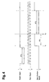
- FIG. 4 shows the time diagrams of various control signals for the arrangement according to FIG. 2.
- 4 transmitter light pulses are emitted by the transmitter with a predetermined pulse-pause ratio.
- a transmitted light pulse emitted by the transmitter 4 is reflected by the object 2 on the CMOS line.
- the signal values registered on the CMOS line elements 6a are evaluated in the computer unit 11 for distance determination.
- the length of each transmitted light pulse essentially defines the measuring time within which the distance is determined.
- the exposure time designated ⁇ t 1 in FIG. 4 is adapted to this measuring time.
- the exposure time ⁇ t 1 represents the time interval within which the CMOS line elements 6a are activated. With continuous light irradiation, the signal value of the exposed CMOS line element 6a increases continuously within the exposure time .DELTA.t 1 and in accordance with the incident light quantity.
- the individual CMOS line elements 6a are deactivated by short-circuiting in the transmission pauses of the transmitter 4 and are thereby deleted.
- the CMOS line elements 6a are short-circuited via the logic circuit 13 in an asynchronous mode.
- a binary reset signal for controlling the CMOS line is generated in the logic circuit 13.
- the reset signal assumes the switching state "0”
- the CMOS line elements 6a are short-circuited.
- the sample and hold elements 12a of the intermediate storage unit 12 are preferably also deleted at the same time. The time interval within which the delete operations took place is denoted by ⁇ t 2 in FIG.
- the CMOS line elements 6a and the sample and hold elements 12a are deleted during ⁇ t 2 asynchronously to the individual exposure times ⁇ t 1 .
- the times at which the deletion processes begin can be specified in the logic circuit 13 or specified via control signals from the computer unit 11, the logic signals 13 being controlled in a suitable manner with the control signals.
- the time intervals ⁇ t 2 are free and can be selected independently of the exposure times ⁇ t 1 .
- the execution of the measurements for object detection is controlled by the computer unit 11.
- the computer unit 11 specifies the transmission clock of the transmitted light pulses.
- the receiver 6 is controlled by the computer unit 11.
- a periodic clock signal is generated by the computer unit 11 and read into the integrated circuit 14.
- 11 binary start / shutter pulses are generated in the computer unit.
- the CMOS line elements 6a are activated, that is to say the duration of a start / shutter pulse defines the exposure time ⁇ t 1 of the CMOS line elements 6a, as can be seen from FIG.
- the exposure time ⁇ t 1 is typically in the range between 0.001 ms and 100 ms. Since the short-circuiting takes place asynchronously and independently of the start / shutter pulses, the start of the exposure time ⁇ t 1 coincides with the start of the start / shutter pulse at t 1 . This means that when a start / shutter pulse is generated, the CMOS line elements 6a are activated immediately without waiting and are ready to carry out a measurement.
- the signal values of the CMOS line elements 6a are stored in the corresponding sample and hold element 12a.
- all or only individual CMOS line elements 6a can be activated and used for the measurement. Accordingly, only the signal values of individual CMOS line elements 6a are read into the assigned sample and hold elements 12a in the latter case.
- the signal values stored in the buffer unit 12 are read out into the computer unit 11.
- a new measurement can then be started with a new start / shutter pulse become. It is advisable to do this before starting a new measurement again short-circuiting the CMOS line elements 6a and deleting the Contents of the sample and hold elements 12a.
- FIG. 3 of the circuit arrangement of the Optical sensor 1 differs from the exemplary embodiment according to Figure 2 essentially in that two identical intermediate storage units 12 each with a line-shaped arrangement of sample and hold elements 12a are provided.
- Buffer units 12 can store the signal values of the CMOS line elements 6a, which are obtained in two different measurements, can be saved separately.
- the contents of the sample and hold elements 12a of both intermediate storage units 12 are analogous to the exemplary embodiment according to FIG. 2 in the computer unit 11 read.
- the analog signal values of the sample and hold elements 12a of each buffer unit 12 in an analog / digital converter 15 digitized.
- the digitized signal values of both intermediate storage units 12 are then fed to a subtractor 16.
- CMOS line elements 6a of both intermediate storage units 12 are formed.
- the differences formed in this way are read into the computer unit 11.
- the Subtractor 16 is from a digital subtractor such as one FPGA or a controller formed. Alternatively, an analog subtracting amplifier be provided, the differences in the contents of the intermediate storage units directly 12 forms. These difference values are then over a Analog / digital converter 15 supplied to the computer unit 11.
- Figure 5 shows the control signals for a first embodiment of a sequence control for the arrangement according to FIG. 3.
- CMOS line elements 6a are short-circuited analogously to the exemplary embodiment according to FIG. 4 via the logic circuit 13 by means of the reset signal during the time intervals ⁇ t 2 .
- the computer unit 11 in turn generates a clock signal to control the integrated circuit 14.
- the computer unit 11 generates separate sequences of start pulses and shutter pulses.
- the exposure time ⁇ t 1 begins with the falling edge of a start pulse, that is to say at this time t 1 the CMOS line elements 6a are activated.
- the exposure time ⁇ t 1 ends at t 2 with the falling edge of the shutter pulse, which begins at the same time as the corresponding start pulse.
- the current signal values which were determined during the previous exposure time ⁇ t 1 , are then read into the now free sample and hold elements 12a of the first buffer unit 12.
- the contents of the intermediate storage unit 12 are read out during the time interval ⁇ t 3 between two start pulses.
- Such an evaluation is also particularly suitable in the event that, in contrast to the embodiment according to FIG. 3, the difference in the contents of the two intermediate storage units 12 is not formed. Instead, the contents of the intermediate storage units 12, which are obtained in two successive measurements, are evaluated separately for rapid signal evaluation. Depending on the application, individual measurements can then be interrupted during the exposure time ⁇ t 1 via the reset signal. The read processes are also reset via the reset signal.
- Figure 6 shows the control signals for a second embodiment of a sequence control for the arrangement according to FIG. 3.
- control signals of the computer unit 11 are analogous to the example shown in FIG 3 formed by the clock signal and start / shutter pulses.
- the pulse durations of the start / shutter pulses in turn define the exposure times ⁇ t 1 .
- the periodic transmitter 4 emits transmitted light pulses with a duration ⁇ t 0 , which corresponds to the exposure time ⁇ t 1 .
- a transmission light pulse is followed by a transmission pause with the duration ⁇ t p .
- the exposure time in each case being ⁇ t 1 .
- the transmitter 4 is switched on in the first measurement, but switched off in the second measurement. Object detection is thus only carried out during the first measurement, which may be falsified by extraneous light radiation.
- the exposure times ⁇ t 1 are selected to be small and are typically between 1 ⁇ s and 10 ⁇ s. In addition, the two measurements follow each other closely. This ensures that the extraneous light radiation does not change or changes only slightly during the measurements.
- the signal values of the CMOS line elements 6a at time t 1 are read into the sample and hold elements 12a of the first buffer unit 12.
- the signal values of the CMOS line elements 6a at time t 2 are read into the sample and hold elements 12a of the second buffer unit 12.
- the contents of the intermediate storage unit 12 are read out during the transmission pause ⁇ t p and fed to the subtractor 16, in which the difference signal of the two measurements is formed.
- the signal values of the corresponding sample and hold elements 12a of the two intermediate storage units 12 are subtracted. The formation of differences almost completely eliminates the influence of extraneous light on the measurements.
- the CMOS line elements 6a In order to rule out measurement falsifications, the CMOS line elements 6a must be deleted during the dead time ⁇ t 4 . For this purpose, short-circuiting of the CMOS line elements 6a is again required, the short-circuiting of the CMOS line elements 6a being carried out automatically by the logic unit.
- the dead time ⁇ t 4 between the measurements becomes undesirably long.
- two receivers 6 can in principle be provided, each of which is formed by a CMOS line and can be controlled via separate reset signals. Then the two measurements can be carried out with different receivers 6, so that the dead time ⁇ t 4 can be chosen to be very short, as shown in FIG.
Landscapes
- Physics & Mathematics (AREA)
- Life Sciences & Earth Sciences (AREA)
- General Life Sciences & Earth Sciences (AREA)
- General Physics & Mathematics (AREA)
- Geophysics (AREA)
- Optical Radar Systems And Details Thereof (AREA)
- Gyroscopes (AREA)
- Glass Compositions (AREA)
- Investigating Or Analysing Materials By The Use Of Chemical Reactions (AREA)
- Geophysics And Detection Of Objects (AREA)
Abstract
Description
- Figur 1:
- Schematische Darstellung der optomechanischen Komponenten des optischen Sensors.
- Figur 2:
- Schematische Darstellung der Elektronikkomponenten eines ersten Ausführungsbeispiels des optischen Sensors.
- Figur 3:
- Schematische Darstellung der Elektronikkomponenten eines zweiten Ausführungsbeispiels des optischen Sensors.
- Figur 4:
- Zeitdiagramme von Steuersignalen für den optischen Sensor gemäß Figur 2.
- Figur 5:
- Zeitdiagramme von Steuersignalen für den optischen Sensor gemäß Figur 3 in einer ersten Betriebsart.
- Figur 6:
- Zeitdiagramme von Steuersignalen für den optischen Sensor gemäß Figur 3 in einer zweiten Betriebsart.
- (1)
- Sensor
- (2)
- Objekt
- (3)
- Sendelichtstrahlen
- (4)
- Sender
- (5)
- Empfangslichtstrahlen
- (6)
- Empfänger
- (6a)
- CMOS-Zeilenelement
- (7)
- Gehäuse
- (8)
- Sendeoptik
- (9)
- Austrittsfenster
- (10)
- Empfangsoptik
- (11)
- Rechnereinheit
- (12)
- Zwischenspeichereinheit
- (12a)
- Sample- and Hold-Element
- (13)
- Logikschaltung
- (14)
- Schaltung
- (15)
- Analog/Digital-Wandler
- (16)
- Subtrahierglied
Claims (21)
- Optischer Sensor zum Erfassen von Objekten in einem Überwachungsbereich mit einem Sendelichtstrahlen emittierenden Sender und einem Empfangslichtstrahlen empfangenden Empfänger, dadurch gekennzeichnet, dass der Empfänger (6) von wenigstens einer asynchron gesteuerten CMOS-Zeile mit einzeln ansteuerbaren CMOS-Zeilenelementen (6a) gebildet ist.
- Optischer Sensor nach Anspruch 1, dadurch gekennzeichnet, dass der CMOS-Zeile eine Logikschaltung (13) zugeordnet ist, mittels derer die CMOS-Zeilenelemente (6a) durch Kurzschließen zu vorgebbaren Zeiten deaktivierbar sind.
- Optischer Sensor nach Anspruch 2, dadurch gekennzeichnet, dass über die Logikschaltung (13) einzelne CMOS-Zeilenelemente (6a) auslesbar sind.
- Optischer Sensor nach einem der Ansprüche 1 - 3, dadurch gekennzeichnet, dass der CMOS-Zeile wenigstens eine Zwischenspeichereinheit (12), bestehend aus einer Anordnung von Sample- and Hold-Elementen (12a) zugeordnet ist, wobei jeweils einem CMOS-Zeilenelement (6a) ein Sample- and Hold-Element (12a) zugeordnet ist, in welches der Signalwert des zugeordneten CMOS-Zeilenelements (6a) einlesbar ist.
- Optischer Sensor nach Anspruch 4, dadurch gekennzeichnet, dass der CMOS-Zeile zwei Zwischenspeichereinheiten (12) zugeordnet sind, wobei jeweils ein Sample- and Hold-Element (12a) beider Zwischenspeichereinheiten (12) einem CMOS-Zeilenelement (6a) zugeordnet ist.
- Optischer Sensor nach Anspruch 5, dadurch gekennzeichnet, dass in den Zwischenspeichereinheiten (12) die bei zu verschiedenen Zeiten erfolgten Messungen generierten Signalwerte der CMOS-Zeilenelemente (6a) abspeicherbar sind.
- Optischer Sensor nach einem der Ansprüche 4 - 6, dadurch gekennzeichnet, dass die Einlesevorgänge zum Einlesen von Signalwerten der CMOS-Zeilenelemente (6a) in die Sample- and Hold-Elemente (12a) der Zwischenspeichereinheiten (12) zu vorgebbaren Zeiten durch die Logikschaltung (13) rücksetzbar sind.
- Optischer Sensor nach einem der Ansprüche 2 - 7, dadurch gekennzeichnet, dass die CMOS-Zeile, die Logikschaltung (13) sowie die oder jede Zwischenspeichereinheit (12) Bestandteile einer integrierten Schaltung (14) sind.
- Optischer Sensor nach einem der Ansprüche 4 - 8, dadurch gekennzeichnet, dass die in der oder jeder Zwischenspeichereinheit (12) gespeicherten Signalwerte in eine Rechnereinheit (11) einlesbar sind.
- Optischer Sensor nach Anspruch 9, dadurch gekennzeichnet, dass die Signalwerte in einer Zwischenspeichereinheit (12) über einen Analog/Digital-Wandler (15) in die Rechnereinheit (11) eingelesen werden.
- Optischer Sensor nach einem der Ansprüche 9 - 10, dadurch gekennzeichnet, dass die Signalwerte entsprechender Sample- and Hold-Elemente (12a) zweier Zwischenspeichereinheiten (12) über ein Subtrahierglied (16) in die Rechnereinheit (11) eingelesen werden.
- Optischer Sensor nach Anspruch 11, dadurch gekennzeichnet, dass dem Subtrahierglied (16) Signalwerte zweier aufeinander folgender Messungen zugeführt werden, wobei in der ersten Zwischenspeichereinheit (12) die bei einer ersten Messung bei aktiviertem Sender (4) erhaltenen Signalwerte abgespeichert sind, und wobei in der zweiten Zwischenspeichereinheit (12) die bei einer zweiten Messung bei deaktiviertem Sender (4) erhaltenen Signalwerte abgespeichert sind.
- Optischer Sensor nach einem der Ansprüche 9 - 12, dadurch gekennzeichnet, dass die CMOS-Zeile, die oder jede Zwischenspeichereinheit (12) sowie die Logikschaltung (13) mit einem in der Rechnereinheit (11) generierten Taktsignal beaufschlagt sind.
- Optischer Sensor nach Anspruch 13, dadurch gekennzeichnet, dass in der Rechnereinheit (11) Folgen von Start-Impulsen und/oder Folgen von Shutter-Impulsen zur Ansteuerung der Logikschaltung (13), der CMOS-Zeile und/oder der oder jeder Zwischenspeichereinheit (12) generiert werden.
- Optischer Sensor nach Anspruch 14, dadurch gekennzeichnet, dass mittels eines Start-Impulses und/oder eines Shutter-Impulses die CMOS-Zeilenelemente (6a) der CMOS-Zeile für eine vorgegebene Belichtungszeit (Δt1) zur Durchführung einer Messung aktivierbar sind, wobei die Belichtungszeit (Δt1) unmittelbar mit einem Start- und/oder Shutter-Impuls beginnt.
- Optischer Sensor nach Anspruch 15, dadurch gekennzeichnet, dass die Dauer der Belichtungszeit (Δt1) über die Rechnereinheit (11) vorgebbar ist.
- Optischer Sensor nach einem der Ansprüche 15 oder 16, dadurch gekennzeichnet, dass zwischen zwei aufeinander folgenden Belichtungszeiten (Δt1) eine Totzeit (Δt4) liegt, innerhalb derer die CMOS-Zeilenelemente (6a) durch Kurzschließen deaktivierbar sind.
- Optischer Sensor nach einem der Ansprüche 15 - 17, dadurch gekennzeichnet, dass die Dauer der Belichtungszeit (Δt1) im Bereich zwischen 1µs und 100 ms liegt.
- Optischer Sensor nach Anspruch 18, dadurch gekennzeichnet, dass die Dauer der Belichtungszeit (Δt1) über die Rechnereinheit (11) vorgebbar ist.
- Optischer Sensor nach einem der Ansprüche 1 - 19, dadurch gekennzeichnet, dass mit diesem eine Distanzmessung durchgeführt wird.
- Optischer Sensor nach Anspruch 20, dadurch gekennzeichnet, dass zur Bestimmung der Distanz aus den Signalwerten der CMOS-Zeilenelemente (6a) die Lage des Lichtflecks der Empfangslichtstrahlen (5) auf der CMOS-Zeile berechnet wird.
Applications Claiming Priority (2)
| Application Number | Priority Date | Filing Date | Title |
|---|---|---|---|
| DE10035465 | 2000-07-21 | ||
| DE10035465 | 2000-07-21 |
Publications (3)
| Publication Number | Publication Date |
|---|---|
| EP1174733A2 true EP1174733A2 (de) | 2002-01-23 |
| EP1174733A3 EP1174733A3 (de) | 2003-05-02 |
| EP1174733B1 EP1174733B1 (de) | 2005-02-02 |
Family
ID=7649679
Family Applications (1)
| Application Number | Title | Priority Date | Filing Date |
|---|---|---|---|
| EP01117432A Expired - Lifetime EP1174733B1 (de) | 2000-07-21 | 2001-07-19 | Optischer Sensor |
Country Status (3)
| Country | Link |
|---|---|
| EP (1) | EP1174733B1 (de) |
| AT (1) | ATE288590T1 (de) |
| DE (1) | DE50105230D1 (de) |
Cited By (19)
| Publication number | Priority date | Publication date | Assignee | Title |
|---|---|---|---|---|
| DE102004053219B3 (de) * | 2004-11-04 | 2006-04-06 | Leuze Electronic Gmbh & Co Kg | Optischer Sensor |
| EP1921587A1 (de) * | 2006-11-09 | 2008-05-14 | Sick Ag | Optoelektronische Überwachungsvorrichtung mit Testeinheit und Testverfahren |
| EP1927867A1 (de) | 2006-12-02 | 2008-06-04 | Sick Ag | Optoelektronischer Mehrebenensensor und Verfahren zur Erfassung von Objekten |
| US8803065B2 (en) | 2010-07-02 | 2014-08-12 | Pantron Instruments Gmbh | Light barrier and method for pulsed operation in which the incidence of extraneous light on the detector can be detected and compensated for |
| DE102004042724B4 (de) * | 2003-09-10 | 2014-08-28 | Baumer Electric Ag | Vorrichtung und Verfahren zur Minimierung von Fremdlichteinflüssen bei einer Messeinrichtung |
| USRE48490E1 (en) | 2006-07-13 | 2021-03-30 | Velodyne Lidar Usa, Inc. | High definition LiDAR system |
| US10983218B2 (en) | 2016-06-01 | 2021-04-20 | Velodyne Lidar Usa, Inc. | Multiple pixel scanning LIDAR |
| US11073617B2 (en) | 2016-03-19 | 2021-07-27 | Velodyne Lidar Usa, Inc. | Integrated illumination and detection for LIDAR based 3-D imaging |
| US11082010B2 (en) | 2018-11-06 | 2021-08-03 | Velodyne Lidar Usa, Inc. | Systems and methods for TIA base current detection and compensation |
| US11137480B2 (en) | 2016-01-31 | 2021-10-05 | Velodyne Lidar Usa, Inc. | Multiple pulse, LIDAR based 3-D imaging |
| US11703569B2 (en) | 2017-05-08 | 2023-07-18 | Velodyne Lidar Usa, Inc. | LIDAR data acquisition and control |
| US11796648B2 (en) | 2018-09-18 | 2023-10-24 | Velodyne Lidar Usa, Inc. | Multi-channel lidar illumination driver |
| US11808891B2 (en) | 2017-03-31 | 2023-11-07 | Velodyne Lidar Usa, Inc. | Integrated LIDAR illumination power control |
| US11885958B2 (en) | 2019-01-07 | 2024-01-30 | Velodyne Lidar Usa, Inc. | Systems and methods for a dual axis resonant scanning mirror |
| US11933967B2 (en) | 2019-08-22 | 2024-03-19 | Red Creamery, LLC | Distally actuated scanning mirror |
| US12061263B2 (en) | 2019-01-07 | 2024-08-13 | Velodyne Lidar Usa, Inc. | Systems and methods for a configurable sensor system |
| US12123950B2 (en) | 2016-02-15 | 2024-10-22 | Red Creamery, LLC | Hybrid LADAR with co-planar scanning and imaging field-of-view |
| US12399279B1 (en) | 2016-02-15 | 2025-08-26 | Red Creamery Llc | Enhanced hybrid LIDAR with high-speed scanning |
| US12399278B1 (en) | 2016-02-15 | 2025-08-26 | Red Creamery Llc | Hybrid LIDAR with optically enhanced scanned laser |
Families Citing this family (1)
| Publication number | Priority date | Publication date | Assignee | Title |
|---|---|---|---|---|
| US8101902B2 (en) | 2008-11-07 | 2012-01-24 | Ifm Electronic Gmbh | Light grid having photoreceivers and programmable logic unit |
Family Cites Families (2)
| Publication number | Priority date | Publication date | Assignee | Title |
|---|---|---|---|---|
| DE19645175A1 (de) * | 1996-11-02 | 1998-05-07 | Telefunken Microelectron | Verfahren zum Steuern einer optischen Überwachungseinrichtung |
| DE29707451U1 (de) * | 1997-04-24 | 1997-07-03 | Sick AG, 79183 Waldkirch | Lichtschranke zur Erkennung von Objekten innerhalb eines Überwachungsbereichs |
-
2001
- 2001-07-19 DE DE50105230T patent/DE50105230D1/de not_active Expired - Lifetime
- 2001-07-19 EP EP01117432A patent/EP1174733B1/de not_active Expired - Lifetime
- 2001-07-19 AT AT01117432T patent/ATE288590T1/de active
Cited By (33)
| Publication number | Priority date | Publication date | Assignee | Title |
|---|---|---|---|---|
| DE102004042724B4 (de) * | 2003-09-10 | 2014-08-28 | Baumer Electric Ag | Vorrichtung und Verfahren zur Minimierung von Fremdlichteinflüssen bei einer Messeinrichtung |
| EP1655623A1 (de) * | 2004-11-04 | 2006-05-10 | Leuze electronic GmbH + Co. KG | Optischer Sensor |
| DE102004053219B3 (de) * | 2004-11-04 | 2006-04-06 | Leuze Electronic Gmbh & Co Kg | Optischer Sensor |
| USRE48503E1 (en) | 2006-07-13 | 2021-04-06 | Velodyne Lidar Usa, Inc. | High definition LiDAR system |
| USRE48490E1 (en) | 2006-07-13 | 2021-03-30 | Velodyne Lidar Usa, Inc. | High definition LiDAR system |
| USRE48491E1 (en) | 2006-07-13 | 2021-03-30 | Velodyne Lidar Usa, Inc. | High definition lidar system |
| USRE48666E1 (en) | 2006-07-13 | 2021-08-03 | Velodyne Lidar Usa, Inc. | High definition LiDAR system |
| USRE48504E1 (en) | 2006-07-13 | 2021-04-06 | Velodyne Lidar Usa, Inc. | High definition LiDAR system |
| USRE48688E1 (en) | 2006-07-13 | 2021-08-17 | Velodyne Lidar Usa, Inc. | High definition LiDAR system |
| EP1921587A1 (de) * | 2006-11-09 | 2008-05-14 | Sick Ag | Optoelektronische Überwachungsvorrichtung mit Testeinheit und Testverfahren |
| US7995836B2 (en) | 2006-12-02 | 2011-08-09 | Sick Ag | Optoelectronic multiplane sensor and method for monitoring objects |
| EP1927867A1 (de) | 2006-12-02 | 2008-06-04 | Sick Ag | Optoelektronischer Mehrebenensensor und Verfahren zur Erfassung von Objekten |
| US8803065B2 (en) | 2010-07-02 | 2014-08-12 | Pantron Instruments Gmbh | Light barrier and method for pulsed operation in which the incidence of extraneous light on the detector can be detected and compensated for |
| US11137480B2 (en) | 2016-01-31 | 2021-10-05 | Velodyne Lidar Usa, Inc. | Multiple pulse, LIDAR based 3-D imaging |
| US11822012B2 (en) | 2016-01-31 | 2023-11-21 | Velodyne Lidar Usa, Inc. | Multiple pulse, LIDAR based 3-D imaging |
| US11550036B2 (en) | 2016-01-31 | 2023-01-10 | Velodyne Lidar Usa, Inc. | Multiple pulse, LIDAR based 3-D imaging |
| US11698443B2 (en) | 2016-01-31 | 2023-07-11 | Velodyne Lidar Usa, Inc. | Multiple pulse, lidar based 3-D imaging |
| US12399278B1 (en) | 2016-02-15 | 2025-08-26 | Red Creamery Llc | Hybrid LIDAR with optically enhanced scanned laser |
| US12399279B1 (en) | 2016-02-15 | 2025-08-26 | Red Creamery Llc | Enhanced hybrid LIDAR with high-speed scanning |
| US12123950B2 (en) | 2016-02-15 | 2024-10-22 | Red Creamery, LLC | Hybrid LADAR with co-planar scanning and imaging field-of-view |
| US11073617B2 (en) | 2016-03-19 | 2021-07-27 | Velodyne Lidar Usa, Inc. | Integrated illumination and detection for LIDAR based 3-D imaging |
| US11874377B2 (en) | 2016-06-01 | 2024-01-16 | Velodyne Lidar Usa, Inc. | Multiple pixel scanning LIDAR |
| US11808854B2 (en) | 2016-06-01 | 2023-11-07 | Velodyne Lidar Usa, Inc. | Multiple pixel scanning LIDAR |
| US11561305B2 (en) | 2016-06-01 | 2023-01-24 | Velodyne Lidar Usa, Inc. | Multiple pixel scanning LIDAR |
| US11550056B2 (en) | 2016-06-01 | 2023-01-10 | Velodyne Lidar Usa, Inc. | Multiple pixel scanning lidar |
| US10983218B2 (en) | 2016-06-01 | 2021-04-20 | Velodyne Lidar Usa, Inc. | Multiple pixel scanning LIDAR |
| US11808891B2 (en) | 2017-03-31 | 2023-11-07 | Velodyne Lidar Usa, Inc. | Integrated LIDAR illumination power control |
| US11703569B2 (en) | 2017-05-08 | 2023-07-18 | Velodyne Lidar Usa, Inc. | LIDAR data acquisition and control |
| US11796648B2 (en) | 2018-09-18 | 2023-10-24 | Velodyne Lidar Usa, Inc. | Multi-channel lidar illumination driver |
| US11082010B2 (en) | 2018-11-06 | 2021-08-03 | Velodyne Lidar Usa, Inc. | Systems and methods for TIA base current detection and compensation |
| US11885958B2 (en) | 2019-01-07 | 2024-01-30 | Velodyne Lidar Usa, Inc. | Systems and methods for a dual axis resonant scanning mirror |
| US12061263B2 (en) | 2019-01-07 | 2024-08-13 | Velodyne Lidar Usa, Inc. | Systems and methods for a configurable sensor system |
| US11933967B2 (en) | 2019-08-22 | 2024-03-19 | Red Creamery, LLC | Distally actuated scanning mirror |
Also Published As
| Publication number | Publication date |
|---|---|
| EP1174733A3 (de) | 2003-05-02 |
| DE50105230D1 (de) | 2005-03-10 |
| EP1174733B1 (de) | 2005-02-02 |
| ATE288590T1 (de) | 2005-02-15 |
Similar Documents
| Publication | Publication Date | Title |
|---|---|---|
| EP1174733B1 (de) | Optischer Sensor | |
| DE4133196C2 (de) | Entfernungsmessvorrichtung | |
| DE69429966T2 (de) | Entfernungsmessgerät mit Verwendung von Lichtimpulsen | |
| EP2635918B1 (de) | Optoelektronischer sensor und verfahren zur erfassung und abstandsbestimmung von objekten | |
| EP0503040B1 (de) | Optische sensoranordnung und verfahren zu deren betrieb | |
| DE4411713B4 (de) | Optische Entfernungsmeßvorrichtung und Verwendung derselben | |
| EP3232224B1 (de) | Entfernungsmessender optoelektronischer sensor und verfahren zur erfassung und abstandsbestimmung von objekten | |
| DE3219423A1 (de) | Entfernungsmessverfahren und vorrichtung zu seiner durchfuehrung | |
| EP3557286B1 (de) | Optoelektronischer sensor und verfahren zur erfassung und abstandsbestimmung eines objekts | |
| EP2045625A1 (de) | Verfahren zur Abstandsmessung und Abstandsmesseinrichtung | |
| EP0025086A2 (de) | Verfahren und Anordnung zur Impulsabstandsmessung bei periodischen Impulspaaren | |
| WO2003016944A2 (de) | Verfahren und vorrichtung zur aufnahme eines dreidimensionalen abstandsbildes | |
| DE2325457A1 (de) | Vorrichtung zum messen des abstandes von flaechen aus transparentem material | |
| DE2450859B2 (de) | Vorrichtung zum automatischen lesen und auswerten von aufgezeichneten kurven | |
| DE102018220688A1 (de) | Analog-Digital-Wandler | |
| DE4141469C2 (de) | Verfahren zum Betrieb einer optischen Sensoranordnung zur Feststellung von in einem Überwachungsbereich vorhandenen Gegenständen sowie eine solche optische Sensoranordnung | |
| EP0312524B1 (de) | Verfahren und vorrichtung zur entfernungsmessung durch verarbeitung optischer impulssignale | |
| DE10232878A1 (de) | Vorrichtung und Verfahren zur Distanzmessung | |
| DE2720865A1 (de) | Anordnung zur untersuchung von objekten | |
| EP2315053B1 (de) | Vorrichtungen und Verfahren zum Messen der Empfangszeitpunkte von Impulsen | |
| EP0935144B1 (de) | Auswertekonzept für Abstandsmessverfahren | |
| DE69406048T2 (de) | Ultraschalldetektionsgerät insbesondere für eine automatisch gesteuerte Windschutzreinigungsanlage | |
| CH628995A5 (en) | Laser rangefinder | |
| DE2646541C2 (de) | Verfahren zur Auslösung von Sendeimpulsen bei der Dickenmessung von Prüfstücken mittels Ultraschallsignalen | |
| DE102004031024C5 (de) | Optischer Sensor |
Legal Events
| Date | Code | Title | Description |
|---|---|---|---|
| PUAI | Public reference made under article 153(3) epc to a published international application that has entered the european phase |
Free format text: ORIGINAL CODE: 0009012 |
|
| 17P | Request for examination filed |
Effective date: 20010816 |
|
| AK | Designated contracting states |
Kind code of ref document: A2 Designated state(s): AT BE CH CY DE DK ES FI FR GB GR IE IT LI LU MC NL PT SE TR |
|
| AX | Request for extension of the european patent |
Free format text: AL;LT;LV;MK;RO;SI |
|
| PUAL | Search report despatched |
Free format text: ORIGINAL CODE: 0009013 |
|
| AK | Designated contracting states |
Designated state(s): AT BE CH CY DE DK ES FI FR GB GR IE IT LI LU MC NL PT SE TR |
|
| AX | Request for extension of the european patent |
Extension state: AL LT LV MK RO SI |
|
| AKX | Designation fees paid |
Designated state(s): AT CH DE LI |
|
| GRAP | Despatch of communication of intention to grant a patent |
Free format text: ORIGINAL CODE: EPIDOSNIGR1 |
|
| 17Q | First examination report despatched |
Effective date: 20040305 |
|
| RAP1 | Party data changed (applicant data changed or rights of an application transferred) |
Owner name: LEUZE ELECTRONIC GMBH + CO KG |
|
| GRAS | Grant fee paid |
Free format text: ORIGINAL CODE: EPIDOSNIGR3 |
|
| GRAA | (expected) grant |
Free format text: ORIGINAL CODE: 0009210 |
|
| AK | Designated contracting states |
Kind code of ref document: B1 Designated state(s): AT CH DE LI |
|
| REG | Reference to a national code |
Ref country code: CH Ref legal event code: NV Representative=s name: ROTTMANN, ZIMMERMANN + PARTNER AG Ref country code: CH Ref legal event code: EP |
|
| REG | Reference to a national code |
Ref country code: IE Ref legal event code: FG4D Free format text: GERMAN |
|
| REF | Corresponds to: |
Ref document number: 50105230 Country of ref document: DE Date of ref document: 20050310 Kind code of ref document: P |
|
| PLBE | No opposition filed within time limit |
Free format text: ORIGINAL CODE: 0009261 |
|
| STAA | Information on the status of an ep patent application or granted ep patent |
Free format text: STATUS: NO OPPOSITION FILED WITHIN TIME LIMIT |
|
| 26N | No opposition filed |
Effective date: 20051103 |
|
| REG | Reference to a national code |
Ref country code: CH Ref legal event code: PFA Owner name: LEUZE ELECTRONIC GMBH + CO. KG Free format text: LEUZE ELECTRONIC GMBH + CO. KG#IN DER BRAIKE 1#73277 OWEN/TECK (DE) -TRANSFER TO- LEUZE ELECTRONIC GMBH + CO. KG#IN DER BRAIKE 1#73277 OWEN/TECK (DE) |
|
| PGFP | Annual fee paid to national office [announced via postgrant information from national office to epo] |
Ref country code: DE Payment date: 20120728 Year of fee payment: 12 |
|
| PGFP | Annual fee paid to national office [announced via postgrant information from national office to epo] |
Ref country code: AT Payment date: 20130711 Year of fee payment: 13 Ref country code: CH Payment date: 20130719 Year of fee payment: 13 |
|
| PG25 | Lapsed in a contracting state [announced via postgrant information from national office to epo] |
Ref country code: DE Free format text: LAPSE BECAUSE OF NON-PAYMENT OF DUE FEES Effective date: 20140201 |
|
| REG | Reference to a national code |
Ref country code: DE Ref legal event code: R119 Ref document number: 50105230 Country of ref document: DE Effective date: 20140201 |
|
| REG | Reference to a national code |
Ref country code: CH Ref legal event code: PL |
|
| REG | Reference to a national code |
Ref country code: AT Ref legal event code: MM01 Ref document number: 288590 Country of ref document: AT Kind code of ref document: T Effective date: 20140719 |
|
| PG25 | Lapsed in a contracting state [announced via postgrant information from national office to epo] |
Ref country code: LI Free format text: LAPSE BECAUSE OF NON-PAYMENT OF DUE FEES Effective date: 20140731 Ref country code: CH Free format text: LAPSE BECAUSE OF NON-PAYMENT OF DUE FEES Effective date: 20140731 |
|
| PG25 | Lapsed in a contracting state [announced via postgrant information from national office to epo] |
Ref country code: AT Free format text: LAPSE BECAUSE OF NON-PAYMENT OF DUE FEES Effective date: 20140719 |