EP1176646A1 - Solid state heterojunction and solid state sensitized photovoltaic cell - Google Patents
Solid state heterojunction and solid state sensitized photovoltaic cell Download PDFInfo
- Publication number
- EP1176646A1 EP1176646A1 EP00810681A EP00810681A EP1176646A1 EP 1176646 A1 EP1176646 A1 EP 1176646A1 EP 00810681 A EP00810681 A EP 00810681A EP 00810681 A EP00810681 A EP 00810681A EP 1176646 A1 EP1176646 A1 EP 1176646A1
- Authority
- EP
- European Patent Office
- Prior art keywords
- heterojunction
- conductor
- anyone
- hole conductor
- solid state
- Prior art date
- Legal status (The legal status is an assumption and is not a legal conclusion. Google has not performed a legal analysis and makes no representation as to the accuracy of the status listed.)
- Ceased
Links
- 239000007787 solid Substances 0.000 title claims abstract description 22
- 239000004020 conductor Substances 0.000 claims abstract description 38
- 239000004065 semiconductor Substances 0.000 claims abstract description 27
- 239000002096 quantum dot Substances 0.000 claims abstract description 18
- 230000001235 sensitizing effect Effects 0.000 claims abstract description 14
- GWEVSGVZZGPLCZ-UHFFFAOYSA-N Titan oxide Chemical compound O=[Ti]=O GWEVSGVZZGPLCZ-UHFFFAOYSA-N 0.000 claims description 23
- 239000002245 particle Substances 0.000 claims description 16
- 230000008021 deposition Effects 0.000 claims description 9
- 238000011282 treatment Methods 0.000 claims description 8
- 229910004613 CdTe Inorganic materials 0.000 claims description 5
- 229910004262 HgTe Inorganic materials 0.000 claims description 5
- UHYPYGJEEGLRJD-UHFFFAOYSA-N cadmium(2+);selenium(2-) Chemical compound [Se-2].[Cd+2] UHYPYGJEEGLRJD-UHFFFAOYSA-N 0.000 claims description 5
- 239000011248 coating agent Substances 0.000 claims description 4
- 238000000576 coating method Methods 0.000 claims description 4
- 150000001875 compounds Chemical class 0.000 claims description 3
- 229920000642 polymer Polymers 0.000 claims description 3
- 239000006104 solid solution Substances 0.000 claims description 3
- 229910052946 acanthite Inorganic materials 0.000 claims description 2
- 239000000919 ceramic Substances 0.000 claims description 2
- 229910044991 metal oxide Inorganic materials 0.000 claims description 2
- 150000004706 metal oxides Chemical class 0.000 claims description 2
- FSJWWSXPIWGYKC-UHFFFAOYSA-M silver;silver;sulfanide Chemical compound [SH-].[Ag].[Ag+] FSJWWSXPIWGYKC-UHFFFAOYSA-M 0.000 claims description 2
- 229910052959 stibnite Inorganic materials 0.000 claims description 2
- 229910052718 tin Inorganic materials 0.000 claims description 2
- 150000002894 organic compounds Chemical class 0.000 claims 2
- 229910000673 Indium arsenide Inorganic materials 0.000 claims 1
- RPQDHPTXJYYUPQ-UHFFFAOYSA-N indium arsenide Chemical compound [In]#[As] RPQDHPTXJYYUPQ-UHFFFAOYSA-N 0.000 claims 1
- 125000003003 spiro group Chemical group 0.000 claims 1
- 239000000243 solution Substances 0.000 description 9
- 239000000975 dye Substances 0.000 description 8
- 238000000034 method Methods 0.000 description 8
- XOLBLPGZBRYERU-UHFFFAOYSA-N tin dioxide Chemical compound O=[Sn]=O XOLBLPGZBRYERU-UHFFFAOYSA-N 0.000 description 8
- 238000006243 chemical reaction Methods 0.000 description 7
- 238000000151 deposition Methods 0.000 description 7
- 206010070834 Sensitisation Diseases 0.000 description 6
- 230000008313 sensitization Effects 0.000 description 6
- XLYOFNOQVPJJNP-UHFFFAOYSA-N water Substances O XLYOFNOQVPJJNP-UHFFFAOYSA-N 0.000 description 5
- PXHVJJICTQNCMI-UHFFFAOYSA-N Nickel Chemical compound [Ni] PXHVJJICTQNCMI-UHFFFAOYSA-N 0.000 description 4
- 239000011521 glass Substances 0.000 description 4
- 230000006870 function Effects 0.000 description 3
- 239000007788 liquid Substances 0.000 description 3
- 239000000463 material Substances 0.000 description 3
- 239000011148 porous material Substances 0.000 description 3
- 238000004528 spin coating Methods 0.000 description 3
- -1 Ta2O5 Chemical class 0.000 description 2
- XLOMVQKBTHCTTD-UHFFFAOYSA-N Zinc monoxide Chemical compound [Zn]=O XLOMVQKBTHCTTD-UHFFFAOYSA-N 0.000 description 2
- 238000010521 absorption reaction Methods 0.000 description 2
- 238000000862 absorption spectrum Methods 0.000 description 2
- MVPPADPHJFYWMZ-UHFFFAOYSA-N chlorobenzene Chemical compound ClC1=CC=CC=C1 MVPPADPHJFYWMZ-UHFFFAOYSA-N 0.000 description 2
- 238000005260 corrosion Methods 0.000 description 2
- PCHJSUWPFVWCPO-UHFFFAOYSA-N gold Chemical compound [Au] PCHJSUWPFVWCPO-UHFFFAOYSA-N 0.000 description 2
- 239000010931 gold Substances 0.000 description 2
- 229910052737 gold Inorganic materials 0.000 description 2
- 238000005259 measurement Methods 0.000 description 2
- 229910052759 nickel Inorganic materials 0.000 description 2
- ZKATWMILCYLAPD-UHFFFAOYSA-N niobium pentoxide Chemical compound O=[Nb](=O)O[Nb](=O)=O ZKATWMILCYLAPD-UHFFFAOYSA-N 0.000 description 2
- 230000003287 optical effect Effects 0.000 description 2
- 238000001782 photodegradation Methods 0.000 description 2
- 238000006862 quantum yield reaction Methods 0.000 description 2
- 238000009877 rendering Methods 0.000 description 2
- 238000001228 spectrum Methods 0.000 description 2
- SNFCXVRWFNAHQX-UHFFFAOYSA-N 9,9'-spirobi[fluorene] Chemical compound C12=CC=CC=C2C2=CC=CC=C2C21C1=CC=CC=C1C1=CC=CC=C21 SNFCXVRWFNAHQX-UHFFFAOYSA-N 0.000 description 1
- 230000008033 biological extinction Effects 0.000 description 1
- GBRBMTNGQBKBQE-UHFFFAOYSA-L copper;diiodide Chemical compound I[Cu]I GBRBMTNGQBKBQE-UHFFFAOYSA-L 0.000 description 1
- BQVVSSAWECGTRN-UHFFFAOYSA-L copper;dithiocyanate Chemical compound [Cu+2].[S-]C#N.[S-]C#N BQVVSSAWECGTRN-UHFFFAOYSA-L 0.000 description 1
- 230000007797 corrosion Effects 0.000 description 1
- 230000007423 decrease Effects 0.000 description 1
- VDQVEACBQKUUSU-UHFFFAOYSA-M disodium;sulfanide Chemical compound [Na+].[Na+].[SH-] VDQVEACBQKUUSU-UHFFFAOYSA-M 0.000 description 1
- 239000003792 electrolyte Substances 0.000 description 1
- 239000011532 electronic conductor Substances 0.000 description 1
- 230000007613 environmental effect Effects 0.000 description 1
- 230000001747 exhibiting effect Effects 0.000 description 1
- 238000003306 harvesting Methods 0.000 description 1
- 230000005525 hole transport Effects 0.000 description 1
- 229910003480 inorganic solid Inorganic materials 0.000 description 1
- RLJMLMKIBZAXJO-UHFFFAOYSA-N lead nitrate Chemical class [O-][N+](=O)O[Pb]O[N+]([O-])=O RLJMLMKIBZAXJO-UHFFFAOYSA-N 0.000 description 1
- 230000031700 light absorption Effects 0.000 description 1
- 239000011244 liquid electrolyte Substances 0.000 description 1
- 208000017983 photosensitivity disease Diseases 0.000 description 1
- 231100000434 photosensitization Toxicity 0.000 description 1
- 230000004044 response Effects 0.000 description 1
- 238000007650 screen-printing Methods 0.000 description 1
- 229910052979 sodium sulfide Inorganic materials 0.000 description 1
- 239000002904 solvent Substances 0.000 description 1
- 230000003595 spectral effect Effects 0.000 description 1
- 238000005118 spray pyrolysis Methods 0.000 description 1
- PBCFLUZVCVVTBY-UHFFFAOYSA-N tantalum pentoxide Inorganic materials O=[Ta](=O)O[Ta](=O)=O PBCFLUZVCVVTBY-UHFFFAOYSA-N 0.000 description 1
Images

Classifications
-
- H—ELECTRICITY
- H01—ELECTRIC ELEMENTS
- H01G—CAPACITORS; CAPACITORS, RECTIFIERS, DETECTORS, SWITCHING DEVICES, LIGHT-SENSITIVE OR TEMPERATURE-SENSITIVE DEVICES OF THE ELECTROLYTIC TYPE
- H01G9/00—Electrolytic capacitors, rectifiers, detectors, switching devices, light-sensitive or temperature-sensitive devices; Processes of their manufacture
- H01G9/20—Light-sensitive devices
- H01G9/2004—Light-sensitive devices characterised by the electrolyte, e.g. comprising an organic electrolyte
- H01G9/2009—Solid electrolytes
-
- B—PERFORMING OPERATIONS; TRANSPORTING
- B82—NANOTECHNOLOGY
- B82Y—SPECIFIC USES OR APPLICATIONS OF NANOSTRUCTURES; MEASUREMENT OR ANALYSIS OF NANOSTRUCTURES; MANUFACTURE OR TREATMENT OF NANOSTRUCTURES
- B82Y10/00—Nanotechnology for information processing, storage or transmission, e.g. quantum computing or single electron logic
-
- H—ELECTRICITY
- H10—SEMICONDUCTOR DEVICES; ELECTRIC SOLID-STATE DEVICES NOT OTHERWISE PROVIDED FOR
- H10K—ORGANIC ELECTRIC SOLID-STATE DEVICES
- H10K30/00—Organic devices sensitive to infrared radiation, light, electromagnetic radiation of shorter wavelength or corpuscular radiation
- H10K30/10—Organic devices sensitive to infrared radiation, light, electromagnetic radiation of shorter wavelength or corpuscular radiation comprising heterojunctions between organic semiconductors and inorganic semiconductors
- H10K30/15—Sensitised wide-bandgap semiconductor devices, e.g. dye-sensitised TiO2
- H10K30/151—Sensitised wide-bandgap semiconductor devices, e.g. dye-sensitised TiO2 the wide bandgap semiconductor comprising titanium oxide, e.g. TiO2
-
- H—ELECTRICITY
- H10—SEMICONDUCTOR DEVICES; ELECTRIC SOLID-STATE DEVICES NOT OTHERWISE PROVIDED FOR
- H10K—ORGANIC ELECTRIC SOLID-STATE DEVICES
- H10K30/00—Organic devices sensitive to infrared radiation, light, electromagnetic radiation of shorter wavelength or corpuscular radiation
- H10K30/30—Organic devices sensitive to infrared radiation, light, electromagnetic radiation of shorter wavelength or corpuscular radiation comprising bulk heterojunctions, e.g. interpenetrating networks of donor and acceptor material domains
- H10K30/35—Organic devices sensitive to infrared radiation, light, electromagnetic radiation of shorter wavelength or corpuscular radiation comprising bulk heterojunctions, e.g. interpenetrating networks of donor and acceptor material domains comprising inorganic nanostructures, e.g. CdSe nanoparticles
-
- H—ELECTRICITY
- H10—SEMICONDUCTOR DEVICES; ELECTRIC SOLID-STATE DEVICES NOT OTHERWISE PROVIDED FOR
- H10K—ORGANIC ELECTRIC SOLID-STATE DEVICES
- H10K30/00—Organic devices sensitive to infrared radiation, light, electromagnetic radiation of shorter wavelength or corpuscular radiation
- H10K30/50—Photovoltaic [PV] devices
-
- H—ELECTRICITY
- H10—SEMICONDUCTOR DEVICES; ELECTRIC SOLID-STATE DEVICES NOT OTHERWISE PROVIDED FOR
- H10K—ORGANIC ELECTRIC SOLID-STATE DEVICES
- H10K85/00—Organic materials used in the body or electrodes of devices covered by this subclass
- H10K85/60—Organic compounds having low molecular weight
- H10K85/631—Amine compounds having at least two aryl rest on at least one amine-nitrogen atom, e.g. triphenylamine
-
- Y—GENERAL TAGGING OF NEW TECHNOLOGICAL DEVELOPMENTS; GENERAL TAGGING OF CROSS-SECTIONAL TECHNOLOGIES SPANNING OVER SEVERAL SECTIONS OF THE IPC; TECHNICAL SUBJECTS COVERED BY FORMER USPC CROSS-REFERENCE ART COLLECTIONS [XRACs] AND DIGESTS
- Y02—TECHNOLOGIES OR APPLICATIONS FOR MITIGATION OR ADAPTATION AGAINST CLIMATE CHANGE
- Y02E—REDUCTION OF GREENHOUSE GAS [GHG] EMISSIONS, RELATED TO ENERGY GENERATION, TRANSMISSION OR DISTRIBUTION
- Y02E10/00—Energy generation through renewable energy sources
- Y02E10/50—Photovoltaic [PV] energy
- Y02E10/542—Dye sensitized solar cells
-
- Y—GENERAL TAGGING OF NEW TECHNOLOGICAL DEVELOPMENTS; GENERAL TAGGING OF CROSS-SECTIONAL TECHNOLOGIES SPANNING OVER SEVERAL SECTIONS OF THE IPC; TECHNICAL SUBJECTS COVERED BY FORMER USPC CROSS-REFERENCE ART COLLECTIONS [XRACs] AND DIGESTS
- Y02—TECHNOLOGIES OR APPLICATIONS FOR MITIGATION OR ADAPTATION AGAINST CLIMATE CHANGE
- Y02E—REDUCTION OF GREENHOUSE GAS [GHG] EMISSIONS, RELATED TO ENERGY GENERATION, TRANSMISSION OR DISTRIBUTION
- Y02E10/00—Energy generation through renewable energy sources
- Y02E10/50—Photovoltaic [PV] energy
- Y02E10/549—Organic PV cells
Definitions
- the present invention concerns a solid state p-n heterojunction, comprising an electron conductor and a hole conductor.
- the invention concerns also a solid state sensitized photovoltaic cell, in particular a solar cell.
- the dye sensitized solar cells are more and more maturing into a technically and economically credible alternative to the conventional p-n junction photovoltaics.
- Photoelectrochemical (PEC) liquid junction cells based on the photosensitization of semiconductor TiO 2 layers with molecular sensitizers attracted renewed interest after Graetzel et al reported energy conversion efficiencies >10%, in Nature, 353 (1991) 737. In 1998, Graetzel et al reported in Nature, 395 (1998) 583, a more innovative all solid state cell based on a heterojunction sensitized by a molcular dye where an amorphous organic hole transport material replaced the liquid electrolyte.
- the crucial part in these cells is the dye itself. Only a very limited number of dyes give high photocurrent quantum yields and are reasonably stable against photo-degradation. Some of the organic dyes exhibiting high light absorption are sensitive to air and water.
- a solid state p-n heterojunction comprising a solid electron conductor, - i.e. a n type semiconductor, and a hole conductor, - i.e. a p-type semiconductor, further comprising a sensitising semiconductor, said sensitising semiconductor being located at the interface between the electron conductor and the hole conductor.
- the sensitizing semiconductor shall be light absorbing in the visible and the near infrared parts of the light spectrum, preferably up to 950 nanometers (eq to 1.4 eV).
- the sensitizing semiconductor maybe provided in form of a coating film at the surface of the electron conductor.
- This coating film is not necessarily continuous. Only a part of the surface of the electron conductor, i.e. a part of the surfaces of the pores of a porous electron conductor may be covered by coating portions.
- the sensitizing semiconductor may be provided in form of particles adsorbed at the surface of the electron conductor.
- particles herein refers to particles of various sizes, below a nanometer, in the nanometer range, or bigger, but excludes single discrete molecules.
- a preferred kind of particles of sensitizing semiconductor for providing a solid state p-n heterojunction according to the present invention are quantum-dots.
- a preferred object of the present invention is a new embodiment of a sensitized solar cell where the molecular sensitizer is replaced by a small semiconductor particle, referred to in scientific papers as "nano-dot” or “quantum dot” or “Q-dot”.
- Quantum dots are semiconductor particles of nanometer size wherein a gradual translation from solid state to molecular structure occurs as the particles size decreases.
- the quantum dots are adsorbed at the heterojunction constituted by a n-type semiconductor and a p-type semiconductor.
- the n-type semiconductor is a finely divided and sintered large band gap ceramic oxide.
- Various metal oxides like Ta 2 O 5 , Nb 2 O 5 , SnO 2 , ZnO may be used as solid electronic conductors, whereas nanocrystalline TiO 2 (anatase) is preferred.
- the hole conductor may be selected from hole transporting inorganic solids like copper iodide or copper thiocyanate.
- the hole conductor may be an organic charge transport material.
- This organic charge transport material may be a polymer, like poly-tiophen or a poly-arylamin.
- the hole conductor of the present invention may also be an amorphous, reversibly oxidizable organic non-polymeric compound.
- the hole conductor may be selected from the group consisting of spiro- and hetero spiro compounds of general formula (I)
- ⁇ is one of C, Si, Ge or Sn and K1 and K2 are, independently one of the other, conjugated systems.
- a particularly preferred hole conductor is 2,2',7,7'-tetrakis (N,N-di-p-methoxyphenyl-amine)9,9'-spirobifluorene, herein further called OMeTAD.
- quantum dots particles consisting of CdS, Bi 2 S 3 , Sb 2 S 3 or Ag 2 S may be used, whereas PbS is preferred.
- Other compounds suitable for making quantum-dots are In As, CdTe, CdSe, HgTe. Solid solutions of HgTe and CdTe or of HgSe and CdSe are also suitable.
- a preferred quantum dot sensitized nanocrystalline heterojunction is constituted of sintered particles of nanocrystalline TiO 2 onto which PbS particles in the nanometer range are absorbed as sensitizers, the pores between the particles being filed with amorphous OMeTAD.
- the mesoscopic nature of the heterojunction results in a high contact area of the junction, which is a prerequisite for efficient solar light harvesting by the quantum dots.
- Light is adsorbed by the Q-dots and produces electron-hole pairs.
- the electrons are injected from the Q-dots into the electron conducting solid while the holes are injected in the hole conducting side of the junction. In this way electric power is produced from light.
- Quantum dot sensitized heterojunction cells offer several advantages.
- the band gaps and thereby the absorption ranges are adjustable through the particle size or by adjusting the relative concentrations of components in solid solutions like HgTe/CdTe or HgSe/CdSe.
- the band gap of these solutions may be adjusted to approach the optimal value for conversion of sunlight to electric power, which is about 1.4-1.5 eV.
- quantum dot sensitization offers improved stability, since the surface of the Q-dots can be modified to improve their photostability.
- Another advantage is that the optical cross section of the Q-dots is significantly larger than the one of the molecular dyes. This allows to employ thinner films resulting in higher photovoltages as well as better fill factors of the cell, and hence higher conversion yields. Whereas only a limited number of molecular dyes suit the requirements of DYSC, Q-dot semiconductors have very high extinction coefficients and hence are very effective sensitizers.
- quantum dot sensitization offers a means to combine the mechanical features, efficiency and weather-ruggedness of single crystalline or polycrystalline p-n photovoltaics with an excellent spectral range coverage.
- Figure 1 shows the schematic build up of a solid state sensitized photovoltaic cell. From bottom to top there are :
- Figure 2 shows a magnified schematic view of the microscopic structure of the layered heterojunction : at the surface of TiO 2 particles 6, are adsorbed Q-dots 7; the spaces are filled with particles 8 of an organic hole conductor.
- Example process for making a layered heterojunction
- the compact TiO 2 layer is deposited on the SnO 2 -coated glass by spray pyrolysis. This process is performed following the procedure described in the thesis No. 2187 at EPFL of Udo Bach.
- the nanoporous TiO 2 layer is deposited by screen printing.
- the plates are thereafter sintered at a temperature of 450°C for 15 min. This results in a layer with a thickness of about 2 ⁇ m.
- the plates are thereafter stored in water free atmosphere.
- the technique used to deposit the Q-dots follows the procedure published by Weller at al in J. Phys. Chem. 98 , 1994, 3183. Two solutions are needed for this technique, the first one is a saturated Pb(NO 3 ) 2 solution in water, and the second one a 0.3M Na 2 S solution in water. The plates are immersed for 1 minute in the first solution. Thereafter, they are rinsed with water and dipped into the second solution for about 10 sec and then rinsed again. This deposition procedure may be repeated several times.
- the hole-conductor is introduced into the pores of the nanocrystallinee structure by spin-coating.
- the spin-coating solution is a 30% by weight solution of OMeTAD in chlorobenzene.
- the OMeTAD may be doped with 0.2% of OMeTAD - .
- An amount of 150 ⁇ l of spin-coating solution is used for each plate. Subsequently, the solvent is evaporated.
- a semi-transparent gold back contact is evaporated on top of the heterojunction layer under vacuum.
- a second contact layer made of nickel is sprayed onto the first one.
- FIG 4 shows the wavelength response of the photocurrent produced by the device.
- the incident photon to current conversion efficiency (IPCE) is plotted as a function of the wavelength of the monochromatic light.
- the conversion yields are high, exceeding 10 percent in the visible. This proves that the sensitization of the heterojunction by the quantum dots functions well.
Landscapes
- Chemical & Material Sciences (AREA)
- Engineering & Computer Science (AREA)
- Physics & Mathematics (AREA)
- Nanotechnology (AREA)
- Electromagnetism (AREA)
- Power Engineering (AREA)
- Crystallography & Structural Chemistry (AREA)
- Electrochemistry (AREA)
- Inorganic Chemistry (AREA)
- Chemical Kinetics & Catalysis (AREA)
- Microelectronics & Electronic Packaging (AREA)
- Mathematical Physics (AREA)
- Theoretical Computer Science (AREA)
- Photovoltaic Devices (AREA)
- Hybrid Cells (AREA)
- Electroluminescent Light Sources (AREA)
Abstract
Description
- The present invention concerns a solid state p-n heterojunction, comprising an electron conductor and a hole conductor. The invention concerns also a solid state sensitized photovoltaic cell, in particular a solar cell.
- The dye sensitized solar cells (DYSC), are more and more maturing into a technically and economically credible alternative to the conventional p-n junction photovoltaics. Photoelectrochemical (PEC) liquid junction cells based on the photosensitization of semiconductor TiO2 layers with molecular sensitizers attracted renewed interest after Graetzel et al reported energy conversion efficiencies >10%, in Nature, 353 (1991) 737. In 1998, Graetzel et al reported in Nature, 395 (1998) 583, a more innovative all solid state cell based on a heterojunction sensitized by a molcular dye where an amorphous organic hole transport material replaced the liquid electrolyte.
- The crucial part in these cells is the dye itself. Only a very limited number of dyes give high photocurrent quantum yields and are reasonably stable against photo-degradation. Some of the organic dyes exhibiting high light absorption are sensitive to air and water.
- It is therefore a target of the present invention to propose photovoltaic cells having improved stability against photo-degradation and environmental influences. It is another target of the invention to achieve higher photocurrent quantum yields, higher photovoltages and hence higher conversion yields in the visible part of the light spectrum.
- These aims are achieved by means of a solid state p-n heterojunction comprising a solid electron conductor, - i.e. a n type semiconductor, and a hole conductor, - i.e. a p-type semiconductor, further comprising a sensitising semiconductor, said sensitising semiconductor being located at the interface between the electron conductor and the hole conductor.
- For the purpose of sensitization, the sensitizing semiconductor shall be light absorbing in the visible and the near infrared parts of the light spectrum, preferably up to 950 nanometers (eq to 1.4 eV).
- The sensitizing semiconductor maybe provided in form of a coating film at the surface of the electron conductor. This coating film is not necessarily continuous. Only a part of the surface of the electron conductor, i.e. a part of the surfaces of the pores of a porous electron conductor may be covered by coating portions.
- The sensitizing semiconductor may be provided in form of particles adsorbed at the surface of the electron conductor. The term "particles" herein refers to particles of various sizes, below a nanometer, in the nanometer range, or bigger, but excludes single discrete molecules.
- A preferred kind of particles of sensitizing semiconductor for providing a solid state p-n heterojunction according to the present invention are quantum-dots.
- Thereby, a preferred object of the present invention is a new embodiment of a sensitized solar cell where the molecular sensitizer is replaced by a small semiconductor particle, referred to in scientific papers as "nano-dot" or "quantum dot" or "Q-dot". Quantum dots are semiconductor particles of nanometer size wherein a gradual translation from solid state to molecular structure occurs as the particles size decreases. The quantum dots are adsorbed at the heterojunction constituted by a n-type semiconductor and a p-type semiconductor.
- Preferably, the n-type semiconductor is a finely divided and sintered large band gap ceramic oxide. Various metal oxides like Ta2O5, Nb2O5, SnO2, ZnO may be used as solid electronic conductors, whereas nanocrystalline TiO2 (anatase) is preferred.
- The hole conductor may be selected from hole transporting inorganic solids like copper iodide or copper thiocyanate. Typically, the hole conductor may be an organic charge transport material. This organic charge transport material may be a polymer, like poly-tiophen or a poly-arylamin. The hole conductor of the present invention may also be an amorphous, reversibly oxidizable organic non-polymeric compound.
- As such a compound, The hole conductor may be selected from the group consisting of spiro- and hetero spiro compounds of general formula (I)

- Wherein ϕ is one of C, Si, Ge or Sn and K1 and K2 are, independently one of the other, conjugated systems. A particularly preferred hole conductor is 2,2',7,7'-tetrakis (N,N-di-p-methoxyphenyl-amine)9,9'-spirobifluorene, herein further called OMeTAD.
- As quantum dots, particles consisting of CdS, Bi2S3, Sb2S3 or Ag2S may be used, whereas PbS is preferred. Other compounds suitable for making quantum-dots are In As, CdTe, CdSe, HgTe. Solid solutions of HgTe and CdTe or of HgSe and CdSe are also suitable.
- A preferred quantum dot sensitized nanocrystalline heterojunction is constituted of sintered particles of nanocrystalline TiO2 onto which PbS particles in the nanometer range are absorbed as sensitizers, the pores between the particles being filed with amorphous OMeTAD.
- The mesoscopic nature of the heterojunction results in a high contact area of the junction, which is a prerequisite for efficient solar light harvesting by the quantum dots. Light is adsorbed by the Q-dots and produces electron-hole pairs. The electrons are injected from the Q-dots into the electron conducting solid while the holes are injected in the hole conducting side of the junction. In this way electric power is produced from light.
- While the sensitization of oxide semiconductors by Q-dots has already been reported for liquid junction cells by Vogel et al, in Chem. Phys. Lett., 174 (1990) 241, these devices show notorious problems with corrosion and photo-corrosion of the Q-dots by the electrolyte rendering them unsuitable for practical applications. Also the Q-dots tended to aggregate at the solid-liquid junction rendering them unsuitable for sensitization. The present invention realises a solid state heterojunction cell that does not present these disadvantages and hence can be used for the conversion of sunlight to electric power.
- Quantum dot sensitized heterojunction cells offer several advantages. The band gaps and thereby the absorption ranges are adjustable through the particle size or by adjusting the relative concentrations of components in solid solutions like HgTe/CdTe or HgSe/CdSe. The band gap of these solutions may be adjusted to approach the optimal value for conversion of sunlight to electric power, which is about 1.4-1.5 eV.
- Furthermore, compared to organic dyes, quantum dot sensitization offers improved stability, since the surface of the Q-dots can be modified to improve their photostability. Another advantage is that the optical cross section of the Q-dots is significantly larger than the one of the molecular dyes. This allows to employ thinner films resulting in higher photovoltages as well as better fill factors of the cell, and hence higher conversion yields. Whereas only a limited number of molecular dyes suit the requirements of DYSC, Q-dot semiconductors have very high extinction coefficients and hence are very effective sensitizers. Since photo generated e- and h+ can be separated effectively as in n-p junctions, quantum dot sensitization offers a means to combine the mechanical features, efficiency and weather-ruggedness of single crystalline or polycrystalline p-n photovoltaics with an excellent spectral range coverage.
- Other features and advantages of the present invention will appear to those skilled in the art from the following description of an embodiment of a solid state sensitized photovoltaic cel, from the description of a process for making a solid state heterojunction and from measurements made with such a cell, in conjunction with the drawings, among which :
- figure 1 shows a schematic view of a solid state sensitized photovoltaic cell;
- figure 2 is an enlarged view of a heterojunction within the nanocrystalline TiO2 layer;
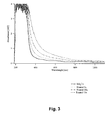
- figure 3 shows absorption spectra of TiO2 plates with different deposition treatments; and
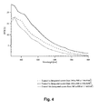
- figure 4 shows the photo current generation efficiency as a function of wavelength for Q-dot sensitized solid state heterojunction solar cells.
- Figure 1 shows the schematic build up of a solid state sensitized photovoltaic cell. From bottom to top there are :
- an ITO
transparent glass support 1; - the
glass support 1 is coated by a transparent conductinglayer 2 made of F doped SnO2, thereby the coated glass acts as a working electrode, which collects charge and current. - a dense TiO2 layer 3 for avoiding direct contact between the organic hole conductor and the SnO2, which would short circuit the cell;
- a quantum dot sensitized
nanocrystalline layer 4, forming a heterojunctio, which is build up as will be explained bellow; - the
back contact 5 of the cell is made of a fine gold layer of 10 nanometers covered by a thick nickel layer for a better current collection. - Figure 2 shows a magnified schematic view of the microscopic structure of the layered heterojunction : at the surface of TiO2 particles 6, are adsorbed Q-
dots 7; the spaces are filled withparticles 8 of an organic hole conductor. - The compact TiO2 layer is deposited on the SnO2-coated glass by spray pyrolysis. This process is performed following the procedure described in the thesis No. 2187 at EPFL of Udo Bach. The nanoporous TiO2 layer is deposited by screen printing. The plates are thereafter sintered at a temperature of 450°C for 15 min. This results in a layer with a thickness of about 2 µm. The plates are thereafter stored in water free atmosphere.
- The technique used to deposit the Q-dots follows the procedure published by Weller at al in J. Phys. Chem. 98, 1994, 3183. Two solutions are needed for this technique, the first one is a saturated Pb(NO3)2 solution in water, and the second one a 0.3M Na2S solution in water. The plates are immersed for 1 minute in the first solution. Thereafter, they are rinsed with water and dipped into the second solution for about 10 sec and then rinsed again. This deposition procedure may be repeated several times.
- After the deposition of the Q-dots, the hole-conductor is introduced into the pores of the nanocrystallinee structure by spin-coating. The spin-coating solution is a 30% by weight solution of OMeTAD in chlorobenzene. The OMeTAD may be doped with 0.2% of OMeTAD-. An amount of 150µl of spin-coating solution is used for each plate. Subsequently, the solvent is evaporated.
- A semi-transparent gold back contact is evaporated on top of the heterojunction layer under vacuum. A second contact layer made of nickel is sprayed onto the first one.
- Absorption spectra are measured with a Hewlett-Packard 8453 spectrometer and are shown in Figure 3. Figure 3 shows that repeating the Q-dot deposition treatment results in an increase of the visible absorption of the electrode. With each deposition, the optical density increases and the electrode becomes strongly coloured. The Q-dots are getting bigger with each treatment.
- Figure 4 shows the wavelength response of the photocurrent produced by the device. The incident photon to current conversion efficiency (IPCE) is plotted as a function of the wavelength of the monochromatic light. The conversion yields are high, exceeding 10 percent in the visible. This proves that the sensitization of the heterojunction by the quantum dots functions well.
- From these measurements, it can be seen that there is an optimum in the number of times the deposition treatment is repeated. For this embodiment, if only one treatment is done, there is not enough Q-dots formed on the TiO2 surface. On the other hand, if there are too many deposition treatments, typically 10, as shown in figure 4, the Q-dots get too big and the efficiency drops.
Claims (18)
- A solid state p-n heterojunction comprising an electron conductor and a hole conductor, characterised in that it further comprises a sensitising semiconductor, said sensitizing semiconductor being located at an interface between said electron conductor and said hole conductor.
- A heterojunction as claimed in claim 1, wherein said sensitizing semiconductor is in form of a coating film at the surface of said electron conductor.
- A heterojunction as claimed in claim 1, characterised in that said sensitizing semiconductor is form of particles adsorbed at the surface of said electron conductor.
- A heterojunction as claimed in claim 3, characterised in that said sensitizing semiconductor is in form of quantum-dots.
- A heterojunction as claimed in anyone of claims 1-4, characterised in that said electron conductor is an n-type semiconductor and said hole conductor is a p-type semiconductor.
- A heterojunction as claimed in claim 5, characterised in that said n-type semiconductor is a ceramic made of a finely divided large band gap metal oxide.
- A heterojunction as claimed in anyone of claims 1-6, characterised in that said electron conductor is nanocrystalline TiO2.
- A heterojunction as claimed in anyone of claims 1-7, characterised in that said hole conductor is an inorganic hole transporting solid compound.
- A heterojunction as claimed in anyone of claims 1-6, characterised in that said hole conductor is an amorphous reversibly oxydisable organic compound.
- A heterojunction as claimed in claim 9, characterised in that said organic compound is a polymer.
- A heterojunction as claimed in anyone of claims 1-7 or 9, characterised in that said hole conductor is selected from the group consisting of Spiro and Heterospirocompounds of general formula (I),wherein
 is one of C, Si, Ge or Sn, and K1 and K2 are independently one from the other conjugated systems.
- A heterojunction as claimed in claim 11, wherein said hole conductor is OMeTAD.
- A heterojunction as claimed in anyone of claims 4-12, wherein said quantum dots are particles consisting of PbS, CdS, Bi2S3, Sb2S3, Ag2S, InAs, CdTe, CdSe or HgTe or solid solutions of HgTe/CdTe or HgSe/CdSe.
- A solid state sensitized photovoltaic cell comprising a layered heterojunction as claimed in anyone of claims 1-13.
- A cell as claimed in claim 14, characterised in that it comprisesa transparent first electrode,a said layered heterojunction anda second electrode.
- A cell as claimed in claim 15, further comprising a dense semiconductive layer between said first electrode and said layered heterojunction.
- A cell as claimed in anyone of claims 14-16, characterised in that said layered heterojunction is obtained by forming quantum dots on the surface of said electron conductor by at least one deposition treatment, before providing said hole conductor to said layered heterojunction.
- A cell as claimed in claim 17, characterised in that said deposition treatment is performed 2-10 times before providing said hole conductor.
Priority Applications (6)
| Application Number | Priority Date | Filing Date | Title |
|---|---|---|---|
| EP00810681A EP1176646A1 (en) | 2000-07-28 | 2000-07-28 | Solid state heterojunction and solid state sensitized photovoltaic cell |
| AU57711/01A AU779449B2 (en) | 2000-07-28 | 2001-07-30 | Solid state heterojunction and solid state sensitized photovoltaic cell |
| US09/918,115 US6861722B2 (en) | 2000-07-28 | 2001-07-30 | Solid state heterojunction and solid state sensitized photovoltaic cell |
| JP2001230059A JP2002111031A (en) | 2000-07-28 | 2001-07-30 | Solid-state heterojunction and solid-state sensitized (photosensitive) photovoltaic cell |
| US10/885,224 US7042029B2 (en) | 2000-07-28 | 2004-07-06 | Solid state heterojunction and solid state sensitized photovoltaic cell |
| JP2013253070A JP2014042082A (en) | 2000-07-28 | 2013-12-06 | Solid hetero junction and solid sensitization (photosensitive) photovoltaic cell |
Applications Claiming Priority (1)
| Application Number | Priority Date | Filing Date | Title |
|---|---|---|---|
| EP00810681A EP1176646A1 (en) | 2000-07-28 | 2000-07-28 | Solid state heterojunction and solid state sensitized photovoltaic cell |
Publications (1)
| Publication Number | Publication Date |
|---|---|
| EP1176646A1 true EP1176646A1 (en) | 2002-01-30 |
Family
ID=8174836
Family Applications (1)
| Application Number | Title | Priority Date | Filing Date |
|---|---|---|---|
| EP00810681A Ceased EP1176646A1 (en) | 2000-07-28 | 2000-07-28 | Solid state heterojunction and solid state sensitized photovoltaic cell |
Country Status (4)
| Country | Link |
|---|---|
| US (1) | US6861722B2 (en) |
| EP (1) | EP1176646A1 (en) |
| JP (2) | JP2002111031A (en) |
| AU (1) | AU779449B2 (en) |
Cited By (66)
| Publication number | Priority date | Publication date | Assignee | Title |
|---|---|---|---|---|
| WO2004017426A1 (en) * | 2002-08-13 | 2004-02-26 | Agfa-Gevaert | Nano-porous metal oxide semiconductor spectrally sensitized with metal chalcogenide nano-particles |
| WO2004017427A1 (en) * | 2002-08-13 | 2004-02-26 | Agfa-Gevaert | Nano-porous metal oxide semiconductor spectrally sensitized with metal chalcogenide nano-particles |
| WO2004025748A1 (en) * | 2002-09-10 | 2004-03-25 | Agfa-Gevaert | Photovoltaic device comprising a 1,3,5-tris-aminophenyl-benzene compound |
| FR2862429A1 (en) * | 2003-11-17 | 2005-05-20 | Commissariat Energie Atomique | Producing semiconductor material useful in photovoltaic cells comprises grafting a porous oxide ceramic substrate with a compound that can be polymerized with a precursor of an electrically conductive polymer |
| US6929970B2 (en) | 2002-09-12 | 2005-08-16 | Agfa-Gevaert | Process for preparing nano-porous metal oxide semiconductor layers |
| EP1724838A1 (en) * | 2005-05-17 | 2006-11-22 | Ecole Polytechnique Federale De Lausanne | Tandem photovoltaic conversion device |
| WO2007065480A1 (en) * | 2005-12-09 | 2007-06-14 | Technische Universität Braunschweig | Dye sensitized solar cell |
| WO2007098378A1 (en) * | 2006-02-16 | 2007-08-30 | Solexant Corp. | Nanoparticle sensitized nanostructured solar cells |
| WO2008132455A1 (en) * | 2007-04-25 | 2008-11-06 | Nanoco Technologies Limited | Hybrid photovoltaic cells and related methods |
| WO2008098797A3 (en) * | 2007-02-16 | 2009-02-12 | Epfl Service Des Relations Ind | Semiconductor device structure |
| DE102009049696A1 (en) | 2008-10-16 | 2010-04-22 | Basf Se | New hole conductor material containing compounds useful e.g. as semiconductor material, preferably p-semiconductor in a solar cell, preferably dye photovoltaic cell, ionic liquid, solvent for chemical reaction and heat carriers |
| WO2010094636A1 (en) | 2009-02-23 | 2010-08-26 | Basf Se | Use of triarylamine derivatives as hole-conducting materials in organic solar cells and organic solar cells containing said triarylamine derivatives |
| US7800297B2 (en) | 2006-02-17 | 2010-09-21 | Solexant Corp. | Nanostructured electroluminescent device and display |
| KR100988206B1 (en) | 2008-12-12 | 2010-10-18 | 한양대학교 산학협력단 | Solar cell using carbon nanotube composite and its manufacturing method |
| WO2010142947A1 (en) | 2009-06-08 | 2010-12-16 | Isis Innovation Limited | Solid state heterojunction device |
| WO2011030117A1 (en) | 2009-09-11 | 2011-03-17 | Isis Innovation Limited | Heterojunction device |
| WO2010099858A3 (en) * | 2009-03-03 | 2011-07-21 | Karlsruher Institut Für Technologie (Kit) | Thin film solar cells |
| US7985446B2 (en) | 2004-04-30 | 2011-07-26 | Nanoco Technologies Limited | Preparation of nanoparticle materials |
| US8083971B2 (en) | 2007-07-23 | 2011-12-27 | Basf Se | Use of rylene derivatives as active components in solar cells and photodetectors |
| US8231809B2 (en) | 2005-11-10 | 2012-07-31 | Basf Aktiengesellschaft | Use of rylene derivatives as photosensitizers in solar cells |
| US8337720B2 (en) | 2008-02-25 | 2012-12-25 | Nanoco Technologies, Ltd. | Semiconductor nanoparticle capping agents |
| CN102859710A (en) * | 2010-04-06 | 2013-01-02 | 多伦多大学董事局 | Photovoltaic devices with depleted heterojunction and shell-passivated nanoparticles |
| US8394976B2 (en) | 2008-11-04 | 2013-03-12 | Nanoco Technologies, Ltd. | Surface functionalised nanoparticles |
| US8563855B2 (en) | 2007-07-23 | 2013-10-22 | Basf Se | Tandem photovoltaic cell |
| US8563348B2 (en) | 2007-04-18 | 2013-10-22 | Nanoco Technologies Ltd. | Fabrication of electrically active films based on multiple layers |
| US8597730B2 (en) | 2008-08-07 | 2013-12-03 | Nanoco Technologies Ltd. | Surface functionalised nanoparticles |
| US8741177B2 (en) | 2008-07-19 | 2014-06-03 | Nanoco Technologies Ltd. | Method for producing aqueous compatible nanoparticles |
| US8784701B2 (en) | 2007-11-30 | 2014-07-22 | Nanoco Technologies Ltd. | Preparation of nanoparticle material |
| US8816081B2 (en) | 2012-08-06 | 2014-08-26 | Basf Se | Boron containing perylene monoimides, a process for their production, their use as building blocks for the production of perylene monoimide derivatives, monoimide derivatives and their use in dye-sensitized solar cells |
| US8847197B2 (en) | 2009-09-23 | 2014-09-30 | Nanoco Technologies Ltd. | Semiconductor nanoparticle-based materials |
| US8859442B2 (en) | 2010-04-01 | 2014-10-14 | Nanoco Technologies Ltd. | Encapsulated nanoparticles |
| KR101451931B1 (en) * | 2012-12-12 | 2014-10-23 | 연세대학교 산학협력단 | Method for manufacturing colloidal quantum dot thin film and quantum dot solar cells |
| EP2560212A4 (en) * | 2010-02-18 | 2014-11-05 | Korea Res Inst Chem Tech | METHOD FOR MANUFACTURING NANOSTRUCTURED MINERAL / ORGANIC HETEROJUNCTION SOLAR CELL |
| US8921827B2 (en) | 2008-11-19 | 2014-12-30 | Nanoco Technologies, Ltd. | Semiconductor nanoparticle-based light-emitting devices and associated materials and methods |
| US8957401B2 (en) | 2009-09-23 | 2015-02-17 | Nanoco Technologies, Ltd | Semiconductor nanoparticle-based materials |
| US9001029B2 (en) | 2011-02-15 | 2015-04-07 | Basf Se | Detector for optically detecting at least one object |
| US9054325B2 (en) | 2012-02-09 | 2015-06-09 | 03;Basf Se | Rylene monoimide derivatives and use thereof as photosensitizers in solar cells and photodetectors |
| US9087991B2 (en) | 2011-02-01 | 2015-07-21 | Basf Se | Photovoltaic element |
| US9196847B2 (en) | 2005-12-23 | 2015-11-24 | Commissariat A L'energie Atomique | Sensitizing complexes, process for the preparation thereof, semiconductive inorganic/organic hybrid material comprising them, and photovoltaic cell comprising said material |
| EP3029485A1 (en) | 2011-02-15 | 2016-06-08 | Basf Se | Detector for optically detecting at least one object |
| US9385326B2 (en) | 2013-01-15 | 2016-07-05 | Basf Se | Triangulene oligomers and polymers and their use as hole conducting material |
| US9389315B2 (en) | 2012-12-19 | 2016-07-12 | Basf Se | Detector comprising a transversal optical sensor for detecting a transversal position of a light beam from an object and a longitudinal optical sensor sensing a beam cross-section of the light beam in a sensor region |
| US9428518B2 (en) | 2013-03-18 | 2016-08-30 | Basf Se | Perylenemonoimide and naphthalenemonoimide derivatives and their use in dye-sensitized solar cells |
| CN106298248A (en) * | 2016-08-31 | 2017-01-04 | 天津三安光电有限公司 | Solaode and preparation method thereof |
| US9557856B2 (en) | 2013-08-19 | 2017-01-31 | Basf Se | Optical detector |
| US9595678B2 (en) | 2010-07-23 | 2017-03-14 | Basf Se | Dye solar cell with improved stability |
| CN106637289A (en) * | 2015-10-30 | 2017-05-10 | 同济大学 | Cadmium selenide quantum dot sensitized titanium dioxide nano-rod optical electrode, and preparation and application thereof |
| US9665182B2 (en) | 2013-08-19 | 2017-05-30 | Basf Se | Detector for determining a position of at least one object |
| US9741954B2 (en) | 2013-06-13 | 2017-08-22 | Basf Se | Optical detector and method for manufacturing the same |
| US9829564B2 (en) | 2013-06-13 | 2017-11-28 | Basf Se | Detector for optically detecting at least one longitudinal coordinate of one object by determining a number of illuminated pixels |
| US10094927B2 (en) | 2014-09-29 | 2018-10-09 | Basf Se | Detector for optically determining a position of at least one object |
| US10353049B2 (en) | 2013-06-13 | 2019-07-16 | Basf Se | Detector for optically detecting an orientation of at least one object |
| US10412283B2 (en) | 2015-09-14 | 2019-09-10 | Trinamix Gmbh | Dual aperture 3D camera and method using differing aperture areas |
| US10775505B2 (en) | 2015-01-30 | 2020-09-15 | Trinamix Gmbh | Detector for an optical detection of at least one object |
| US10890491B2 (en) | 2016-10-25 | 2021-01-12 | Trinamix Gmbh | Optical detector for an optical detection |
| CN112490317A (en) * | 2020-11-27 | 2021-03-12 | 华中科技大学 | Near-infrared narrow-band detector based on cadmium selenide film and preparation method thereof |
| US10948567B2 (en) | 2016-11-17 | 2021-03-16 | Trinamix Gmbh | Detector for optically detecting at least one object |
| US10955936B2 (en) | 2015-07-17 | 2021-03-23 | Trinamix Gmbh | Detector for optically detecting at least one object |
| US11041718B2 (en) | 2014-07-08 | 2021-06-22 | Basf Se | Detector for determining a position of at least one object |
| US11060922B2 (en) | 2017-04-20 | 2021-07-13 | Trinamix Gmbh | Optical detector |
| US11067692B2 (en) | 2017-06-26 | 2021-07-20 | Trinamix Gmbh | Detector for determining a position of at least one object |
| US11125880B2 (en) | 2014-12-09 | 2021-09-21 | Basf Se | Optical detector |
| US11211513B2 (en) | 2016-07-29 | 2021-12-28 | Trinamix Gmbh | Optical sensor and detector for an optical detection |
| CN114643078A (en) * | 2022-03-29 | 2022-06-21 | 济南大学 | Preparation method of paper-based organic-inorganic double-Z-shaped heterojunction |
| US11428787B2 (en) | 2016-10-25 | 2022-08-30 | Trinamix Gmbh | Detector for an optical detection of at least one object |
| US11860292B2 (en) | 2016-11-17 | 2024-01-02 | Trinamix Gmbh | Detector and methods for authenticating at least one object |
Families Citing this family (77)
| Publication number | Priority date | Publication date | Assignee | Title |
|---|---|---|---|---|
| US6919119B2 (en) * | 2000-05-30 | 2005-07-19 | The Penn State Research Foundation | Electronic and opto-electronic devices fabricated from nanostructured high surface to volume ratio thin films |
| US7042029B2 (en) * | 2000-07-28 | 2006-05-09 | Ecole Polytechnique Federale De Lausanne (Epfl) | Solid state heterojunction and solid state sensitized photovoltaic cell |
| JP3753605B2 (en) * | 2000-11-01 | 2006-03-08 | シャープ株式会社 | Solar cell and method for manufacturing the same |
| US7777303B2 (en) * | 2002-03-19 | 2010-08-17 | The Regents Of The University Of California | Semiconductor-nanocrystal/conjugated polymer thin films |
| US7989695B2 (en) * | 2001-12-18 | 2011-08-02 | Steven Allen Carlson | Organic photovoltaic cells |
| US7594982B1 (en) | 2002-06-22 | 2009-09-29 | Nanosolar, Inc. | Nanostructured transparent conducting electrode |
| US6946597B2 (en) | 2002-06-22 | 2005-09-20 | Nanosular, Inc. | Photovoltaic devices fabricated by growth from porous template |
| US6852920B2 (en) * | 2002-06-22 | 2005-02-08 | Nanosolar, Inc. | Nano-architected/assembled solar electricity cell |
| US7253017B1 (en) | 2002-06-22 | 2007-08-07 | Nanosolar, Inc. | Molding technique for fabrication of optoelectronic devices |
| US7291782B2 (en) * | 2002-06-22 | 2007-11-06 | Nanosolar, Inc. | Optoelectronic device and fabrication method |
| KR100594578B1 (en) * | 2002-12-23 | 2006-07-03 | 삼성전자주식회사 | Light-receiving device using bonded nanoparticles |
| US7511217B1 (en) | 2003-04-19 | 2009-03-31 | Nanosolar, Inc. | Inter facial architecture for nanostructured optoelectronic devices |
| US7645934B1 (en) | 2003-04-29 | 2010-01-12 | Nanosolar, Inc. | Nanostructured layer and fabrication methods |
| US7605327B2 (en) | 2003-05-21 | 2009-10-20 | Nanosolar, Inc. | Photovoltaic devices fabricated from nanostructured template |
| US7462774B2 (en) * | 2003-05-21 | 2008-12-09 | Nanosolar, Inc. | Photovoltaic devices fabricated from insulating nanostructured template |
| CN100527445C (en) | 2003-06-12 | 2009-08-12 | 西瑞卡公司 | Steady-state non-equilibrium distribution of free carriers, photon energy upconversion and infrared imaging systems using it |
| JP2005050979A (en) * | 2003-07-31 | 2005-02-24 | Kyocera Corp | Photoelectric conversion device |
| US8304019B1 (en) | 2004-02-19 | 2012-11-06 | Nanosolar Inc. | Roll-to-roll atomic layer deposition method and system |
| US7045205B1 (en) | 2004-02-19 | 2006-05-16 | Nanosolar, Inc. | Device based on coated nanoporous structure |
| US7115304B2 (en) | 2004-02-19 | 2006-10-03 | Nanosolar, Inc. | High throughput surface treatment on coiled flexible substrates |
| WO2005114748A2 (en) * | 2004-04-13 | 2005-12-01 | Solaris Nanosciences, Inc. | Plasmon enhanced sensitized photovoltaic cells |
| US7772487B1 (en) | 2004-10-16 | 2010-08-10 | Nanosolar, Inc. | Photovoltaic cell with enhanced energy transfer |
| JP2006128204A (en) * | 2004-10-26 | 2006-05-18 | Kyocera Corp | Photoelectric conversion device and photovoltaic device using the same |
| FR2881881B1 (en) * | 2005-02-04 | 2007-06-08 | Imra Europ Sa Sa | SOLID PHOTOVOLTAIC DEVICE WITH INTERPENETRATED CONFIGURATION COMPRISING NEW ABSORBERS OR SEMICONDUCTOR MATERIALS |
| EP1819005A1 (en) | 2006-02-13 | 2007-08-15 | Ecole Polytechnique Fédérale de Lausanne (EPFL) | Ionic liquid electrolyte |
| EP1837929A1 (en) | 2006-03-23 | 2007-09-26 | Ecole Polytechnique Fédérale de Lausanne (EPFL) | Liquid Charge Transporting Material |
| WO2007112088A2 (en) * | 2006-03-24 | 2007-10-04 | Qd Vision, Inc. | Hyperspectral imaging device |
| FR2899385B1 (en) * | 2006-03-31 | 2008-06-27 | Imra Europ Sas Soc Par Actions | SOLID PHOTOVOLTAIC DEVICE COMPRISING ANTIMONY SULFIDE ABSORBER LAYER |
| US20080121271A1 (en) * | 2006-05-03 | 2008-05-29 | Rochester Institute Of Technology | Multi-junction, photovoltaic devices with nanostructured spectral enhancements and methods thereof |
| US7968792B2 (en) * | 2007-03-05 | 2011-06-28 | Seagate Technology Llc | Quantum dot sensitized wide bandgap semiconductor photovoltaic devices & methods of fabricating same |
| KR100934732B1 (en) * | 2007-06-01 | 2009-12-30 | 한국기계연구원 | Solar cell using quantum dots and manufacturing method thereof |
| US20110174364A1 (en) * | 2007-06-26 | 2011-07-21 | Honeywell International Inc. | nanostructured solar cell |
| WO2009002551A1 (en) * | 2007-06-26 | 2008-12-31 | Qd Vision, Inc. | Photovoltaic devices including quantum dot down-conversion materials useful for solar cells and materials including quantum dots |
| US20110139233A1 (en) * | 2009-12-11 | 2011-06-16 | Honeywell International Inc. | Quantum dot solar cell |
| US20100043874A1 (en) * | 2007-06-26 | 2010-02-25 | Honeywell International Inc. | Nanostructured solar cell |
| US8710354B2 (en) * | 2007-12-19 | 2014-04-29 | Honeywell International Inc. | Solar cell with hyperpolarizable absorber |
| US8288649B2 (en) * | 2008-02-26 | 2012-10-16 | Honeywell International Inc. | Quantum dot solar cell |
| US20090217967A1 (en) * | 2008-02-29 | 2009-09-03 | International Business Machines Corporation | Porous silicon quantum dot photodetector |
| US8299355B2 (en) * | 2008-04-22 | 2012-10-30 | Honeywell International Inc. | Quantum dot solar cell |
| US8373063B2 (en) * | 2008-04-22 | 2013-02-12 | Honeywell International Inc. | Quantum dot solar cell |
| US20100006148A1 (en) * | 2008-07-08 | 2010-01-14 | Honeywell International Inc. | Solar cell with porous insulating layer |
| US20100012168A1 (en) * | 2008-07-18 | 2010-01-21 | Honeywell International | Quantum dot solar cell |
| US8455757B2 (en) | 2008-08-20 | 2013-06-04 | Honeywell International Inc. | Solar cell with electron inhibiting layer |
| US8927852B2 (en) * | 2008-08-21 | 2015-01-06 | Seagate Technology Llc | Photovoltaic device with an up-converting quantum dot layer and absorber |
| WO2010055505A1 (en) * | 2008-11-12 | 2010-05-20 | D.C. Sirica Ltd. | Production of amorphous and crystalline silicon |
| KR101060229B1 (en) | 2008-12-12 | 2011-08-29 | 포항공과대학교 산학협력단 | Photoelectric conversion device using quantum dot dendrimer |
| US8227687B2 (en) * | 2009-02-04 | 2012-07-24 | Honeywell International Inc. | Quantum dot solar cell |
| US8227686B2 (en) * | 2009-02-04 | 2012-07-24 | Honeywell International Inc. | Quantum dot solar cell |
| JP2009182333A (en) * | 2009-02-05 | 2009-08-13 | Sony Corp | Electronic device and manufacturing method thereof |
| US20100258163A1 (en) * | 2009-04-14 | 2010-10-14 | Honeywell International Inc. | Thin-film photovoltaics |
| TWI475701B (en) * | 2009-05-05 | 2015-03-01 | Eternal Materials Co Ltd | Dye-sensitized solar cell using composite semiconductor material |
| US8426728B2 (en) * | 2009-06-12 | 2013-04-23 | Honeywell International Inc. | Quantum dot solar cells |
| US20100326499A1 (en) * | 2009-06-30 | 2010-12-30 | Honeywell International Inc. | Solar cell with enhanced efficiency |
| US20110108102A1 (en) * | 2009-11-06 | 2011-05-12 | Honeywell International Inc. | Solar cell with enhanced efficiency |
| US8372678B2 (en) * | 2009-12-21 | 2013-02-12 | Honeywell International Inc. | Counter electrode for solar cell |
| US20110155233A1 (en) * | 2009-12-29 | 2011-06-30 | Honeywell International Inc. | Hybrid solar cells |
| TWI394309B (en) * | 2009-12-30 | 2013-04-21 | Ind Tech Res Inst | Dye sensitized solar cell |
| CN102712659B (en) | 2010-01-18 | 2015-09-30 | 默克专利有限公司 | Ionogen preparaton |
| AU2011206738A1 (en) | 2010-01-18 | 2012-09-06 | Merck Patent Gmbh | Compounds containing perfluoroalkyl-cyano-alkoxy-borate anions or perfluoroalkyl-cyano-alkoxy-fluoro-borate anions |
| TW201132629A (en) | 2010-01-18 | 2011-10-01 | Merck Patent Gmbh | Electrolyte formulations |
| WO2011102673A2 (en) * | 2010-02-18 | 2011-08-25 | 한국화학연구원 | All-solid-state heterojunction solar cell |
| GB201004106D0 (en) * | 2010-03-11 | 2010-04-28 | Isis Innovation | Device |
| EP2388853A1 (en) | 2010-05-20 | 2011-11-23 | Fundacion Cidetec | Ionic liquid based electrolytes containing sulfide/polysulfide redox couple and uses thereof |
| JP5852656B2 (en) | 2010-09-27 | 2016-02-03 | メルク パテント ゲゼルシャフト ミット ベシュレンクテル ハフツングMerck Patent Gesellschaft mit beschraenkter Haftung | Functionalized fluoroalkyl fluorophosphate |
| CN103140905B (en) | 2010-09-30 | 2016-09-28 | 默克专利有限公司 | Electrolyte preparaton |
| JP5805394B2 (en) * | 2011-01-04 | 2015-11-04 | 公立大学法人 滋賀県立大学 | Manufacturing method of organic thin film solar cell |
| CN103687863B9 (en) | 2011-07-15 | 2016-07-27 | 默克专利有限公司 | Compound containing alkyl-cyano group-borate or alkyl-cyano group-fluoboric acid root anion |
| JP5985626B2 (en) | 2011-07-15 | 2016-09-06 | メルク パテント ゲゼルシャフト ミット ベシュレンクテル ハフツングMerck Patent Gesellschaft mit beschraenkter Haftung | Compounds containing alkyl-alkoxy-cyano-borate anions |
| JP2013089368A (en) * | 2011-10-14 | 2013-05-13 | Ulvac Japan Ltd | Quantum dot sensitization type solar cell |
| JP5891005B2 (en) * | 2011-10-31 | 2016-03-22 | 積水化学工業株式会社 | Organic inorganic composite thin film solar cell |
| JP5845059B2 (en) * | 2011-10-31 | 2016-01-20 | 積水化学工業株式会社 | Organic inorganic composite thin film solar cell |
| CN102941077A (en) * | 2012-11-07 | 2013-02-27 | 复旦大学 | Preparation method of titanium dioxide nanotube thin film with visible-light activity |
| JP6251742B2 (en) * | 2012-12-04 | 2017-12-20 | シャープ株式会社 | Quantum dot sensitized solar cell |
| EP2883881A1 (en) | 2013-12-12 | 2015-06-17 | Merck Patent GmbH | Cobaltcomplex salts and mixtures of Cobaltcomplex salts for use in DSSC |
| DE102013021029A1 (en) | 2013-12-17 | 2015-07-02 | Julius-Maximilians-Universität Würzburg | Cobalt complex salts |
| KR102712138B1 (en) | 2018-06-14 | 2024-09-27 | 삼성전자주식회사 | Quantum dots and production method thereof |
| US11581501B2 (en) * | 2018-06-20 | 2023-02-14 | Samsung Electronics Co., Ltd. | Electronic device and production method thereof |
Citations (2)
| Publication number | Priority date | Publication date | Assignee | Title |
|---|---|---|---|---|
| FR2694451A1 (en) * | 1992-07-29 | 1994-02-04 | Asulab Sa | Photovoltaic cell. |
| DE19711713A1 (en) * | 1997-03-20 | 1998-10-01 | Hoechst Ag | Photovoltaic cell |
Family Cites Families (5)
| Publication number | Priority date | Publication date | Assignee | Title |
|---|---|---|---|---|
| DE4207659A1 (en) * | 1992-03-11 | 1993-09-16 | Abb Patent Gmbh | METHOD FOR PRODUCING A PHOTOELECTROCHEMICAL CELL AND A CLEARLY PRODUCED CELL |
| DE19533850A1 (en) * | 1995-09-13 | 1997-03-27 | Hoechst Ag | Photovoltaic cell |
| US5728801A (en) * | 1996-08-13 | 1998-03-17 | The Dow Chemical Company | Poly (arylamines) and films thereof |
| JP2000106224A (en) * | 1998-09-29 | 2000-04-11 | Fuji Photo Film Co Ltd | Photoelectric conversion element and photo electrochemical cell |
| ATE402478T1 (en) * | 1998-09-30 | 2008-08-15 | Fujifilm Corp | SEMICONDUCTOR PARTICLES SENSITIZED WITH A METHINE DYE |
-
2000
- 2000-07-28 EP EP00810681A patent/EP1176646A1/en not_active Ceased
-
2001
- 2001-07-30 AU AU57711/01A patent/AU779449B2/en not_active Expired
- 2001-07-30 JP JP2001230059A patent/JP2002111031A/en not_active Withdrawn
- 2001-07-30 US US09/918,115 patent/US6861722B2/en not_active Expired - Lifetime
-
2013
- 2013-12-06 JP JP2013253070A patent/JP2014042082A/en active Pending
Patent Citations (2)
| Publication number | Priority date | Publication date | Assignee | Title |
|---|---|---|---|---|
| FR2694451A1 (en) * | 1992-07-29 | 1994-02-04 | Asulab Sa | Photovoltaic cell. |
| DE19711713A1 (en) * | 1997-03-20 | 1998-10-01 | Hoechst Ag | Photovoltaic cell |
Non-Patent Citations (8)
| Title |
|---|
| BACH U ET AL: "SOLID-STATE DYE-SENSITIZED MESOPOROUS TIO2 SOLAR CELLS WITH HIGH PHOTON-TO-ELECTRON CONVERSION EFFICIENCIES", NATURE,GB,MACMILLAN JOURNALS LTD. LONDON, vol. 395, 8 October 1998 (1998-10-08), pages 583 - 585, XP000783901, ISSN: 0028-0836 * |
| C ROST ET AL: "Transparent p-type semiconductors for the ETA solar cell with Extremely Thin Absorber", 2ND WORLD CONFERENCE AND EXHIBITION ON PHOTOVOLTAIC SOLAR ENERGY CONVERSION, 6 July 1998 (1998-07-06) - 10 July 1998 (1998-07-10), VIENNA, AT, pages 212 - 215, XP002141360 * |
| GREENHAM N C ET AL: "CHARGE SEPARATION AND TRANSPORT IN CONJUGATED-POLYMER/SEMICONDUCTOR-N ANOCRYSTAL COMPOSITES STUDIED BY PHOTOLUMINESCENCE QUENCHING AND PHOTOCONDUCTIVITY", PHYSICAL REVIEW, B. CONDENSED MATTER,US,AMERICAN INSTITUTE OF PHYSICS. NEW YORK, vol. 54, no. 24, 15 December 1996 (1996-12-15), pages 17628 - 17637, XP002060964, ISSN: 0163-1829 * |
| MOELLER J ET AL: "A NOVEL DEPOSITION TECHNIQUE FOR COMPOUND SEMICONDUCTORS ON HIGHLY POROUS SUBSTRATES: ILGAR", THIN SOLID FILMS,ELSEVIER-SEQUOIA S.A. LAUSANNE,CH, vol. 361/362, 21 February 2000 (2000-02-21), pages 113 - 117, XP000922979, ISSN: 0040-6090 * |
| S. SIEBENTRITT ET AL.: "CdTe and CdS as extremely thin absorber materials in an eta solar cell", 14TH EUROPEAN PHOTOVOLTAIC SOLAR ENERGY CONFERENCE, 30 June 1997 (1997-06-30) - 4 July 1997 (1997-07-04), BARCELONA, ES, pages 1823 - 1826, XP002156223 * |
| SALAFSKY J S ET AL: "PHOTOINDUCED CHARGE SEPARATION AND RECOMBINATION IN A CONJUGATED POLYMER-SEMICONDUCTOR NANOCRYSTAL COMPOSITE", CHEMICAL PHYSICS LETTERS,AMSTERDAM,NL, vol. 290, no. 4/06, 3 July 1998 (1998-07-03), pages 297 - 303, XP000884003 * |
| VOGEL R ET AL: "QUANTUM-SIZED PBS, CDS, AG2S, AND BI2S3 PARTICLES AS SENSITIZERS FOR VARIOUS NANOPOROUS WIDE-BANDGAP SEMICONDUCTORS", JOURNAL OF PHYSICAL CHEMISTRY,AMERICAN CHEMICAL SOCIETY,US, vol. 98, no. 12, 1994, pages 3183 - 3188, XP000956096, ISSN: 0022-3654 * |
| VOGEL R ET AL: "SENSITIZATION OF HIGHLY POROUS, POLYCRYSTALLINE TIO2 ELECTRODES BY QUANTUM SIZED CDS", CHEMICAL PHYSICS LETTERS,AMSTERDAM,NL, vol. 174, no. 3/04, 9 November 1990 (1990-11-09), pages 241 - 246, XP000956095 * |
Cited By (94)
| Publication number | Priority date | Publication date | Assignee | Title |
|---|---|---|---|---|
| WO2004017426A1 (en) * | 2002-08-13 | 2004-02-26 | Agfa-Gevaert | Nano-porous metal oxide semiconductor spectrally sensitized with metal chalcogenide nano-particles |
| WO2004017427A1 (en) * | 2002-08-13 | 2004-02-26 | Agfa-Gevaert | Nano-porous metal oxide semiconductor spectrally sensitized with metal chalcogenide nano-particles |
| WO2004025748A1 (en) * | 2002-09-10 | 2004-03-25 | Agfa-Gevaert | Photovoltaic device comprising a 1,3,5-tris-aminophenyl-benzene compound |
| US6929970B2 (en) | 2002-09-12 | 2005-08-16 | Agfa-Gevaert | Process for preparing nano-porous metal oxide semiconductor layers |
| FR2862429A1 (en) * | 2003-11-17 | 2005-05-20 | Commissariat Energie Atomique | Producing semiconductor material useful in photovoltaic cells comprises grafting a porous oxide ceramic substrate with a compound that can be polymerized with a precursor of an electrically conductive polymer |
| WO2005050752A1 (en) * | 2003-11-17 | 2005-06-02 | Commissariat A L'energie Atomique | Inorganic/organic semiconductor p-n hybrid material, production method thereof and photovoltaic cell comprising same |
| US8524365B2 (en) | 2004-04-30 | 2013-09-03 | Nanoco Technologies Ltd. | Preparation of nanoparticle materials |
| US7985446B2 (en) | 2004-04-30 | 2011-07-26 | Nanoco Technologies Limited | Preparation of nanoparticle materials |
| US8062703B2 (en) | 2004-04-30 | 2011-11-22 | Nanoco Technologies Ltd. | Preparation of nanoparticle materials |
| EP1724838A1 (en) * | 2005-05-17 | 2006-11-22 | Ecole Polytechnique Federale De Lausanne | Tandem photovoltaic conversion device |
| US8501046B2 (en) | 2005-11-10 | 2013-08-06 | Basf Se | Use of rylene derivatives as photosensitizers in solar cells |
| US8231809B2 (en) | 2005-11-10 | 2012-07-31 | Basf Aktiengesellschaft | Use of rylene derivatives as photosensitizers in solar cells |
| WO2007065480A1 (en) * | 2005-12-09 | 2007-06-14 | Technische Universität Braunschweig | Dye sensitized solar cell |
| US9196847B2 (en) | 2005-12-23 | 2015-11-24 | Commissariat A L'energie Atomique | Sensitizing complexes, process for the preparation thereof, semiconductive inorganic/organic hybrid material comprising them, and photovoltaic cell comprising said material |
| WO2007098378A1 (en) * | 2006-02-16 | 2007-08-30 | Solexant Corp. | Nanoparticle sensitized nanostructured solar cells |
| US7800297B2 (en) | 2006-02-17 | 2010-09-21 | Solexant Corp. | Nanostructured electroluminescent device and display |
| WO2008098797A3 (en) * | 2007-02-16 | 2009-02-12 | Epfl Service Des Relations Ind | Semiconductor device structure |
| US8563348B2 (en) | 2007-04-18 | 2013-10-22 | Nanoco Technologies Ltd. | Fabrication of electrically active films based on multiple layers |
| CN101689609B (en) * | 2007-04-25 | 2012-05-30 | 纳米技术有限公司 | Hybrid photovoltaic cells and related methods |
| US8394663B2 (en) | 2007-04-25 | 2013-03-12 | Nanoco Technologies, Ltd. | Hybrid photovoltaic cells and related methods |
| WO2008132455A1 (en) * | 2007-04-25 | 2008-11-06 | Nanoco Technologies Limited | Hybrid photovoltaic cells and related methods |
| US8563855B2 (en) | 2007-07-23 | 2013-10-22 | Basf Se | Tandem photovoltaic cell |
| US8083971B2 (en) | 2007-07-23 | 2011-12-27 | Basf Se | Use of rylene derivatives as active components in solar cells and photodetectors |
| US9251922B2 (en) | 2007-11-30 | 2016-02-02 | Nanoco Technologies, Ltd. | Preparation of nanoparticle material |
| US8784701B2 (en) | 2007-11-30 | 2014-07-22 | Nanoco Technologies Ltd. | Preparation of nanoparticle material |
| US8337720B2 (en) | 2008-02-25 | 2012-12-25 | Nanoco Technologies, Ltd. | Semiconductor nanoparticle capping agents |
| US8741177B2 (en) | 2008-07-19 | 2014-06-03 | Nanoco Technologies Ltd. | Method for producing aqueous compatible nanoparticles |
| US8597730B2 (en) | 2008-08-07 | 2013-12-03 | Nanoco Technologies Ltd. | Surface functionalised nanoparticles |
| DE102009049696A1 (en) | 2008-10-16 | 2010-04-22 | Basf Se | New hole conductor material containing compounds useful e.g. as semiconductor material, preferably p-semiconductor in a solar cell, preferably dye photovoltaic cell, ionic liquid, solvent for chemical reaction and heat carriers |
| US8394976B2 (en) | 2008-11-04 | 2013-03-12 | Nanoco Technologies, Ltd. | Surface functionalised nanoparticles |
| US8921827B2 (en) | 2008-11-19 | 2014-12-30 | Nanoco Technologies, Ltd. | Semiconductor nanoparticle-based light-emitting devices and associated materials and methods |
| KR100988206B1 (en) | 2008-12-12 | 2010-10-18 | 한양대학교 산학협력단 | Solar cell using carbon nanotube composite and its manufacturing method |
| WO2010094636A1 (en) | 2009-02-23 | 2010-08-26 | Basf Se | Use of triarylamine derivatives as hole-conducting materials in organic solar cells and organic solar cells containing said triarylamine derivatives |
| WO2010099858A3 (en) * | 2009-03-03 | 2011-07-21 | Karlsruher Institut Für Technologie (Kit) | Thin film solar cells |
| WO2010142947A1 (en) | 2009-06-08 | 2010-12-16 | Isis Innovation Limited | Solid state heterojunction device |
| US9349971B2 (en) | 2009-06-08 | 2016-05-24 | Isis Innovation Limited | Solid state heterojunction device |
| WO2011030117A1 (en) | 2009-09-11 | 2011-03-17 | Isis Innovation Limited | Heterojunction device |
| US9543481B2 (en) | 2009-09-23 | 2017-01-10 | Nanoco Technologies Ltd. | Semiconductor nanoparticle-based materials |
| US8847197B2 (en) | 2009-09-23 | 2014-09-30 | Nanoco Technologies Ltd. | Semiconductor nanoparticle-based materials |
| US8957401B2 (en) | 2009-09-23 | 2015-02-17 | Nanoco Technologies, Ltd | Semiconductor nanoparticle-based materials |
| EP2560212A4 (en) * | 2010-02-18 | 2014-11-05 | Korea Res Inst Chem Tech | METHOD FOR MANUFACTURING NANOSTRUCTURED MINERAL / ORGANIC HETEROJUNCTION SOLAR CELL |
| US9059418B2 (en) | 2010-02-18 | 2015-06-16 | Korea Research Institute Of Chemical Technology | Method for manufacturing a nanostructured inorganic/organic heterojunction solar cell |
| US9159590B2 (en) | 2010-04-01 | 2015-10-13 | Nanoco Technologies, Ltd. | Encapsulated nanoparticles |
| US8859442B2 (en) | 2010-04-01 | 2014-10-14 | Nanoco Technologies Ltd. | Encapsulated nanoparticles |
| US10784388B2 (en) | 2010-04-06 | 2020-09-22 | The Governing Council Of The University Of Toronto | Photovoltaic devices with depleted heterojunctions and shell-passivated nanoparticles |
| CN102859710B (en) * | 2010-04-06 | 2016-10-19 | 多伦多大学董事局 | Optoelectronic devices, nanoparticles, and methods of forming nanoparticles |
| CN106167704B (en) * | 2010-04-06 | 2020-09-04 | 多伦多大学董事局 | Optoelectronic devices, nanoparticles, and methods of forming nanoparticles |
| CN102859710A (en) * | 2010-04-06 | 2013-01-02 | 多伦多大学董事局 | Photovoltaic devices with depleted heterojunction and shell-passivated nanoparticles |
| CN106167704A (en) * | 2010-04-06 | 2016-11-30 | 多伦多大学董事局 | Electrooptical device, nano-particle and the method forming nano-particle |
| US9595678B2 (en) | 2010-07-23 | 2017-03-14 | Basf Se | Dye solar cell with improved stability |
| US9087991B2 (en) | 2011-02-01 | 2015-07-21 | Basf Se | Photovoltaic element |
| EP3029485A1 (en) | 2011-02-15 | 2016-06-08 | Basf Se | Detector for optically detecting at least one object |
| US9001029B2 (en) | 2011-02-15 | 2015-04-07 | Basf Se | Detector for optically detecting at least one object |
| US9054325B2 (en) | 2012-02-09 | 2015-06-09 | 03;Basf Se | Rylene monoimide derivatives and use thereof as photosensitizers in solar cells and photodetectors |
| US9105410B2 (en) | 2012-08-06 | 2015-08-11 | Basf Se | Boron containing perylene monoimides, a process for their production, their use as building blocks for the production of perylene monoimide derivatives, monoimide derivatives and their use in dye-sensitized solar cells |
| US9624375B2 (en) | 2012-08-06 | 2017-04-18 | Basf Se | Boron containing perylene monoimides, a process for their production, their use as building blocks for the production of perylene monoimide derivatives, monoimide derivatives and their use in dye-sensitized solar cells |
| US8816081B2 (en) | 2012-08-06 | 2014-08-26 | Basf Se | Boron containing perylene monoimides, a process for their production, their use as building blocks for the production of perylene monoimide derivatives, monoimide derivatives and their use in dye-sensitized solar cells |
| KR101451931B1 (en) * | 2012-12-12 | 2014-10-23 | 연세대학교 산학협력단 | Method for manufacturing colloidal quantum dot thin film and quantum dot solar cells |
| US9389315B2 (en) | 2012-12-19 | 2016-07-12 | Basf Se | Detector comprising a transversal optical sensor for detecting a transversal position of a light beam from an object and a longitudinal optical sensor sensing a beam cross-section of the light beam in a sensor region |
| US10120078B2 (en) | 2012-12-19 | 2018-11-06 | Basf Se | Detector having a transversal optical sensor and a longitudinal optical sensor |
| US9385326B2 (en) | 2013-01-15 | 2016-07-05 | Basf Se | Triangulene oligomers and polymers and their use as hole conducting material |
| US9428518B2 (en) | 2013-03-18 | 2016-08-30 | Basf Se | Perylenemonoimide and naphthalenemonoimide derivatives and their use in dye-sensitized solar cells |
| US10845459B2 (en) | 2013-06-13 | 2020-11-24 | Basf Se | Detector for optically detecting at least one object |
| US9741954B2 (en) | 2013-06-13 | 2017-08-22 | Basf Se | Optical detector and method for manufacturing the same |
| US9829564B2 (en) | 2013-06-13 | 2017-11-28 | Basf Se | Detector for optically detecting at least one longitudinal coordinate of one object by determining a number of illuminated pixels |
| US10353049B2 (en) | 2013-06-13 | 2019-07-16 | Basf Se | Detector for optically detecting an orientation of at least one object |
| US9989623B2 (en) | 2013-06-13 | 2018-06-05 | Basf Se | Detector for determining a longitudinal coordinate of an object via an intensity distribution of illuminated pixels |
| US10823818B2 (en) | 2013-06-13 | 2020-11-03 | Basf Se | Detector for optically detecting at least one object |
| US10012532B2 (en) | 2013-08-19 | 2018-07-03 | Basf Se | Optical detector |
| US9958535B2 (en) | 2013-08-19 | 2018-05-01 | Basf Se | Detector for determining a position of at least one object |
| US9665182B2 (en) | 2013-08-19 | 2017-05-30 | Basf Se | Detector for determining a position of at least one object |
| US9557856B2 (en) | 2013-08-19 | 2017-01-31 | Basf Se | Optical detector |
| US11041718B2 (en) | 2014-07-08 | 2021-06-22 | Basf Se | Detector for determining a position of at least one object |
| US10094927B2 (en) | 2014-09-29 | 2018-10-09 | Basf Se | Detector for optically determining a position of at least one object |
| US11125880B2 (en) | 2014-12-09 | 2021-09-21 | Basf Se | Optical detector |
| US10775505B2 (en) | 2015-01-30 | 2020-09-15 | Trinamix Gmbh | Detector for an optical detection of at least one object |
| US10955936B2 (en) | 2015-07-17 | 2021-03-23 | Trinamix Gmbh | Detector for optically detecting at least one object |
| US10412283B2 (en) | 2015-09-14 | 2019-09-10 | Trinamix Gmbh | Dual aperture 3D camera and method using differing aperture areas |
| CN106637289A (en) * | 2015-10-30 | 2017-05-10 | 同济大学 | Cadmium selenide quantum dot sensitized titanium dioxide nano-rod optical electrode, and preparation and application thereof |
| CN106637289B (en) * | 2015-10-30 | 2019-01-25 | 同济大学 | Cadmium Selenide Quantum Dot Sensitized Titanium Dioxide Nanorod Photoelectrode and Its Preparation and Application |
| US11211513B2 (en) | 2016-07-29 | 2021-12-28 | Trinamix Gmbh | Optical sensor and detector for an optical detection |
| CN106298248A (en) * | 2016-08-31 | 2017-01-04 | 天津三安光电有限公司 | Solaode and preparation method thereof |
| US10890491B2 (en) | 2016-10-25 | 2021-01-12 | Trinamix Gmbh | Optical detector for an optical detection |
| US11428787B2 (en) | 2016-10-25 | 2022-08-30 | Trinamix Gmbh | Detector for an optical detection of at least one object |
| US10948567B2 (en) | 2016-11-17 | 2021-03-16 | Trinamix Gmbh | Detector for optically detecting at least one object |
| US11415661B2 (en) | 2016-11-17 | 2022-08-16 | Trinamix Gmbh | Detector for optically detecting at least one object |
| US11635486B2 (en) | 2016-11-17 | 2023-04-25 | Trinamix Gmbh | Detector for optically detecting at least one object |
| US11698435B2 (en) | 2016-11-17 | 2023-07-11 | Trinamix Gmbh | Detector for optically detecting at least one object |
| US11860292B2 (en) | 2016-11-17 | 2024-01-02 | Trinamix Gmbh | Detector and methods for authenticating at least one object |
| US11060922B2 (en) | 2017-04-20 | 2021-07-13 | Trinamix Gmbh | Optical detector |
| US11067692B2 (en) | 2017-06-26 | 2021-07-20 | Trinamix Gmbh | Detector for determining a position of at least one object |
| CN112490317A (en) * | 2020-11-27 | 2021-03-12 | 华中科技大学 | Near-infrared narrow-band detector based on cadmium selenide film and preparation method thereof |
| CN114643078A (en) * | 2022-03-29 | 2022-06-21 | 济南大学 | Preparation method of paper-based organic-inorganic double-Z-shaped heterojunction |
| CN114643078B (en) * | 2022-03-29 | 2023-08-25 | 济南大学 | A preparation method of paper-based organic-inorganic double Z-type heterojunction |
Also Published As
| Publication number | Publication date |
|---|---|
| JP2002111031A (en) | 2002-04-12 |
| JP2014042082A (en) | 2014-03-06 |
| AU779449B2 (en) | 2005-01-27 |
| US6861722B2 (en) | 2005-03-01 |
| US20020017656A1 (en) | 2002-02-14 |
| AU5771101A (en) | 2002-01-31 |
Similar Documents
| Publication | Publication Date | Title |
|---|---|---|
| US6861722B2 (en) | Solid state heterojunction and solid state sensitized photovoltaic cell | |
| US7042029B2 (en) | Solid state heterojunction and solid state sensitized photovoltaic cell | |
| US20210313120A1 (en) | MXene-Modified Hybrid Photoconverter | |
| US8426722B2 (en) | Semiconductor grain and oxide layer for photovoltaic cells | |
| US8373060B2 (en) | Semiconductor grain microstructures for photovoltaic cells | |
| Yonehara et al. | Photoelectrical properties of double-layer organic solar cells using C60 and phthalocyanines | |
| US6929970B2 (en) | Process for preparing nano-porous metal oxide semiconductor layers | |
| US8158880B1 (en) | Thin-film photovoltaic structures including semiconductor grain and oxide layers | |
| US20070012356A1 (en) | Process for the production of thin layers, preferably for a photovoltaic cell | |
| WO2019048839A1 (en) | Multi-junction photovoltaic device | |
| WO2014036179A2 (en) | Copper oxide core/shell nanocrystals for use in photovoltaic cells | |
| Jiang et al. | Engineering the interfaces of ITO@ Cu2S nanowire arrays toward efficient and stable counter electrodes for quantum-dot-sensitized solar cells | |
| JP4299960B2 (en) | Photoelectric conversion element and solar cell | |
| EP1107332A2 (en) | Photoelectric conversion device | |
| JP4392769B2 (en) | Photoelectric conversion element, solar cell and solar cell module | |
| JP2001156314A (en) | Photoelectric conversion element and solar cell | |
| US20130042906A1 (en) | Quantum-dot sensitized solar cell | |
| JP2001185743A (en) | Photoelectric conversion element and solar cell | |
| EP4084104A1 (en) | Solar cell | |
| Deshpande et al. | Review of hybrid solar cells based on CdSe and TiO2 materials | |
| KR102081789B1 (en) | Quantumdot solar cell including adsorbant | |
| WO2004025748A1 (en) | Photovoltaic device comprising a 1,3,5-tris-aminophenyl-benzene compound | |
| JP5194364B2 (en) | Penetration solid-state photovoltaic device containing novel absorber or semiconductor material | |
| EP4177977A1 (en) | Solar cell and photoelectric conversion element | |
| JP2001257370A (en) | Photoelectric conversion element and photocell |
Legal Events
| Date | Code | Title | Description |
|---|---|---|---|
| PUAI | Public reference made under article 153(3) epc to a published international application that has entered the european phase |
Free format text: ORIGINAL CODE: 0009012 |
|
| AK | Designated contracting states |
Kind code of ref document: A1 Designated state(s): AT BE CH CY DE DK ES FI FR GB GR IE IT LI LU MC NL PT SE |
|
| AX | Request for extension of the european patent |
Free format text: AL;LT;LV;MK;RO;SI |
|
| 17P | Request for examination filed |
Effective date: 20020603 |
|
| AKX | Designation fees paid |
Free format text: AT BE CH CY DE DK ES FI FR GB GR IE IT LI LU MC NL PT SE |
|
| RAP1 | Party data changed (applicant data changed or rights of an application transferred) |
Owner name: ECOLE POLYTECHNIQUE FEDERALE DE LAUSANNE (EPFL) |
|
| STAA | Information on the status of an ep patent application or granted ep patent |
Free format text: STATUS: THE APPLICATION HAS BEEN REFUSED |
|
| 18R | Application refused |
Effective date: 20140709 |
|
| REG | Reference to a national code |
Ref country code: DE Ref legal event code: R079 Free format text: PREVIOUS MAIN CLASS: H01L0051200000 Ipc: H01L0051050000 |
|
| REG | Reference to a national code |
Ref country code: DE Ref legal event code: R079 Free format text: PREVIOUS MAIN CLASS: H01L0051200000 Ipc: H01L0051050000 Effective date: 20150213 |