EP1180494A2 - Thin film resonators fabricated on membranes created by front side releasing - Google Patents
Thin film resonators fabricated on membranes created by front side releasing Download PDFInfo
- Publication number
- EP1180494A2 EP1180494A2 EP01306284A EP01306284A EP1180494A2 EP 1180494 A2 EP1180494 A2 EP 1180494A2 EP 01306284 A EP01306284 A EP 01306284A EP 01306284 A EP01306284 A EP 01306284A EP 1180494 A2 EP1180494 A2 EP 1180494A2
- Authority
- EP
- European Patent Office
- Prior art keywords
- resonator
- electrode
- wafer
- layer
- piezoelectric
- Prior art date
- Legal status (The legal status is an assumption and is not a legal conclusion. Google has not performed a legal analysis and makes no representation as to the accuracy of the status listed.)
- Granted
Links
Images

Classifications
-
- H—ELECTRICITY
- H03—ELECTRONIC CIRCUITRY
- H03H—IMPEDANCE NETWORKS, e.g. RESONANT CIRCUITS; RESONATORS
- H03H9/00—Networks comprising electromechanical or electro-acoustic elements; Electromechanical resonators
- H03H9/15—Constructional features of resonators consisting of piezoelectric or electrostrictive material
- H03H9/17—Constructional features of resonators consisting of piezoelectric or electrostrictive material having a single resonator
- H03H9/171—Constructional features of resonators consisting of piezoelectric or electrostrictive material having a single resonator implemented with thin-film techniques, i.e. of the film bulk acoustic resonator [FBAR] type
- H03H9/172—Means for mounting on a substrate, i.e. means constituting the material interface confining the waves to a volume
- H03H9/173—Air-gaps
-
- B—PERFORMING OPERATIONS; TRANSPORTING
- B81—MICROSTRUCTURAL TECHNOLOGY
- B81C—PROCESSES OR APPARATUS SPECIALLY ADAPTED FOR THE MANUFACTURE OR TREATMENT OF MICROSTRUCTURAL DEVICES OR SYSTEMS
- B81C1/00—Manufacture or treatment of devices or systems in or on a substrate
- B81C1/00015—Manufacture or treatment of devices or systems in or on a substrate for manufacturing microsystems
- B81C1/00134—Manufacture or treatment of devices or systems in or on a substrate for manufacturing microsystems comprising flexible or deformable structures
- B81C1/00142—Bridges
-
- H—ELECTRICITY
- H03—ELECTRONIC CIRCUITRY
- H03H—IMPEDANCE NETWORKS, e.g. RESONANT CIRCUITS; RESONATORS
- H03H3/00—Apparatus or processes specially adapted for the manufacture of impedance networks, resonating circuits, resonators
- H03H3/007—Apparatus or processes specially adapted for the manufacture of impedance networks, resonating circuits, resonators for the manufacture of electromechanical resonators or networks
- H03H3/02—Apparatus or processes specially adapted for the manufacture of impedance networks, resonating circuits, resonators for the manufacture of electromechanical resonators or networks for the manufacture of piezoelectric or electrostrictive resonators or networks
-
- B—PERFORMING OPERATIONS; TRANSPORTING
- B81—MICROSTRUCTURAL TECHNOLOGY
- B81B—MICROSTRUCTURAL DEVICES OR SYSTEMS, e.g. MICROMECHANICAL DEVICES
- B81B2201/00—Specific applications of microelectromechanical systems
- B81B2201/02—Sensors
- B81B2201/0271—Resonators; ultrasonic resonators
-
- B—PERFORMING OPERATIONS; TRANSPORTING
- B81—MICROSTRUCTURAL TECHNOLOGY
- B81C—PROCESSES OR APPARATUS SPECIALLY ADAPTED FOR THE MANUFACTURE OR TREATMENT OF MICROSTRUCTURAL DEVICES OR SYSTEMS
- B81C2201/00—Manufacture or treatment of microstructural devices or systems
- B81C2201/01—Manufacture or treatment of microstructural devices or systems in or on a substrate
- B81C2201/0101—Shaping material; Structuring the bulk substrate or layers on the substrate; Film patterning
- B81C2201/0128—Processes for removing material
- B81C2201/013—Etching
- B81C2201/0135—Controlling etch progression
- B81C2201/014—Controlling etch progression by depositing an etch stop layer, e.g. silicon nitride, silicon oxide, metal
-
- H—ELECTRICITY
- H03—ELECTRONIC CIRCUITRY
- H03H—IMPEDANCE NETWORKS, e.g. RESONANT CIRCUITS; RESONATORS
- H03H3/00—Apparatus or processes specially adapted for the manufacture of impedance networks, resonating circuits, resonators
- H03H3/007—Apparatus or processes specially adapted for the manufacture of impedance networks, resonating circuits, resonators for the manufacture of electromechanical resonators or networks
- H03H3/02—Apparatus or processes specially adapted for the manufacture of impedance networks, resonating circuits, resonators for the manufacture of electromechanical resonators or networks for the manufacture of piezoelectric or electrostrictive resonators or networks
- H03H2003/021—Apparatus or processes specially adapted for the manufacture of impedance networks, resonating circuits, resonators for the manufacture of electromechanical resonators or networks for the manufacture of piezoelectric or electrostrictive resonators or networks the resonators or networks being of the air-gap type
Definitions
- This invention relates to electrical bulk resonators and more particularly to a method for manufacturing a thin film resonator on a membrane over a cavity on a semiconductor substrate as part of a monolithic integrated circuit.
- radio receivers particularly paging receivers, cellular radios, and microwave satellite communication systems
- components which form the system to take up as little space as possible. It is desirable for as many components as possible to be integrated into a single integrated circuit in the form of monolithic circuits.
- a monolithic integrated system requires less space, is more reliable, has a lower power consumption, has more precise temperature control, and has a higher shock tolerance, than one which requires multiple independent components. It is also easier to produce matched resonator and oscillator circuits when they are produced on the same substrate, and, typically monolithic structures present lower manufacturing costs at every stage of design and production. Thus the advantages of monolithic integration are numerous.
- An important element used in the type of equipment mentioned above is an electronic filter.
- the present state of the art employs resonant electromechanical structures in designing such filters.
- the structures and materials used depend on the frequencies of the signals involved, and can be separated into three major categories, (a) mechanical, (b) quartz crystals and (c) piezoelectric materials.
- Such resonators may be one of two basic types, a surface acoustic resonator (SAW) or a bulk acoustic resonator (BAW). SAW resonators don't respond well at frequencies above 2GHz, and are not able to handle radio frequency (RF) signals at high power.
- SAW surface acoustic resonator
- BAW bulk acoustic resonator
- BAW resonators on the other hand, do not suffer such limitations.
- BAW resonators in their basic form comprise a piezoelectric material sandwiched between two opposing electrodes.
- Such resonators in order to perform with the required efficiency require an unsupported structure, which means that when such resonators are used as a part of an integrated circuit structure, such as a CMOS, they should be placed either over a cavity in the semiconductor support, or should be elevated therefrom.
- BAW resonators in order to be commercially useful, should be able to be manufactured as part of the normal CMOS and Bipolar silicon processing techniques.
- unsupported mechanical, quartz and piezoelectric electromechanical resonators may be constructed on a support such as a silicon semiconductor wafer, by first micro-machining a cavity in the substrate and filling the cavity with a sacrificial non silicon filler such as a phosphorous silicate glass (PSG).
- a sacrificial non silicon filler such as a phosphorous silicate glass (PSG).
- PSG phosphorous silicate glass
- the resonator is next built on the sacrificial filler and extends beyond the cavity limits to the substrate surface.
- the filler provides support during the manufacturing steps. Once the resonator structure is completed the sacrificial filler is removed by etching. The result is a BAW resonator that is constructed over a cavity and is, therefore substantially unsupported.
- the disclosed resonator offers advantages over prior resonators, the ' method of its fabrication, which requires first creating the cavity, then filling and finally etching the filler away from under the resonator itself, is not a method that can be readily incorporated in the traditional fabrication techniques used in the fabrication of monolithic integrated circuits. Further more, the etching process to remove the filler material disclosed in the prior art is a liquid etching process which also attacks aluminum and which sometimes washes away small parts of the circuit.
- an object of the present invention to provide a method and resulting resonator whose manufacturing steps may be readily integrated in a typical CMOS or Bipolar Silicon processing or added to such process as a post process step.
- the above object is obtained in accordance with this invention through a new bulk resonator incorporated in the traditional fabrication techniques used in the fabrication of monolithic integrated circuits on a wafer.
- the resonator is decoupled from the wafer by a cavity etched under the resonator using selective etching through front openings (vias) in a resonator membrane.
- the resonator may be a bulk type resonator, fabricated on a semiconductor wafer support preferably using a piezoelectric material, having the following structure:
- the isolation layer may be a high resistivity layer.
- Such structure may be fabricated to generate a bulk resonator structure on a wafer by a method comprising the steps of:
- step (C) a plurality of vias are opened, surrounding the first electrode and the dry etching step is a gaseous etch process.
- the etching step preferably uses xenon difluoride (XeF 2 ).
- a bulk acoustic resonator on a silicon wafer with electrodes made of Al, and a AlN piezoelectric membrane.
- the membrane is self supporting and extends completely over a cavity etched under the electrodes in the supporting wafer.
- the membrane is isolated from the silicon semiconductor wafer surface by a high resistivity sputtered silicon layer deposited between the membrane undersurface and the silicon support surface, and includes a plurality of vias extending therethrough located adjacent to and around said electrodes.
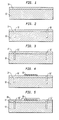
- Figure 1 shows in schematic elevation a portion of a wafer on which there is to be constructed a BAW resonator following a first step of a process to manufacture such resonator in accordance with this invention.
- Figure 2 shows in schematic elevation the same portion of the wafer shown in figure 1 following a second step of the process to manufacture such resonator in accordance with this invention.
- Figure 3 shows in schematic elevation the same portion of the wafer shown in figure 2 following a third step of the process to manufacture such resonator in accordance with this invention.
- Figure 4 shows in schematic elevation the same portion of the wafer shown in figure 3 following a fourth step of the process to manufacture such resonator in accordance with this invention.
- Figure 5 shows in schematic elevation the same portion of the wafer shown in figure 4 following a fifth step of the process to manufacture such resonator in accordance with this invention.
- Figure 6 shows in schematic elevation the same portion of the wafer shown in figure 5 following a sixth step of the process to manufacture such resonator in accordance with this invention.
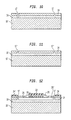
- Figure 7 shows in schematic elevation the same portion of the wafer shown in figure 6 following a seventh step of the process to manufacture such resonator in accordance with this invention.
- Figure 8 shows in schematic elevation the same portion of the wafer with the resonator structure completed.
- Figure 9 is a schematic top view of the resonator structure depicted in figure 8.
- Figure 10 shows in schematic elevation a wafer portion prepared for use in fabricating a resonator according with an alternate embodiment of this invention.
- Figure 11 shows in schematic elevation the same portion of the wafer shown in figure 10 following a second step of the process used to manufacture the alternate embodiment of the invention.
- Figure 12 shows in schematic elevation the same portion of the wafer shown in figure 11 with the alternate embodiment of the resonator completed.
- a semiconductor support 10 which is preferably a silicon wafer.
- a surface 12 of the wafer there is, preferably, deposited using conventional technology such as sputtering, an optional silicon layer to form a isolation layer 14.
- this layer is between about 2*10 -6 and 5*10 -6 meters thick.
- a trench 16 (or a series of trenches) is next etched through the isolation layer 14 and into the silicon wafer delineating a desired area 17 as better shown in figures 2 and 9. Etching of the trenches is preferably done using the well known Reactive Ion Etching technology, (RIE).
- RIE Reactive Ion Etching technology
- the trenches are next filled with low temperature oxide (LTO), to produce an etch delimiting barrier 16' which is used in later step to contain the etching of the wafer and isolation layer to within the area within the desired area 17.
- LTO low temperature oxide
- a conductive layer such as aluminum is next deposited to a typical thickness of between about 0.2*10 -6 and 0.3*10 -6 meters over the isolation layer and patterned (masked and etched according to a desired pattern using photolithography) to form a first electrode 18 on the surface of the isolation layer within the desired area 17, as shown in figure 4.
- a layer 20 of a piezoelectric material such as a layer of AIN.
- the piezoelectric AIN layer is deposited to a thickness of about 1*10 -6 and 5*10 -6 meters, preferably 2.7*10 -6 meters. However the thickness of the piezoelectric material may be different depending on the design frequency response of the resonator.
- a second conductive layer again preferably an aluminum layer is deposited over the piezoelectric layer and patterned to form a second electrode 22 substantially coextensive and over the first electrode 18, as shown in figure 7.
- connector or bond pads 24 and optionally 24' are formed also over the piezoelectric material, preferably outside the desired area 17 delimited by the trenches filled with LTO. These pads are connected to the second electrode through a conductive path 23 and 23' respectively, which is also preferably formed by photolithographic patterning simultaneously with the second electrode and bond pads.
- the bond pads serve as external connection points for accessing the resonator.
- Both the electrodes, conductive paths, bonding pads and the piezoelectric layer are preferably deposited using physical vapor deposition or sputtering.
- the size of the electrodes will vary. Typical dimensions for a square shaped electrode pair are between 100*10 -6 and 400*10 -6 meters for the sides.
- a number of vias 26 are formed, preferably by etching, through the piezoelectric material within the desired area 17.
- the vias are placed adjacent the electrodes and preferably evenly spaced all around the electrodes.
- Typical via diameters are between 5*10 -6 and 20*10 -6 meters, preferably about 10*10 -6 meters and extend through the piezoelectric layer to the surface of the isolation layer 14.
- the next step, illustrated in figure 8, is the etching of a cavity 28 under the first and second electrodes so as to isolate from the support 10 the bulk resonator formed by the three layer combination of the first electrode 18, piezoelectric layer 20 and second electrode 22.
- This is accomplished in a dry etching process by introducing through the vias 26 an etchant, which is preferably a gaseous etchant that attacks the isolation layer and may also attack the underlying support, but does not attack the piezoelectric material or the electrodes.
- a bulk acoustic resonator is formed using aluminum as the conductive material for the first and second electrodes and aluminum nitride (AlN) for the piezoelectric material.
- the support is a silicon wafer and the isolation layer is a high resistivity layer such as a silicon layer between the piezoelectric layer and the wafer surface.
- the etchant used is XeF 2 gas which attacks the silicon but does not attack the aluminum, the AIN or the LTO barriers.
- introduction of the XeF 2 etches away an area beneath the AIN layer to form a cavity 28 leaving an AIN membrane extending over the cavity to the surface of the isolation layer on the supporting wafer having an unsupported area that includes the BAW resonator over the etched cavity.
- the cavity 28 may or may not extend all the way through the isolation layer.
- the cavity depth is from about 2*10 -6 meters to about 10*10 -6 meters. Electrical connections to the bonding pads complete the resonator.
- the cavity 28' size may be designed fairly accurately by starting with a wafer 10' that already includes a bottom etch barrier 30.
- a bottom etch barrier 30 may be created by first growing or depositing a SiO 2 layer 30 over the silicon wafer surface.
- Such wafer structure has a SiO 2 layer 30 substantially parallel with its surface, as shown in the figures.
- the remainder of the manufacturing process is the same as previously described with the barrier trenches 17 extending at least to the SiO 2 layer.
- the SiO 2 layer may be thermally grown or deposited (LTO).
- LTO thermally grown or deposited
Landscapes
- Engineering & Computer Science (AREA)
- Manufacturing & Machinery (AREA)
- Microelectronics & Electronic Packaging (AREA)
- Physics & Mathematics (AREA)
- Acoustics & Sound (AREA)
- Piezo-Electric Or Mechanical Vibrators, Or Delay Or Filter Circuits (AREA)
Abstract
Description
Those having the benefit of the foregoing description of my invention may provide modifications to the embodiment herein described, such as size and shape of the resonator, cavity, vias etc. or may create filters containing more than one resonators adjacent to each other and interconnected electrically. These and other modifications are to be construed as being encompassed within the scope of the present invention as set forth in the appended claims wherein I claim:
Claims (29)
- A method for fabricating a bulk acoustic resonator on a support wherein the resonator comprises a resonator membrane and wherein the resonator is decoupled from the support by a cavity etched in the support under the resonator, the method comprising using selective etching to etch said cavity through at least one via in said resonator membrane.
- The method according to claim 1 wherein the selective etching step is selective dry etching.
- The method according to claim 2 wherein the resonator also comprises a first and a second opposing electrodes on either side of said membrane, the membrane is a piezoelectric layer extending beyond said electrodes over at least a portion of said support and the method further comprises forming a plurality of vias in said piezoelectric membrane adjacent said electrodes prior to using said selective etching to form said cavity and using said selective etching to form said cavity in said support under said first electrode.
- A method for fabricating a bulk resonator structure on a wafer comprising the steps of:(A) forming an isolation layer on an upper surface of said wafer;(B) depositing over said isolation layer a first conductive layer and patterning said first conductive layer to form a first electrode;(C) depositing over said isolation layer and first electrode a piezoelectric layer;(D) forming a second electrode over said piezoelectric layer and over said first electrode;(E) opening at least one via through said piezoelectric layer along at least one side of said first electrode and spaced therefrom; and(F) forming a cavity under said first electrode and adjacent piezoelectric layer by etching away at least a portion of said isolation layer under said first electrode and adjacent portions of piezoelectric layer, by introducing a selective etchant through said via.
- The method according to claim 4 wherein said isolation layer is a high resistivity layer.
- The method according to claim 4 wherein in step (F) the etching process is a dry etching process.
- The method according to claim 4 wherein in step (F) the cavity extends through said isolation layer into a portion of said wafer.
- The method according to claim 4 wherein step (E) comprises opening a plurality of vias and wherein said plurality of vias surrounds said first electrode.
- The method according to claim 4 wherein said wafer is a silicon wafer.
- The method according to claim 5 wherein said high resistivity layer is deposited by sputtering silicon to form a silicon layer.
- The method according to claim 10 wherein the step of forming said first electrode comprises using aluminum.
- The method according to claim 11 wherein the step of forming said piezoelectric layer comprises using AlN.
- The method according to claim 4 further comprising forming at least one etch delimiting barrier in said wafer and said isolation layer.
- The method according to claim 13 wherein said wafer is a silicon wafer, said isolation layer is silicon and said etch delimiting barrier is a low temperature oxide.
- The method according to claim 4 further comprising forming at least one conductive path connected to said second electrode.
- The method according to claim 15 wherein said conductive path is formed over said piezoelectric layer and connects said second electrode to a wire bonding pad.
- A bulk acoustic resonator comprising:(a) a support having a surface;(b) a cavity extending from the surface of said support into said support;(c) a piezoelectric membrane extending over said support and said cavity and having an area over said cavity, said membrane having an underside facing said support surface and a topside opposite said underside;(d) a first electrode adhered to said piezoelectric membrane underside over a portion of said area over said cavity;(e) a second electrode on said topside of piezoelectric membrane over said first electrode and substantially coextensive with said first electrode;(f) at least one via in said piezoelectric membrane adjacent said first and second electrodes.
- The resonator according to claim 17 wherein said support comprises a wafer and an isolation layer in contact with said underside of said piezoelectric membrane.
- The resonator according to claim 18 wherein said isolation layer is a silicon layer deposited on said wafer.
- The resonator according to claim 17 comprising a plurality of vias in said piezoelectric membrane and wherein said plurality of vias surrounds said first electrode.
- The resonator according to claim 18 wherein said wafer is a silicon wafer.
- The resonator according to claim 17 wherein said first electrode comprises aluminum.
- The resonator according to claim 17 wherein said piezoelectric layer comprises AlN.
- The resonator according to claim 17 wherein said support comprises a silicon wafer having a wafer surface, said first and said second electrodes are Al, said piezoelectric membrane is AIN and includes a plurality of vias extending therethrough located adjacent to and around said electrodes, and there is an isolation layer between said membrane undersurface and said wafer surface.
- The resonator according to claim 24 wherein said vias have a diameter between about 5*10-6 and about 20*10-6 meters
- The resonator according to claim 17 further comprising at least one etch delimiting barrier trench in said isolation layer.
- The resonator according to claim 26 wherein said support comprises a silicon wafer having a wafer surface, said isolation layer is a silicon layer over said wafer surface and said etch delimiting barrier trench comprises a low temperature oxide.
- The resonator according to claim 27 further comprising a etch barrier layer extending substantially parallel to said wafer surface in said support under said piezoelectric layer.
- The resonator according to claim 17 further comprising at least one conductive path extending from said second electrode over said piezoelectric membrane to a wire bonding path outside the membrane area over said cavity.
Applications Claiming Priority (2)
| Application Number | Priority Date | Filing Date | Title |
|---|---|---|---|
| US09/637,069 US6355498B1 (en) | 2000-08-11 | 2000-08-11 | Thin film resonators fabricated on membranes created by front side releasing |
| US637069 | 2000-08-11 |
Publications (3)
| Publication Number | Publication Date |
|---|---|
| EP1180494A2 true EP1180494A2 (en) | 2002-02-20 |
| EP1180494A3 EP1180494A3 (en) | 2003-03-26 |
| EP1180494B1 EP1180494B1 (en) | 2007-01-03 |
Family
ID=24554413
Family Applications (1)
| Application Number | Title | Priority Date | Filing Date |
|---|---|---|---|
| EP01306284A Expired - Lifetime EP1180494B1 (en) | 2000-08-11 | 2001-07-20 | Thin film resonators fabricated on membranes created by front side releasing |
Country Status (4)
| Country | Link |
|---|---|
| US (1) | US6355498B1 (en) |
| EP (1) | EP1180494B1 (en) |
| JP (1) | JP5127014B2 (en) |
| DE (1) | DE60125660T2 (en) |
Cited By (13)
| Publication number | Priority date | Publication date | Assignee | Title |
|---|---|---|---|---|
| EP1471636A1 (en) * | 2003-04-21 | 2004-10-27 | Samsung Electronics Co., Ltd. | Film bulk acoustic resonator having an air gap and a method for manufacturing the same |
| EP1469599A3 (en) * | 2003-04-18 | 2005-05-18 | Samsung Electronics Co., Ltd. | Air gap type FBAR, duplexer using the FBAR, and fabricating methods thereof |
| EP1606600A2 (en) * | 2003-03-18 | 2005-12-21 | Microgan GmbH | Sensor element with self-supporting bar structures made of group iii nitride based semiconductors |
| EP1468960A3 (en) * | 2003-04-03 | 2005-12-28 | STMicroelectronics S.A. | Tunable bimetallic microresonator formed on an isolated flexible beam |
| WO2006013119A1 (en) * | 2004-07-31 | 2006-02-09 | Robert Bosch Gmbh | Microstructured sensor and method for production thereof |
| GB2424775A (en) * | 2004-12-22 | 2006-10-04 | Agilent Technologies Inc | Thin film acoustic resonator suppresses parasitic modes to improve Q |
| US7202560B2 (en) | 2004-12-15 | 2007-04-10 | Avago Technologies Wireless Ip (Singapore) Pte. Ltd. | Wafer bonding of micro-electro mechanical systems to active circuitry |
| CN104202010A (en) * | 2014-08-28 | 2014-12-10 | 中国工程物理研究院电子工程研究所 | Hollow cavity-type film bulk acoustic resonator and production method for same |
| US9859205B2 (en) | 2011-01-31 | 2018-01-02 | Avago Technologies General Ip (Singapore) Pte. Ltd. | Semiconductor device having an airbridge and method of fabricating the same |
| EP1572577B1 (en) * | 2002-12-20 | 2018-04-18 | Soitec | Method for treating a structure to obtain an internal space |
| WO2019132931A1 (en) * | 2017-12-28 | 2019-07-04 | Intel Corporation | Group iii-nitride (iii-n) resonators and their methods of fabrication |
| CN113810012A (en) * | 2021-09-23 | 2021-12-17 | 武汉敏声新技术有限公司 | a resonator |
| WO2025242970A1 (en) * | 2024-05-23 | 2025-11-27 | Teknologian Tutkimuskeskus Vtt Oy | Pmut apparatus and its fabrication method |
Families Citing this family (100)
| Publication number | Priority date | Publication date | Assignee | Title |
|---|---|---|---|---|
| US6674291B1 (en) * | 2000-10-30 | 2004-01-06 | Agere Systems Guardian Corp. | Method and apparatus for determining and/or improving high power reliability in thin film resonator devices, and a thin film resonator device resultant therefrom |
| KR100473871B1 (en) * | 2000-11-13 | 2005-03-08 | 주식회사 엠에스솔루션 | Thin film resonator |
| US6743731B1 (en) * | 2000-11-17 | 2004-06-01 | Agere Systems Inc. | Method for making a radio frequency component and component produced thereby |
| US6714102B2 (en) * | 2001-03-01 | 2004-03-30 | Agilent Technologies, Inc. | Method of fabricating thin film bulk acoustic resonator (FBAR) and FBAR structure embodying the method |
| FR2823032B1 (en) * | 2001-04-03 | 2003-07-11 | St Microelectronics Sa | ELECTROMECHANICAL RESONATOR WITH VIBRATING BEAM |
| JP3939939B2 (en) * | 2001-07-17 | 2007-07-04 | 富士通株式会社 | Method for manufacturing piezoelectric thin film resonant element |
| US20030058107A1 (en) * | 2001-09-25 | 2003-03-27 | Ferrier Joseph A. | Personal item locator system |
| US6635519B2 (en) * | 2002-01-10 | 2003-10-21 | Agere Systems, Inc. | Structurally supported thin film resonator and method of fabrication |
| US7026235B1 (en) * | 2002-02-07 | 2006-04-11 | Cypress Semiconductor Corporation | Dual-damascene process and associated floating metal structures |
| AU2003221959A1 (en) * | 2002-04-15 | 2003-11-03 | Kevin S. Jones | Single crystal silicon membranes for microelectromechanical applications |
| KR100506729B1 (en) * | 2002-05-21 | 2005-08-08 | 삼성전기주식회사 | Film bulk acoustic resonator and method for fabrication thereof |
| US7275292B2 (en) * | 2003-03-07 | 2007-10-02 | Avago Technologies Wireless Ip (Singapore) Pte. Ltd. | Method for fabricating an acoustical resonator on a substrate |
| US7362198B2 (en) | 2003-10-30 | 2008-04-22 | Avago Technologies Wireless Ip (Singapore) Pte. Ltd | Pass bandwidth control in decoupled stacked bulk acoustic resonator devices |
| DE602004000851T2 (en) | 2003-10-30 | 2007-05-16 | Avago Technologies General Ip (Singapore) Pte. Ltd. | Acoustically coupled thin film transformer with two piezoelectric elements having opposite C-axes orientation |
| US6946928B2 (en) | 2003-10-30 | 2005-09-20 | Agilent Technologies, Inc. | Thin-film acoustically-coupled transformer |
| US7358831B2 (en) | 2003-10-30 | 2008-04-15 | Avago Technologies Wireless Ip (Singapore) Pte. Ltd. | Film bulk acoustic resonator (FBAR) devices with simplified packaging |
| US7019605B2 (en) | 2003-10-30 | 2006-03-28 | Larson Iii John D | Stacked bulk acoustic resonator band-pass filter with controllable pass bandwidth |
| US7113055B2 (en) * | 2003-11-07 | 2006-09-26 | Matsushita Electric Industrial Co., Ltd. | Piezoelectric resonator, method of manufacturing piezoelectric resonator, and filter, duplexer, and communication device using piezoelectric resonator |
| JP3944161B2 (en) * | 2003-12-25 | 2007-07-11 | 株式会社東芝 | Thin film bulk acoustic wave resonator and manufacturing method of thin film bulk acoustic wave resonator |
| US20050148065A1 (en) * | 2003-12-30 | 2005-07-07 | Intel Corporation | Biosensor utilizing a resonator having a functionalized surface |
| KR100622955B1 (en) * | 2004-04-06 | 2006-09-18 | 삼성전자주식회사 | Thin film bulk acoustic resonator and its manufacturing method |
| US7615833B2 (en) | 2004-07-13 | 2009-11-10 | Avago Technologies Wireless Ip (Singapore) Pte. Ltd. | Film bulk acoustic resonator package and method of fabricating same |
| US7388454B2 (en) | 2004-10-01 | 2008-06-17 | Avago Technologies Wireless Ip Pte Ltd | Acoustic resonator performance enhancement using alternating frame structure |
| JP4744849B2 (en) * | 2004-11-11 | 2011-08-10 | 株式会社東芝 | Semiconductor device |
| US8981876B2 (en) | 2004-11-15 | 2015-03-17 | Avago Technologies General Ip (Singapore) Pte. Ltd. | Piezoelectric resonator structures and electrical filters having frame elements |
| US20060125577A1 (en) * | 2004-12-13 | 2006-06-15 | International Semiconductor Techonology Ltd. | Acoustic resonator device and method for manufacturing the same |
| KR100692593B1 (en) * | 2005-01-24 | 2007-03-13 | 삼성전자주식회사 | MES structure, MELS structure in the form of a cantilever and a method for producing a sealed fluid channel. |
| KR100698287B1 (en) | 2005-01-31 | 2007-03-22 | 삼성전자주식회사 | Thin film bulk acoustic resonator and its manufacturing method |
| DE102005004878B4 (en) * | 2005-02-03 | 2015-01-08 | Robert Bosch Gmbh | Micromechanical capacitive pressure sensor and corresponding manufacturing method |
| US7427819B2 (en) | 2005-03-04 | 2008-09-23 | Avago Wireless Ip Pte Ltd | Film-bulk acoustic wave resonator with motion plate and method |
| US7248131B2 (en) * | 2005-03-14 | 2007-07-24 | Avago Technologies Wireless Ip (Singapore) Pte. Ltd. | Monolithic vertical integration of an acoustic resonator and electronic circuitry |
| JP2006289520A (en) * | 2005-04-06 | 2006-10-26 | Toshiba Corp | Semiconductor device using MEMS technology |
| US7369013B2 (en) * | 2005-04-06 | 2008-05-06 | Avago Technologies Wireless Ip Pte Ltd | Acoustic resonator performance enhancement using filled recessed region |
| US7436269B2 (en) * | 2005-04-18 | 2008-10-14 | Avago Technologies Wireless Ip (Singapore) Pte. Ltd. | Acoustically coupled resonators and method of making the same |
| JP4791766B2 (en) * | 2005-05-30 | 2011-10-12 | 株式会社東芝 | Semiconductor device using MEMS technology |
| US7868522B2 (en) * | 2005-09-09 | 2011-01-11 | Avago Technologies Wireless Ip (Singapore) Pte. Ltd. | Adjusted frequency temperature coefficient resonator |
| JP4713990B2 (en) * | 2005-09-13 | 2011-06-29 | 株式会社東芝 | Semiconductor device and manufacturing method thereof |
| US7391286B2 (en) | 2005-10-06 | 2008-06-24 | Avago Wireless Ip Pte Ltd | Impedance matching and parasitic capacitor resonance of FBAR resonators and coupled filters |
| US7675390B2 (en) | 2005-10-18 | 2010-03-09 | Avago Technologies Wireless Ip (Singapore) Pte. Ltd. | Acoustic galvanic isolator incorporating single decoupled stacked bulk acoustic resonator |
| US7423503B2 (en) | 2005-10-18 | 2008-09-09 | Avago Technologies Wireless Ip (Singapore) Pte. Ltd. | Acoustic galvanic isolator incorporating film acoustically-coupled transformer |
| US7737807B2 (en) * | 2005-10-18 | 2010-06-15 | Avago Technologies Wireless Ip (Singapore) Pte. Ltd. | Acoustic galvanic isolator incorporating series-connected decoupled stacked bulk acoustic resonators |
| US7425787B2 (en) | 2005-10-18 | 2008-09-16 | Avago Technologies Wireless Ip (Singapore) Pte. Ltd. | Acoustic galvanic isolator incorporating single insulated decoupled stacked bulk acoustic resonator with acoustically-resonant electrical insulator |
| US7525398B2 (en) | 2005-10-18 | 2009-04-28 | Avago Technologies General Ip (Singapore) Pte. Ltd. | Acoustically communicating data signals across an electrical isolation barrier |
| US7463499B2 (en) | 2005-10-31 | 2008-12-09 | Avago Technologies General Ip (Singapore) Pte Ltd. | AC-DC power converter |
| US7561009B2 (en) | 2005-11-30 | 2009-07-14 | Avago Technologies General Ip (Singapore) Pte. Ltd. | Film bulk acoustic resonator (FBAR) devices with temperature compensation |
| US7612636B2 (en) * | 2006-01-30 | 2009-11-03 | Avago Technologies Wireless Ip (Singapore) Pte. Ltd. | Impedance transforming bulk acoustic wave baluns |
| JP2007221588A (en) * | 2006-02-17 | 2007-08-30 | Toshiba Corp | Thin film piezoelectric resonator and manufacturing method of thin film piezoelectric resonator |
| US20070210724A1 (en) * | 2006-03-09 | 2007-09-13 | Mark Unkrich | Power adapter and DC-DC converter having acoustic transformer |
| US20070210748A1 (en) * | 2006-03-09 | 2007-09-13 | Mark Unkrich | Power supply and electronic device having integrated power supply |
| US7746677B2 (en) * | 2006-03-09 | 2010-06-29 | Avago Technologies Wireless Ip (Singapore) Pte. Ltd. | AC-DC converter circuit and power supply |
| US7479685B2 (en) * | 2006-03-10 | 2009-01-20 | Avago Technologies General Ip (Singapore) Pte. Ltd. | Electronic device on substrate with cavity and mitigated parasitic leakage path |
| US7629865B2 (en) | 2006-05-31 | 2009-12-08 | Avago Technologies Wireless Ip (Singapore) Pte. Ltd. | Piezoelectric resonator structures and electrical filters |
| FR2906238B1 (en) * | 2006-09-27 | 2008-12-19 | Commissariat Energie Atomique | METHOD FOR PRODUCING AN ELECTROMECHANICAL COMPONENT ON A PLANAR SUBSTRATE |
| US7508286B2 (en) | 2006-09-28 | 2009-03-24 | Avago Technologies Wireless Ip (Singapore) Pte. Ltd. | HBAR oscillator and method of manufacture |
| JP4047366B1 (en) * | 2007-01-30 | 2008-02-13 | 東レエンジニアリング株式会社 | Ultrasonic transducer |
| US7851333B2 (en) * | 2007-03-15 | 2010-12-14 | Infineon Technologies Ag | Apparatus comprising a device and method for producing it |
| US20090079514A1 (en) * | 2007-09-24 | 2009-03-26 | Tiberiu Jamneala | Hybrid acoustic resonator-based filters |
| US7791435B2 (en) * | 2007-09-28 | 2010-09-07 | Avago Technologies Wireless Ip (Singapore) Pte. Ltd. | Single stack coupled resonators having differential output |
| US8278802B1 (en) * | 2008-04-24 | 2012-10-02 | Rf Micro Devices, Inc. | Planarized sacrificial layer for MEMS fabrication |
| US7732977B2 (en) * | 2008-04-30 | 2010-06-08 | Avago Technologies Wireless Ip (Singapore) | Transceiver circuit for film bulk acoustic resonator (FBAR) transducers |
| US7855618B2 (en) * | 2008-04-30 | 2010-12-21 | Avago Technologies Wireless Ip (Singapore) Pte. Ltd. | Bulk acoustic resonator electrical impedance transformers |
| JP5220503B2 (en) * | 2008-07-23 | 2013-06-26 | 太陽誘電株式会社 | Elastic wave device |
| JP4636292B2 (en) * | 2008-08-27 | 2011-02-23 | 株式会社村田製作所 | Electronic component and method for manufacturing electronic component |
| US8248185B2 (en) * | 2009-06-24 | 2012-08-21 | Avago Technologies Wireless Ip (Singapore) Pte. Ltd. | Acoustic resonator structure comprising a bridge |
| US8902023B2 (en) * | 2009-06-24 | 2014-12-02 | Avago Technologies General Ip (Singapore) Pte. Ltd. | Acoustic resonator structure having an electrode with a cantilevered portion |
| US8193877B2 (en) * | 2009-11-30 | 2012-06-05 | Avago Technologies Wireless Ip (Singapore) Pte. Ltd. | Duplexer with negative phase shifting circuit |
| EP2333531A1 (en) * | 2009-12-11 | 2011-06-15 | Honeywell Romania SRL | Differential resonators for NO2 detection and methods related thereto |
| US8796904B2 (en) | 2011-10-31 | 2014-08-05 | Avago Technologies General Ip (Singapore) Pte. Ltd. | Bulk acoustic resonator comprising piezoelectric layer and inverse piezoelectric layer |
| US9243316B2 (en) | 2010-01-22 | 2016-01-26 | Avago Technologies General Ip (Singapore) Pte. Ltd. | Method of fabricating piezoelectric material with selected c-axis orientation |
| US9083302B2 (en) | 2011-02-28 | 2015-07-14 | Avago Technologies General Ip (Singapore) Pte. Ltd. | Stacked bulk acoustic resonator comprising a bridge and an acoustic reflector along a perimeter of the resonator |
| US9154112B2 (en) | 2011-02-28 | 2015-10-06 | Avago Technologies General Ip (Singapore) Pte. Ltd. | Coupled resonator filter comprising a bridge |
| US9148117B2 (en) | 2011-02-28 | 2015-09-29 | Avago Technologies General Ip (Singapore) Pte. Ltd. | Coupled resonator filter comprising a bridge and frame elements |
| US9136818B2 (en) | 2011-02-28 | 2015-09-15 | Avago Technologies General Ip (Singapore) Pte. Ltd. | Stacked acoustic resonator comprising a bridge |
| US9048812B2 (en) | 2011-02-28 | 2015-06-02 | Avago Technologies General Ip (Singapore) Pte. Ltd. | Bulk acoustic wave resonator comprising bridge formed within piezoelectric layer |
| US9425764B2 (en) | 2012-10-25 | 2016-08-23 | Avago Technologies General Ip (Singapore) Pte. Ltd. | Accoustic resonator having composite electrodes with integrated lateral features |
| US9203374B2 (en) | 2011-02-28 | 2015-12-01 | Avago Technologies General Ip (Singapore) Pte. Ltd. | Film bulk acoustic resonator comprising a bridge |
| US9444426B2 (en) | 2012-10-25 | 2016-09-13 | Avago Technologies General Ip (Singapore) Pte. Ltd. | Accoustic resonator having integrated lateral feature and temperature compensation feature |
| US8575820B2 (en) | 2011-03-29 | 2013-11-05 | Avago Technologies General Ip (Singapore) Pte. Ltd. | Stacked bulk acoustic resonator |
| US9299914B2 (en) * | 2011-04-01 | 2016-03-29 | Renesas Electronics Corporation | Semiconductor device, manufacturing method of the same, and mobile phone |
| US8350445B1 (en) | 2011-06-16 | 2013-01-08 | Avago Technologies Wireless Ip (Singapore) Pte. Ltd. | Bulk acoustic resonator comprising non-piezoelectric layer and bridge |
| US8922302B2 (en) | 2011-08-24 | 2014-12-30 | Avago Technologies General Ip (Singapore) Pte. Ltd. | Acoustic resonator formed on a pedestal |
| US9742373B2 (en) * | 2011-10-31 | 2017-08-22 | The Regents Of The University Of Michigan | Method of manufacturing a temperature-compensated micromechanical resonator |
| US9105751B2 (en) * | 2011-11-11 | 2015-08-11 | International Business Machines Corporation | Integrated semiconductor devices with single crystalline beam, methods of manufacture and design structure |
| KR101959204B1 (en) * | 2013-01-09 | 2019-07-04 | 삼성전자주식회사 | Radio frequency filter and manufacturing mathod thereof |
| JP6111966B2 (en) * | 2013-03-26 | 2017-04-12 | セイコーエプソン株式会社 | Method for manufacturing vibrator |
| CN107003302B (en) * | 2014-09-15 | 2021-11-05 | Qorvo美国公司 | Mass detection via redox coupling |
| EP3338068B1 (en) * | 2015-08-18 | 2023-03-01 | Fujifilm Sonosite, Inc. | Membrane hydrophone for high frequency ultrasound and method of manufacture |
| US11579011B2 (en) | 2016-02-19 | 2023-02-14 | Fujifilm Sonosite, Inc. | Membrane hydrophone for high frequency ultrasound and method of manufacture |
| US11070184B2 (en) * | 2016-03-11 | 2021-07-20 | Akoustis, Inc. | Piezoelectric acoustic resonator manufactured with piezoelectric thin film transfer process |
| KR20170122539A (en) | 2016-04-27 | 2017-11-06 | 삼성전기주식회사 | Bulk acoustic wave resonator and method for manufacturing the same |
| US10756703B2 (en) | 2016-08-18 | 2020-08-25 | Samsung Electro-Mechanics Co., Ltd. | Bulk acoustic wave resonator |
| US10700660B2 (en) * | 2017-10-25 | 2020-06-30 | Avago Technologies International Sales Pte. Limited | Bulk acoustic wave resonator |
| KR20200094995A (en) * | 2019-01-31 | 2020-08-10 | 삼성전기주식회사 | Bulk-acoustic wave resonator |
| WO2020191750A1 (en) * | 2019-03-28 | 2020-10-01 | 深圳市汇顶科技股份有限公司 | Crystal oscillator and manufacturing method and apparatus thereof |
| CN113086943B (en) * | 2021-03-31 | 2022-05-24 | 中国科学院半导体研究所 | Micro-nano radio frequency device and preparation method thereof |
| WO2022211104A1 (en) * | 2021-03-31 | 2022-10-06 | 株式会社村田製作所 | Elastic wave device |
| CN118575414A (en) * | 2022-07-18 | 2024-08-30 | 京东方科技集团股份有限公司 | Filter unit, preparation method thereof and electronic equipment |
| CN115178314B (en) * | 2022-08-08 | 2024-06-14 | 深圳市麦科思技术有限公司 | A micro-electromechanical system microfluidic device and a manufacturing method thereof |
| CN120021407A (en) * | 2023-11-20 | 2025-05-20 | 华为技术有限公司 | Chip and preparation method thereof, and electronic device |
| CN120017005B (en) * | 2025-04-22 | 2025-11-14 | 深圳新声半导体有限公司 | A bulk acoustic wave filter with improved membrane adhesion and its fabrication method |
Family Cites Families (62)
| Publication number | Priority date | Publication date | Assignee | Title |
|---|---|---|---|---|
| JPS58137317A (en) * | 1982-02-09 | 1983-08-15 | Nec Corp | Thin-film piezoelectric compound oscillator |
| US4556812A (en) | 1983-10-13 | 1985-12-03 | The United States Of America As Represented By The United States Department Of Energy | Acoustic resonator with Al electrodes on an AlN layer and using a GaAs substrate |
| US4502932A (en) | 1983-10-13 | 1985-03-05 | The United States Of America As Represented By The United States Department Of Energy | Acoustic resonator and method of making same |
| US4719383A (en) | 1985-05-20 | 1988-01-12 | The United States Of America As Represented By The United States Department Of Energy | Piezoelectric shear wave resonator and method of making same |
| JPS62266906A (en) * | 1986-05-15 | 1987-11-19 | Toshiba Corp | Piezoelectric thin film resonator |
| JPH0618314B2 (en) * | 1987-10-09 | 1994-03-09 | 株式会社村田製作所 | Method of manufacturing integrated resonator |
| US4988957A (en) | 1989-05-26 | 1991-01-29 | Iowa State University Research Foundation, Inc. | Electronically-tuned thin-film resonator/filter controlled oscillator |
| US5075641A (en) | 1990-12-04 | 1991-12-24 | Iowa State University Research Foundation, Inc. | High frequency oscillator comprising cointegrated thin film resonator and active device |
| US5231327A (en) | 1990-12-14 | 1993-07-27 | Tfr Technologies, Inc. | Optimized piezoelectric resonator-based networks |
| DE69206165T2 (en) | 1991-02-04 | 1996-06-05 | Motorola Inc | Hermetic packaging for frequency selective microelectronic parts. |
| US5233259A (en) | 1991-02-19 | 1993-08-03 | Westinghouse Electric Corp. | Lateral field FBAR |
| US5260596A (en) | 1991-04-08 | 1993-11-09 | Motorola, Inc. | Monolithic circuit with integrated bulk structure resonator |
| US5185589A (en) | 1991-05-17 | 1993-02-09 | Westinghouse Electric Corp. | Microwave film bulk acoustic resonator and manifolded filter bank |
| EP0546696A1 (en) | 1991-12-13 | 1993-06-16 | Hewlett-Packard Company | Process for lithography on piezoelectric films |
| US5348617A (en) | 1991-12-23 | 1994-09-20 | Iowa State University Research Foundation, Inc. | Selective etching process |
| US5232571A (en) | 1991-12-23 | 1993-08-03 | Iowa State University Research Foundation, Inc. | Aluminum nitride deposition using an AlN/Al sputter cycle technique |
| US5294898A (en) | 1992-01-29 | 1994-03-15 | Motorola, Inc. | Wide bandwidth bandpass filter comprising parallel connected piezoelectric resonators |
| US5166646A (en) | 1992-02-07 | 1992-11-24 | Motorola, Inc. | Integrated tunable resonators for use in oscillators and filters |
| US5283458A (en) | 1992-03-30 | 1994-02-01 | Trw Inc. | Temperature stable semiconductor bulk acoustic resonator |
| US5367308A (en) | 1992-05-29 | 1994-11-22 | Iowa State University Research Foundation, Inc. | Thin film resonating device |
| US5291159A (en) | 1992-07-20 | 1994-03-01 | Westinghouse Electric Corp. | Acoustic resonator filter with electrically variable center frequency and bandwidth |
| US5373268A (en) | 1993-02-01 | 1994-12-13 | Motorola, Inc. | Thin film resonator having stacked acoustic reflecting impedance matching layers and method |
| US5334960A (en) | 1993-02-16 | 1994-08-02 | Motorola, Inc. | Conjugately matched acoustic wave transducers and method |
| US5559358A (en) | 1993-05-25 | 1996-09-24 | Honeywell Inc. | Opto-electro-mechanical device or filter, process for making, and sensors made therefrom |
| US5434827A (en) | 1993-06-15 | 1995-07-18 | Hewlett-Packard Company | Matching layer for front acoustic impedance matching of clinical ultrasonic tranducers |
| US5381385A (en) | 1993-08-04 | 1995-01-10 | Hewlett-Packard Company | Electrical interconnect for multilayer transducer elements of a two-dimensional transducer array |
| US5446306A (en) | 1993-12-13 | 1995-08-29 | Trw Inc. | Thin film voltage-tuned semiconductor bulk acoustic resonator (SBAR) |
| US5587620A (en) * | 1993-12-21 | 1996-12-24 | Hewlett-Packard Company | Tunable thin film acoustic resonators and method for making the same |
| US5552655A (en) | 1994-05-04 | 1996-09-03 | Trw Inc. | Low frequency mechanical resonator |
| US5864261A (en) | 1994-05-23 | 1999-01-26 | Iowa State University Research Foundation | Multiple layer acoustical structures for thin-film resonator based circuits and systems |
| JPH08148968A (en) | 1994-11-24 | 1996-06-07 | Mitsubishi Electric Corp | Thin film piezoelectric element |
| JP3371050B2 (en) * | 1995-10-27 | 2003-01-27 | 三菱電機株式会社 | Thin film piezoelectric element |
| US5630949A (en) | 1995-06-01 | 1997-05-20 | Tfr Technologies, Inc. | Method and apparatus for fabricating a piezoelectric resonator to a resonant frequency |
| US5617065A (en) | 1995-06-29 | 1997-04-01 | Motorola, Inc. | Filter using enhanced quality factor resonator and method |
| US5596239A (en) | 1995-06-29 | 1997-01-21 | Motorola, Inc. | Enhanced quality factor resonator |
| US5692279A (en) | 1995-08-17 | 1997-12-02 | Motorola | Method of making a monolithic thin film resonator lattice filter |
| US5698928A (en) | 1995-08-17 | 1997-12-16 | Motorola, Inc. | Thin film piezoelectric arrays with enhanced coupling and fabrication methods |
| JPH0983029A (en) * | 1995-09-11 | 1997-03-28 | Mitsubishi Electric Corp | Method for manufacturing thin film piezoelectric element |
| US5702775A (en) | 1995-12-26 | 1997-12-30 | Motorola, Inc. | Microelectronic device package and method |
| US5821833A (en) | 1995-12-26 | 1998-10-13 | Tfr Technologies, Inc. | Stacked crystal filter device and method of making |
| US5646583A (en) | 1996-01-04 | 1997-07-08 | Rockwell International Corporation | Acoustic isolator having a high impedance layer of hafnium oxide |
| US5760663A (en) | 1996-08-23 | 1998-06-02 | Motorola, Inc. | Elliptic baw resonator filter and method of making the same |
| US5714917A (en) * | 1996-10-02 | 1998-02-03 | Nokia Mobile Phones Limited | Device incorporating a tunable thin film bulk acoustic resonator for performing amplitude and phase modulation |
| US6051907A (en) | 1996-10-10 | 2000-04-18 | Nokia Mobile Phones Limited | Method for performing on-wafer tuning of thin film bulk acoustic wave resonators (FBARS) |
| US5873154A (en) | 1996-10-17 | 1999-02-23 | Nokia Mobile Phones Limited | Method for fabricating a resonator having an acoustic mirror |
| US5780713A (en) | 1996-11-19 | 1998-07-14 | Hewlett-Packard Company | Post-fabrication tuning of acoustic resonators |
| US5963856A (en) | 1997-01-03 | 1999-10-05 | Lucent Technologies Inc | Wireless receiver including tunable RF bandpass filter |
| JP3301334B2 (en) * | 1997-01-31 | 2002-07-15 | 三菱電機株式会社 | Sensor element and method of manufacturing the same |
| US6087198A (en) | 1998-02-12 | 2000-07-11 | Texas Instruments Incorporated | Low cost packaging for thin-film resonators and thin-film resonator-based filters |
| US5872493A (en) | 1997-03-13 | 1999-02-16 | Nokia Mobile Phones, Ltd. | Bulk acoustic wave (BAW) filter having a top portion that includes a protective acoustic mirror |
| US5853601A (en) * | 1997-04-03 | 1998-12-29 | Northrop Grumman Corporation | Top-via etch technique for forming dielectric membranes |
| US6127768A (en) | 1997-05-09 | 2000-10-03 | Kobe Steel Usa, Inc. | Surface acoustic wave and bulk acoustic wave devices using a Zn.sub.(1-X) Yx O piezoelectric layer device |
| US5910756A (en) | 1997-05-21 | 1999-06-08 | Nokia Mobile Phones Limited | Filters and duplexers utilizing thin film stacked crystal filter structures and thin film bulk acoustic wave resonators |
| US5894647A (en) | 1997-06-30 | 1999-04-20 | Tfr Technologies, Inc. | Method for fabricating piezoelectric resonators and product |
| US5883575A (en) | 1997-08-12 | 1999-03-16 | Hewlett-Packard Company | RF-tags utilizing thin film bulk wave acoustic resonators |
| US6081171A (en) | 1998-04-08 | 2000-06-27 | Nokia Mobile Phones Limited | Monolithic filters utilizing thin film bulk acoustic wave devices and minimum passive components for controlling the shape and width of a passband response |
| US6060818A (en) | 1998-06-02 | 2000-05-09 | Hewlett-Packard Company | SBAR structures and method of fabrication of SBAR.FBAR film processing techniques for the manufacturing of SBAR/BAR filters |
| FI108583B (en) | 1998-06-02 | 2002-02-15 | Nokia Corp | resonator structures |
| US6150703A (en) * | 1998-06-29 | 2000-11-21 | Trw Inc. | Lateral mode suppression in semiconductor bulk acoustic resonator (SBAR) devices using tapered electrodes, and electrodes edge damping materials |
| US5942958A (en) | 1998-07-27 | 1999-08-24 | Tfr Technologies, Inc. | Symmetrical piezoelectric resonator filter |
| US6215375B1 (en) | 1999-03-30 | 2001-04-10 | Agilent Technologies, Inc. | Bulk acoustic wave resonator with improved lateral mode suppression |
| JP4327942B2 (en) | 1999-05-20 | 2009-09-09 | Tdk株式会社 | Thin film piezoelectric element |
-
2000
- 2000-08-11 US US09/637,069 patent/US6355498B1/en not_active Expired - Lifetime
-
2001
- 2001-07-20 EP EP01306284A patent/EP1180494B1/en not_active Expired - Lifetime
- 2001-07-20 DE DE60125660T patent/DE60125660T2/en not_active Expired - Lifetime
- 2001-08-01 JP JP2001234288A patent/JP5127014B2/en not_active Expired - Fee Related
Cited By (20)
| Publication number | Priority date | Publication date | Assignee | Title |
|---|---|---|---|---|
| EP1572577B1 (en) * | 2002-12-20 | 2018-04-18 | Soitec | Method for treating a structure to obtain an internal space |
| EP1606600A2 (en) * | 2003-03-18 | 2005-12-21 | Microgan GmbH | Sensor element with self-supporting bar structures made of group iii nitride based semiconductors |
| US7038355B2 (en) | 2003-04-03 | 2006-05-02 | Stmicroelectronics Sa | Tunable microresonator on an insulating beam deformable by the difference in thermal expansion coefficients |
| EP1468960A3 (en) * | 2003-04-03 | 2005-12-28 | STMicroelectronics S.A. | Tunable bimetallic microresonator formed on an isolated flexible beam |
| EP1469599A3 (en) * | 2003-04-18 | 2005-05-18 | Samsung Electronics Co., Ltd. | Air gap type FBAR, duplexer using the FBAR, and fabricating methods thereof |
| US7053730B2 (en) | 2003-04-18 | 2006-05-30 | Samsung Electronics Co., Ltd. | Fabricating methods for air-gap type FBARs and duplexers including securing a resonating part substrate to a cavity forming substrate |
| US7233218B2 (en) | 2003-04-18 | 2007-06-19 | Samsung Electronics Co., Ltd. | Air-gap type FBAR, and duplexer using the FBAR |
| EP1471636A1 (en) * | 2003-04-21 | 2004-10-27 | Samsung Electronics Co., Ltd. | Film bulk acoustic resonator having an air gap and a method for manufacturing the same |
| US7119638B2 (en) | 2003-04-21 | 2006-10-10 | Samsung Electronics Co., Ltd. | Film bulk acoustic resonator having an air gap and a method for manufacturing the same |
| WO2006013119A1 (en) * | 2004-07-31 | 2006-02-09 | Robert Bosch Gmbh | Microstructured sensor and method for production thereof |
| US7202560B2 (en) | 2004-12-15 | 2007-04-10 | Avago Technologies Wireless Ip (Singapore) Pte. Ltd. | Wafer bonding of micro-electro mechanical systems to active circuitry |
| GB2424775A (en) * | 2004-12-22 | 2006-10-04 | Agilent Technologies Inc | Thin film acoustic resonator suppresses parasitic modes to improve Q |
| GB2424775B (en) * | 2004-12-22 | 2009-05-13 | Agilent Technologies Inc | Acoustic resonators |
| US9859205B2 (en) | 2011-01-31 | 2018-01-02 | Avago Technologies General Ip (Singapore) Pte. Ltd. | Semiconductor device having an airbridge and method of fabricating the same |
| CN104202010A (en) * | 2014-08-28 | 2014-12-10 | 中国工程物理研究院电子工程研究所 | Hollow cavity-type film bulk acoustic resonator and production method for same |
| CN104202010B (en) * | 2014-08-28 | 2017-05-03 | 中国工程物理研究院电子工程研究所 | Hollow cavity-type film bulk acoustic resonator and production method for same |
| WO2019132931A1 (en) * | 2017-12-28 | 2019-07-04 | Intel Corporation | Group iii-nitride (iii-n) resonators and their methods of fabrication |
| CN113810012A (en) * | 2021-09-23 | 2021-12-17 | 武汉敏声新技术有限公司 | a resonator |
| CN113810012B (en) * | 2021-09-23 | 2023-11-21 | 武汉敏声新技术有限公司 | a resonator |
| WO2025242970A1 (en) * | 2024-05-23 | 2025-11-27 | Teknologian Tutkimuskeskus Vtt Oy | Pmut apparatus and its fabrication method |
Also Published As
| Publication number | Publication date |
|---|---|
| JP5127014B2 (en) | 2013-01-23 |
| DE60125660D1 (en) | 2007-02-15 |
| US6355498B1 (en) | 2002-03-12 |
| EP1180494B1 (en) | 2007-01-03 |
| EP1180494A3 (en) | 2003-03-26 |
| JP2002100953A (en) | 2002-04-05 |
| DE60125660T2 (en) | 2007-10-04 |
Similar Documents
| Publication | Publication Date | Title |
|---|---|---|
| US6355498B1 (en) | Thin film resonators fabricated on membranes created by front side releasing | |
| US6601276B2 (en) | Method for self alignment of patterned layers in thin film acoustic devices | |
| US6617751B2 (en) | Film bulk acoustic resonator and method for fabrication thereof | |
| US7622846B2 (en) | Bulk acoustic wave resonator, filter and duplexer and methods of making same | |
| US10277188B2 (en) | Switchable filters and design structures | |
| US9935600B2 (en) | Switchable filters and design structures | |
| US7939356B2 (en) | Method of manufacturing film bulk acoustic resonator using internal stress of metallic film and resonator manufactured thereby | |
| EP1299946B1 (en) | Filter and method for manufacturing the same | |
| EP1388938B1 (en) | Manufacturing film bulk acoustic resonator filters | |
| US20060290449A1 (en) | Contour-mode piezoelectric micromechanical resonators | |
| CN107026627A (en) | Orthogonal array nano-pillar FBAR and preparation method thereof and wave filter | |
| CN116846358A (en) | A filter device and its production method | |
| CN114499450B (en) | A BAW filter structure and preparation method | |
| US6846691B2 (en) | Method for making micromechanical structures having at least one lateral, small gap therebetween and micromechanical device produced thereby | |
| CN114826199A (en) | Resonator, filter and electronic device with acoustic mirror limiting structure | |
| CN116248063A (en) | A highly integrated high out-of-band rejection acoustic wave filter and its preparation method | |
| KR100480030B1 (en) | Manufacturing method of thin film bulk acoustic resonator and filter |
Legal Events
| Date | Code | Title | Description |
|---|---|---|---|
| PUAI | Public reference made under article 153(3) epc to a published international application that has entered the european phase |
Free format text: ORIGINAL CODE: 0009012 |
|
| AK | Designated contracting states |
Kind code of ref document: A2 Designated state(s): AT BE CH CY DE DK ES FI FR GB GR IE IT LI LU MC NL PT SE TR |
|
| AX | Request for extension of the european patent |
Free format text: AL;LT;LV;MK;RO;SI |
|
| PUAL | Search report despatched |
Free format text: ORIGINAL CODE: 0009013 |
|
| AK | Designated contracting states |
Kind code of ref document: A3 Designated state(s): AT BE CH CY DE DK ES FI FR GB GR IE IT LI LU MC NL PT SE TR Designated state(s): AT BE CH CY DE DK ES FI FR GB GR IE IT LI LU MC NL PT SE TR |
|
| AX | Request for extension of the european patent |
Extension state: AL LT LV MK RO SI |
|
| RIC1 | Information provided on ipc code assigned before grant |
Ipc: 7H 03H 3/02 B Ipc: 7H 03H 9/17 B Ipc: 7B 81B 3/00 A |
|
| 17P | Request for examination filed |
Effective date: 20030925 |
|
| AKX | Designation fees paid |
Designated state(s): DE FR GB |
|
| RAP1 | Party data changed (applicant data changed or rights of an application transferred) |
Owner name: AGERE SYSTEMS, INC. |
|
| 17Q | First examination report despatched |
Effective date: 20040330 |
|
| GRAP | Despatch of communication of intention to grant a patent |
Free format text: ORIGINAL CODE: EPIDOSNIGR1 |
|
| GRAS | Grant fee paid |
Free format text: ORIGINAL CODE: EPIDOSNIGR3 |
|
| GRAA | (expected) grant |
Free format text: ORIGINAL CODE: 0009210 |
|
| AK | Designated contracting states |
Kind code of ref document: B1 Designated state(s): DE FR GB |
|
| REG | Reference to a national code |
Ref country code: GB Ref legal event code: FG4D |
|
| REF | Corresponds to: |
Ref document number: 60125660 Country of ref document: DE Date of ref document: 20070215 Kind code of ref document: P |
|
| ET | Fr: translation filed | ||
| PLBE | No opposition filed within time limit |
Free format text: ORIGINAL CODE: 0009261 |
|
| STAA | Information on the status of an ep patent application or granted ep patent |
Free format text: STATUS: NO OPPOSITION FILED WITHIN TIME LIMIT |
|
| 26N | No opposition filed |
Effective date: 20071005 |
|
| PGFP | Annual fee paid to national office [announced via postgrant information from national office to epo] |
Ref country code: FR Payment date: 20140708 Year of fee payment: 14 Ref country code: GB Payment date: 20140716 Year of fee payment: 14 |
|
| REG | Reference to a national code |
Ref country code: DE Ref legal event code: R082 Ref document number: 60125660 Country of ref document: DE Representative=s name: DILG HAEUSLER SCHINDELMANN PATENTANWALTSGESELL, DE |
|
| GBPC | Gb: european patent ceased through non-payment of renewal fee |
Effective date: 20150720 |
|
| PG25 | Lapsed in a contracting state [announced via postgrant information from national office to epo] |
Ref country code: GB Free format text: LAPSE BECAUSE OF NON-PAYMENT OF DUE FEES Effective date: 20150720 |
|
| REG | Reference to a national code |
Ref country code: FR Ref legal event code: ST Effective date: 20160331 |
|
| PG25 | Lapsed in a contracting state [announced via postgrant information from national office to epo] |
Ref country code: FR Free format text: LAPSE BECAUSE OF NON-PAYMENT OF DUE FEES Effective date: 20150731 |
|
| REG | Reference to a national code |
Ref country code: DE Ref legal event code: R082 Ref document number: 60125660 Country of ref document: DE Representative=s name: DILG, HAEUSLER, SCHINDELMANN PATENTANWALTSGESE, DE Ref country code: DE Ref legal event code: R082 Ref document number: 60125660 Country of ref document: DE Representative=s name: DILG HAEUSLER SCHINDELMANN PATENTANWALTSGESELL, DE Ref country code: DE Ref legal event code: R081 Ref document number: 60125660 Country of ref document: DE Owner name: AVAGO TECHNOLOGIES GENERAL IP (SINGAPORE) PTE., SG Free format text: FORMER OWNER: AGERE SYSTEMS, INC., ALLENTOWN, PA., US Ref country code: DE Ref legal event code: R081 Ref document number: 60125660 Country of ref document: DE Owner name: AVAGO TECHNOLOGIES INTERNATIONAL SALES PTE. LI, SG Free format text: FORMER OWNER: AGERE SYSTEMS, INC., ALLENTOWN, PA., US |
|
| REG | Reference to a national code |
Ref country code: DE Ref legal event code: R081 Ref document number: 60125660 Country of ref document: DE Owner name: AVAGO TECHNOLOGIES INTERNATIONAL SALES PTE. LI, SG Free format text: FORMER OWNER: AVAGO TECHNOLOGIES GENERAL IP (SINGAPORE) PTE. LTD., SINGAPORE, SG Ref country code: DE Ref legal event code: R082 Ref document number: 60125660 Country of ref document: DE Representative=s name: DILG, HAEUSLER, SCHINDELMANN PATENTANWALTSGESE, DE Ref country code: DE Ref legal event code: R082 Ref document number: 60125660 Country of ref document: DE Representative=s name: DILG HAEUSLER SCHINDELMANN PATENTANWALTSGESELL, DE |
|
| PGFP | Annual fee paid to national office [announced via postgrant information from national office to epo] |
Ref country code: DE Payment date: 20200729 Year of fee payment: 20 |
|
| REG | Reference to a national code |
Ref country code: DE Ref legal event code: R071 Ref document number: 60125660 Country of ref document: DE |