EP1191680A2 - Circuit double de fréquence avec un dispositif de contrôle de détection pour l'amélioration des prestations du doubleur - Google Patents
Circuit double de fréquence avec un dispositif de contrôle de détection pour l'amélioration des prestations du doubleur Download PDFInfo
- Publication number
- EP1191680A2 EP1191680A2 EP01305368A EP01305368A EP1191680A2 EP 1191680 A2 EP1191680 A2 EP 1191680A2 EP 01305368 A EP01305368 A EP 01305368A EP 01305368 A EP01305368 A EP 01305368A EP 1191680 A2 EP1191680 A2 EP 1191680A2
- Authority
- EP
- European Patent Office
- Prior art keywords
- signal
- buffer
- output
- phase
- mos transistor
- Prior art date
- Legal status (The legal status is an assumption and is not a legal conclusion. Google has not performed a legal analysis and makes no representation as to the accuracy of the status listed.)
- Granted
Links
Images


Classifications
-
- H—ELECTRICITY
- H03—ELECTRONIC CIRCUITRY
- H03K—PULSE TECHNIQUE
- H03K5/00—Manipulating of pulses not covered by one of the other main groups of this subclass
- H03K5/156—Arrangements in which a continuous pulse train is transformed into a train having a desired pattern
-
- H—ELECTRICITY
- H03—ELECTRONIC CIRCUITRY
- H03B—GENERATION OF OSCILLATIONS, DIRECTLY OR BY FREQUENCY-CHANGING, BY CIRCUITS EMPLOYING ACTIVE ELEMENTS WHICH OPERATE IN A NON-SWITCHING MANNER; GENERATION OF NOISE BY SUCH CIRCUITS
- H03B19/00—Generation of oscillations by non-regenerative frequency multiplication or division of a signal from a separate source
- H03B19/06—Generation of oscillations by non-regenerative frequency multiplication or division of a signal from a separate source by means of discharge device or semiconductor device with more than two electrodes
- H03B19/14—Generation of oscillations by non-regenerative frequency multiplication or division of a signal from a separate source by means of discharge device or semiconductor device with more than two electrodes by means of a semiconductor device
Definitions
- the present invention relates to an integrated circuit, and more particularly, to a frequency doubler circuit implemented in an integrated circuit.
- Frequency doubling circuits are often used in phase locked loops for synthesizing a clock signal related in phase to an input signal.
- Frequency doubling of input signals at low frequency can be realized by use of a switching capacitor, a differential amplifier, an emitter-coupled transistor pair having different emitter area ratios (W/L), and using signal delay by logic gates and flip-flops.
- Conventional methods of doubling an input signal having a predetermined frequency in a high-frequency region include using the product of an input signal IN and a quart-shifted signal of the input signal IN, and using a micro strip line having a quarter-wave length of the input signal IN and the second harmonic frequency to the input signal IN.
- a micro strip line cannot easily be put in an IC without affecting the operations and placement of other components in the IC.
- FIG. 1 shows a conventional frequency doubler circuit, having a plurality of amplifiers 11, 13 and 19, a phase shifter 17 and a multiplier 15.
- the amplifiers 11 and 13 amplify an input signal IN, which operates at a predetermined frequency fo.
- Signal IN is output from a voltage controlled oscillator (VCO) of a phase locked loop (PLL).
- VCO voltage controlled oscillator
- PLL phase locked loop
- Multiplier 15 multiplies I with the ⁇ /2 phase-shifted signal Q.
- the output of multiplier 15 is a signal having a frequency which is double of frequency fo, i.e., 2fo. This signal is amplified by amplifier 19 and then the amplified signal is applied to a local oscillator (LO) of a mixer.
- LO local oscillator
- harmonics of the frequency fo and modulated frequency components can result due to non-linearity of active elements.
- the harmonics of the doubled frequency signal may adversely affect the sensitivity characteristic of a system.
- a frequency doubler circuit including a phase shifter, a first buffer, a second buffer, a detect-control unit, a third buffer, a fourth buffer, a multiplier and an output buffer.
- the phase shifter outputs, in response to an input signal having a predetermined frequency, a first signal which equals to the input signal in phase and a second signal which differs from the input signal in phase.
- the first buffer filters and buffers the first signal
- the second buffer filters and buffers the second signal.
- the detect-control unit detects a phase difference between the first and second signals in response to the first signal, the second signal, the output signal of the first buffer and the output signal of the second buffer, and outputs first and second control signals.
- the third buffer buffers the output signal of the first buffer in response to the first control signal
- the fourth buffer buffers the output signal of the second buffer in response to the second control signal
- the multiplier multiplies the output signals of the third and fourth buffers.
- the output buffer buffers the output signal of the multiplier.
- the second signal differs from the first signal in phase by about 90° and the output signal of the fourth buffer differs from the output signal of the third buffer in phase by about 90°.
- the filters of the first and second buffers are high pass filters, and the output filter of the output buffer is a band pass filter.
- a detection controlling apparatus for controlling, in response to an input signal having a predetermined frequency, a first signal which equals to the input signal in phase and a second signal which differs from the input signal in phase, to be multiplied
- the detection controlling apparatus including a phase detector, a converter and a driving buffer.
- the phase detector outputs a voltage which is proportional to a phase difference between the first signal and the second signal in response to the first and second signals.
- the converter generates current which is proportional to the output voltage in response to the output voltage of the phase detector network.
- the driving buffer buffers the output signal of the converter in response to the output signals of the first and second buffers, and outputs the first control signal for controlling the third buffer and the second control signal for controlling the fourth buffer.
- FIG. 2 is a schematic block diagram illustrating a frequency doubler circuit according to an embodiment of the present invention.
- the frequency doubler circuit includes a phase shifter 200, a first buffer 210, a second buffer 230, a detect-control unit 250, a third buffer 215, a fourth buffer 235, a multiplier 270 and an output buffer 290.
- the phase shifter 200 includes an amplifier 201 and a phase shift network 203.
- the amplifier 201 amplifies the signal level of an input signal IN.
- Signal IN operates at frequency fo output from a VCO (not shown).
- VCO not shown
- an input signal should be maintained at an amplitude of 500 mV or higher to obtain the minimum phase-error characteristic.
- the phase shift network 203 outputs a first signal in_I which is in phase with the input signal IN referred to herein as "in-phase signal”, and a second signal in_Q which differs in phase from the input signal IN, referred herein as "out-of-phase signal”.
- the first buffer 210 filters the first signal in_I and buffers the same.
- the first buffer 210 includes a filter 211 and an amplifier (or limiter) 213.
- the filter 211 is preferably a high pass filter (HPF) for eliminating low-frequency noise contained in the first signal in_I, and a high-pass-filtered signal is output to the amplifier 213.
- HPF high pass filter
- the second buffer 230 filters the second signal in_Q quarter-shifted from the first signal in_I and buffers the same.
- the second buffer 210 includes a filter 231 and an amplifier (or limiter) 233.
- the filter 231 is also preferably of an HPF for eliminating low-frequency noise contained in the second signal in_Q, and a high-pass-filtered signal is output to the amplifier 233.
- the detect-control unit 250 shown in FIG. 2 includes a phase detector 251, a voltage-current converter 253 and a driving buffer 255.
- the phase detector 251 detects the phase difference between the signals input in _I and in_Q and provides a voltage Vd(t), which is proportional to the phase difference between the two signals.
- the voltage Vd(t) is input to the voltage-current converter 253, which generates current proportional to Vd(t).
- the detector detects the phases and frequencies of the first signal in _I and the second signal in _Q.
- the driving buffer 255 outputs a first differential control signal I_OUT for controlling the third buffer 215 and a second differential control signal Q_OUT for controlling the fourth buffer 235, in response to a differential output signal QIIN of the first buffer 210 or a differential output signal QLIN of the second buffer 230.
- the detect-control unit 250 may include a phase-frequency detector (not shown) for detecting phase and frequency and a driving buffer 255.
- the third buffer 215 buffers the output signal QIIN of the first buffer 210 under control by the first differential control signal I_OUT of the driving buffer 255, and outputs a signal I which is in phase with the input signal IN.
- the fourth buffer 235 buffers the output signal QLIN of the second buffer 230 under control by the second differential control signal Q_OUT of the driving buffer 255, and outputs a signal Q which is out-of-phase from the input signal IN by about ⁇ /2.
- the first differential control signal I_OUT or the second differential control output signal Q_OUT controls the signal I or Q to have a phase difference of ⁇ /2.
- the third buffer 215 and the fourth buffer 235 are preferably an amplifier or a limiter.
- the amplifier 213 of the first buffer 210, the third buffer 215, the amplifier 233 of the second buffer 230 and the fourth buffer 235 convert the input signals in_I and in_Q or QIIN and QLIN into level-compensated signals I and Q.
- the amplitude matching of the input signals I and Q of the multiplier 270 minimizes the load effect in power matching with the transistor of the multiplier 270.
- the multiplier 270 multiplies the signal I of the third buffer 215, that is, cos ⁇ t, with the signal Q of the fourth buffer 235 phase-shifted from the signal I by ⁇ /2, that is, cos( ⁇ t- ⁇ /2).
- the product of cos ⁇ t ⁇ cos( ⁇ t- ⁇ /2) is cos 2 ⁇ t. That is, a signal having twice the frequency, i.e., 2fo, of the input frequency fo of the input signal IN.
- the output buffer 290 buffers the output signal cos 2 ⁇ t of the multiplier 270 and outputs the signal having a frequency of 2fo to a mixer.
- the output buffer 290 includes an output filter 291 and an amplifier 293.
- the output signal cos 2 ⁇ t contains many harmonics as well as the doubled frequency 2fo of the input signal frequency fo.
- the output filter 291 includes a band pass filter (BPF) 291 having a central frequency of 2fo for filtering the extraneous harmonics.
- the signal 2fo having passed through the BPF 291 is an LO signal of the mixer and is input to a matching amplifier 293 for pumping.
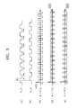
- FIG. 3 shows output waveforms of the phase detector 251 of FIG. 2.
- FIG. 3(a) shows a waveform of the first signal in_I, in which ⁇ denotes a phase difference between the first signal in_I and the second signal in_Q shown in FIG. 3(b).
- FIG. 3(c) shows the output Vd(t) of the phase detector 251 in the case where the phase difference ⁇ is ⁇ /2, and the output is indicated as a change in the DC voltage /Vd(t).
- the variation of the DC voltage /Vd(t) can be controlled by the change in the output voltage Vd(t) of the phase detector 251.
- the phase shift values are provided as the input control signal I_OUT and Q_OUT of the multiplier 270 through the driving buffer 255.
- FIG. 3(d) shows that the phase difference ⁇ is smaller than the reference phase ⁇ /2
- FIG. 3(e) shows that the phase difference ⁇ is larger than the reference phase ⁇ /2
- /Vd(t) denotes a DC level of the phase detector 251.
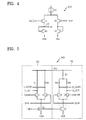
- FIG. 4 is a schematic circuit diagram of the voltage-current converter 253 of FIG. 2.
- the voltage-current converter 253 includes an nMOS transistor 43 having a drain connected to a current source 40 and a gate to which a reference voltage Vref is supplied, an nMOS transistor 47 having a drain and gate commonly connected to a source of the nMOS transistor 43 and a source connected to a ground voltage, an nMOS transistor 41 having a drain connected to the current source 40 and a gate to which the output voltage Vd(t) of the phase detector 251 is supplied, and an nMOS transistor 45 having a drain and gate commonly connected to the source of the nMOS transistor 41 and a source connected to a ground.
- An output node 49 of the voltage-current converter 253 is connected to the source of the nMOS transistor 41 and the drain of the nMOS transistor 45.
- the transistors 41 and 43 is turned on or off dependent upon Vd(t) or the reference voltage Vref.
- the transistors 41 and 43 allow constant current to flow according to the state thereof. Also, the voltage VB of the output node 49 varies according to the level of the output voltage Vd(t).
- FIG. 5 is a schematic circuit diagram of the driving buffer 255 of FIG. 2.
- the driving buffer 255 includes a first differential comparator 60 and a second differential comparator 70.
- the first differential comparator 60 outputs first differential control signals I_OUT and I_OUTB for controlling the third buffer 215 in response to the output signal VB of the voltage-current converter 253 and the differential output signals QIIN and QIINB of the amplifier 213 of the first buffer 210.
- the second differential comparator 70 outputs second differential control signals Q_OUT and Q_OUTB for controlling the fourth buffer 235 in response to the output signal VB of the voltage-current converter 253 and the differential output signals QLIN and QLINB of the amplifier 233 of the second buffer 230.
- the first differential comparator 60 includes a resistor R1 having one end connected to a power supply voltage VCC, a resistor R2 having one end connected to the power supply voltage VCC, a first transistor 51 having a collector connected to the other end of the resistor R1 and a gate to which the differential output signals QIIN and QIINB of the amplifier (or limiter) 213 of the first buffer 210 are supplied, a second transistor 53 having a collector connected to the other end of the resistor R2 and a gate to which the differential output signals QIIN and QIINB of the amplifier 213 of the first buffer 210, and an nMOS transistor 55 having a gate to which the output voltage VB of the voltage-current converter 253 is supplied and a drain commonly connected to emitters of the first and second transistors 51 and 53 and a source connected to the ground power supply VSS.
- the collector of the first transistor 51 and the collector of the second transistor 53 output the first control signals I_OUT and I_OUTB to the third buffer 215.
- the second differential comparator 70 includes a resistor R3 having one end connected to a power supply voltage VCC, a resistor R4 having one end connected to the other end of the resistor R3, a resistor R5 having one end connected to the other end of the resistor R3, a third transistor 58 having a collector connected to the other end of the resistor R4 and a gate to which the differential output signals QLIN and QLINB of the amplifier 233 of the third buffer 230 are supplied, a fourth transistor 59 having a collector connected to the other end of the resistor R5 and a gate to which the differential output signals QLIN and QLINB of the amplifier 233 of the third buffer 230, and an nMOS transistor 57 having a gate to which the output voltage VB of the voltage-current converter 253 is supplied and a drain commonly connected to emitters of the third and fourth transistors 58 and 59 and a source connected to the ground power supply VSS.
- the collector of the third transistor 58 and the collector of the fourth transistor 59 output the second control signals
- the differential output signals I_OUT and I_OUTB of the first differential comparator 60 are determined in response to the signal VB of the voltage-current converter 253, which is applied to the gate of the nMOS transistor 55, and the differential output signals QIIN and QIINB of the first buffer 210.
- the differential output signals I_OUT and I_OUTB of the first differential comparator 60 are input to the third buffer 215 to control the third buffer 215.
- the differential output signals Q_OUT and Q_OUTB of the second differential comparator 70 are determined in response to the output signal VB of the voltage-current converter 253, applied to the gate of the nMOS transistor 57, and the differential output signals QLIN and QLINB of the second buffer 230.
- the differential output signals Q_OUT and Q_OUTB of the second differential comparator 70 are input to the fourth buffer 235 to control the fourth buffer 235.
- the third buffer 215 outputs a signal I which is in phase with the input signal IN in response to the first control signals I_OUT and I_OUTB.
- the fourth buffer 235 outputs a signal Q which is out-of-phase from the input signal IN by about ⁇ /2, in response to the second control signals Q_OUT and Q_OUTB.
- the output signal I of the third buffer 215 and the output signal Q of the fourth buffer 235 are adjusted to have a phase difference of about ⁇ /2 to then be input to the multiplier 270.
- the multiplier 270 multiplies the signals I and Q and outputs a signal having a doubled frequency (2fo) of the input signal frequency (fo) to a mixer.
- the phase detector 251 outputs a voltage Vd(t), which is proportional to a phase difference between the first signal in_I and the second signal in_Q, to the voltage-current converter 253.
- the frequency doubler circuit improves the carrier to noise ratio (CNR) of harmonics relative to an LO signal of the mixer, that is, a 2fo signal.
- CNR carrier to noise ratio
- the illustrative frequency doubler circuit is implemented by an IC and improves the frequency doubling performance at a higher frequency domain by accurately adjusting a phase difference between the signals I and Q to ⁇ /2 despite changes in temperature and other parameters such as processing variations.
Landscapes
- Physics & Mathematics (AREA)
- Nonlinear Science (AREA)
- Amplifiers (AREA)
- Stabilization Of Oscillater, Synchronisation, Frequency Synthesizers (AREA)
- Manipulation Of Pulses (AREA)
- Networks Using Active Elements (AREA)
Applications Claiming Priority (2)
| Application Number | Priority Date | Filing Date | Title |
|---|---|---|---|
| KR2000056425 | 2000-09-26 | ||
| KR1020000056425A KR100351057B1 (ko) | 2000-09-26 | 2000-09-26 | 주파수의 체배성능을 향상시키기 위한 검출제어부를구비하는 주파수 체배회로 |
Publications (3)
| Publication Number | Publication Date |
|---|---|
| EP1191680A2 true EP1191680A2 (fr) | 2002-03-27 |
| EP1191680A3 EP1191680A3 (fr) | 2003-07-23 |
| EP1191680B1 EP1191680B1 (fr) | 2006-10-04 |
Family
ID=19690456
Family Applications (1)
| Application Number | Title | Priority Date | Filing Date |
|---|---|---|---|
| EP01305368A Expired - Lifetime EP1191680B1 (fr) | 2000-09-26 | 2001-06-20 | Circuit double de fréquence avec un dispositif de contrôle de détection pour l'amélioration des prestations du doubleur |
Country Status (6)
| Country | Link |
|---|---|
| US (2) | US6459311B1 (fr) |
| EP (1) | EP1191680B1 (fr) |
| JP (1) | JP2002151959A (fr) |
| KR (1) | KR100351057B1 (fr) |
| CN (2) | CN100442654C (fr) |
| DE (1) | DE60123543T2 (fr) |
Families Citing this family (17)
| Publication number | Priority date | Publication date | Assignee | Title |
|---|---|---|---|---|
| KR100663329B1 (ko) * | 2004-09-24 | 2007-01-02 | 고려대학교 산학협력단 | 주파수 체배기 |
| KR101127429B1 (ko) * | 2010-03-05 | 2012-03-26 | 한국산업기술시험원 | 주파수 디텍팅 장치 및 방법 |
| US20110229516A1 (en) * | 2010-03-18 | 2011-09-22 | The Clorox Company | Adjuvant phase inversion concentrated nanoemulsion compositions |
| US8519753B2 (en) * | 2010-12-13 | 2013-08-27 | Texas Instruments Incorporated | Frequency doubler/inverter |
| US9966937B2 (en) * | 2011-04-29 | 2018-05-08 | Marvell World Trade Ltd. | Frequency multipliers |
| CN102684604A (zh) * | 2012-05-18 | 2012-09-19 | 苏州慧飞信息科技有限公司 | 信号调制倍频器 |
| US8786330B1 (en) * | 2013-03-12 | 2014-07-22 | Infineon Technologies Ag | System and method for a frequency doubler |
| CN105048965A (zh) * | 2015-09-08 | 2015-11-11 | 电子科技大学 | 基于肖特基二极管对的毫米波双频段倍频器 |
| CN106603097B (zh) * | 2016-12-31 | 2023-08-18 | 陕西烽火电子股份有限公司 | 一种电台用展宽频响的调制线性化电路 |
| US20190004982A1 (en) * | 2017-06-29 | 2019-01-03 | SK Hynix Inc. | Buffer circuit and device including the same |
| US10749473B2 (en) * | 2017-12-20 | 2020-08-18 | Globalfoundries Inc. | Methods, apparatus, and system for a frequency doubler for a millimeter wave device |
| CN108957300A (zh) * | 2018-09-03 | 2018-12-07 | 长鑫存储技术有限公司 | 晶片测试装置及测试方法 |
| CN109787560B (zh) * | 2019-01-29 | 2023-01-10 | 石家庄市凯拓电子技术有限公司 | 一种频标倍增器 |
| RU190822U1 (ru) * | 2019-03-18 | 2019-07-15 | Евгений Борисович Колесников | Гармонический удвоитель частоты |
| KR102535454B1 (ko) * | 2020-12-29 | 2023-05-26 | 포항공과대학교 산학협력단 | 위상 천이기와 주파수 체배기를 이용한 위상 천이 방법 및 이를 수행하는 장치 |
| WO2022146037A1 (fr) | 2020-12-29 | 2022-07-07 | 포항공과대학교 산학협력단 | Procédé de déphasage à l'aide d'un déphaseur et d'un quadrupleur de fréquence et dispositif le mettant en œuvre |
| RU206321U1 (ru) * | 2021-05-24 | 2021-09-06 | Евгений Борисович Колесников | Гармонический удвоитель частоты |
Family Cites Families (18)
| Publication number | Priority date | Publication date | Assignee | Title |
|---|---|---|---|---|
| GB2196195B (en) * | 1986-09-16 | 1990-12-19 | Plessey Co Plc | Quadrature signal generator |
| FR2609851B1 (fr) * | 1987-01-20 | 1989-04-21 | Labo Electronique Physique | Dephaseur large bande |
| US5548236A (en) * | 1987-02-20 | 1996-08-20 | Pixel Instruments | Phase shifting apparatus and method with frequency multiplication |
| DE3917714A1 (de) * | 1989-05-31 | 1990-12-06 | Siemens Ag | Multiplizierschaltung |
| JPH05505297A (ja) * | 1990-12-21 | 1993-08-05 | モトローラ・インコーポレーテッド | 直角位相信号を発生するための装置および方法 |
| US5089757A (en) * | 1991-03-15 | 1992-02-18 | Maxtor Corporation | Synchronous digital detection of position error signal |
| FR2711027B1 (fr) * | 1993-10-05 | 1995-11-17 | Ebauchesfabrik Eta Ag | Circuit de correction du déphasage et des amplitudes. |
| JPH07202649A (ja) * | 1993-12-27 | 1995-08-04 | Toshiba Corp | 逓倍回路 |
| JPH07235837A (ja) * | 1994-02-24 | 1995-09-05 | Toshiba Corp | 2逓倍回路 |
| KR0145860B1 (ko) * | 1995-07-06 | 1998-12-01 | 김광호 | 디지탈/아나로그 변환기를 이용한 주파수 체배기 |
| JP2845178B2 (ja) * | 1995-08-14 | 1999-01-13 | 日本電気株式会社 | 逓倍回路 |
| CA2159762C (fr) * | 1995-10-03 | 2000-02-08 | Hugh Chow | Commande de rapport cyclique integree a un synthetiseur de frequence |
| JP2871560B2 (ja) * | 1995-11-21 | 1999-03-17 | 日本電気株式会社 | π/2移相器 |
| KR100230807B1 (ko) * | 1996-12-23 | 1999-11-15 | 김영환 | 펄스폭 제어가 가능한 주파수 체배기 |
| KR0183948B1 (ko) * | 1996-12-31 | 1999-04-15 | 삼성전자주식회사 | 주파수체배회로 |
| US6181181B1 (en) * | 1998-06-26 | 2001-01-30 | Fujitsu Limited | Phase shifter for a quadrature modulator and an image suppression mixer |
| KR100331562B1 (ko) * | 1999-11-29 | 2002-04-06 | 윤종용 | 지연 동기 루프 회로 및 내부 클럭 신호 발생 방법 |
| US6281712B1 (en) * | 2000-09-05 | 2001-08-28 | Motorola, Inc. | Phase detector with frequency steering |
-
2000
- 2000-09-26 KR KR1020000056425A patent/KR100351057B1/ko not_active Expired - Fee Related
-
2001
- 2001-05-04 US US09/849,572 patent/US6459311B1/en not_active Expired - Fee Related
- 2001-06-20 EP EP01305368A patent/EP1191680B1/fr not_active Expired - Lifetime
- 2001-06-20 DE DE60123543T patent/DE60123543T2/de not_active Expired - Fee Related
- 2001-07-10 CN CNB2004101003234A patent/CN100442654C/zh not_active Expired - Fee Related
- 2001-07-10 CN CNB011228407A patent/CN1183659C/zh not_active Expired - Fee Related
- 2001-09-11 JP JP2001275382A patent/JP2002151959A/ja active Pending
-
2002
- 2002-08-14 US US10/218,291 patent/US6535022B2/en not_active Expired - Fee Related
Also Published As
| Publication number | Publication date |
|---|---|
| CN1346175A (zh) | 2002-04-24 |
| US6535022B2 (en) | 2003-03-18 |
| US20020186062A1 (en) | 2002-12-12 |
| CN1183659C (zh) | 2005-01-05 |
| DE60123543T2 (de) | 2007-05-03 |
| CN1627629A (zh) | 2005-06-15 |
| DE60123543D1 (de) | 2006-11-16 |
| US20020036522A1 (en) | 2002-03-28 |
| EP1191680A3 (fr) | 2003-07-23 |
| CN100442654C (zh) | 2008-12-10 |
| KR20020024660A (ko) | 2002-04-01 |
| EP1191680B1 (fr) | 2006-10-04 |
| KR100351057B1 (ko) | 2002-09-05 |
| US6459311B1 (en) | 2002-10-01 |
| JP2002151959A (ja) | 2002-05-24 |
Similar Documents
| Publication | Publication Date | Title |
|---|---|---|
| US6459311B1 (en) | Frequency doubler circuit having detect-control unit for improving frequency doubling performance | |
| US5252865A (en) | Integrating phase detector | |
| US7791390B2 (en) | Phase shifter | |
| JP2847573B2 (ja) | 電圧制御発振器 | |
| US6653908B1 (en) | Oscillator circuit with automatic level control for selectively minimizing phase noise | |
| US6798678B2 (en) | Frequency voltage converter | |
| US5991612A (en) | Amplitude correction circuit | |
| EP1583220B1 (fr) | Circuit d'oscillateur avec un circuit de réduction de bruit | |
| US5515012A (en) | Very low noise, wide frequency range phase lock loop | |
| US20030197570A1 (en) | Adaptive loop gain control circuit for voltage controlled oscillator | |
| JP2008536432A (ja) | ミキサ回路 | |
| US6194973B1 (en) | Oscillator with automatic gain control | |
| US5963073A (en) | π/2 phase shifter | |
| KR100453133B1 (ko) | 구동 회로 | |
| NL1017824C2 (nl) | Lage-ruis frequentiemodulator met variabele dragerfrequentie. | |
| US7106109B2 (en) | Biasing circuit and voltage control oscillator thereof | |
| US7642867B2 (en) | Simple technique for reduction of gain in a voltage controlled oscillator | |
| US6480046B1 (en) | Transmitter apparatus and methods using frequency doubling modulation | |
| US10554199B2 (en) | Multi-stage oscillator with current voltage converters | |
| JPH09307414A (ja) | 90゜移相器 | |
| JPH0287822A (ja) | 自動位相制御回路 | |
| KR0138363B1 (ko) | 전압제어발진기 | |
| JP3490651B2 (ja) | 移相器及びそれを用いた復調器 | |
| JP2573074B2 (ja) | 電圧制御型発振器 | |
| JP2009524321A (ja) | Dcオフセットを減少させる方法 |
Legal Events
| Date | Code | Title | Description |
|---|---|---|---|
| PUAI | Public reference made under article 153(3) epc to a published international application that has entered the european phase |
Free format text: ORIGINAL CODE: 0009012 |
|
| AK | Designated contracting states |
Kind code of ref document: A2 Designated state(s): AT BE CH CY DE DK ES FI FR GB GR IE IT LI LU MC NL PT SE TR |
|
| AX | Request for extension of the european patent |
Free format text: AL;LT;LV;MK;RO;SI |
|
| RIC1 | Information provided on ipc code assigned before grant |
Ipc: 7H 03B 19/00 B Ipc: 7H 03B 19/14 A Ipc: 7H 03H 7/21 B |
|
| PUAL | Search report despatched |
Free format text: ORIGINAL CODE: 0009013 |
|
| 17P | Request for examination filed |
Effective date: 20030502 |
|
| AK | Designated contracting states |
Designated state(s): AT BE CH CY DE DK ES FI FR GB GR IE IT LI LU MC NL PT SE TR |
|
| AX | Request for extension of the european patent |
Extension state: AL LT LV MK RO SI |
|
| AKX | Designation fees paid |
Designated state(s): DE FI FR GB NL SE |
|
| 17Q | First examination report despatched |
Effective date: 20040802 |
|
| GRAP | Despatch of communication of intention to grant a patent |
Free format text: ORIGINAL CODE: EPIDOSNIGR1 |
|
| GRAS | Grant fee paid |
Free format text: ORIGINAL CODE: EPIDOSNIGR3 |
|
| GRAA | (expected) grant |
Free format text: ORIGINAL CODE: 0009210 |
|
| AK | Designated contracting states |
Kind code of ref document: B1 Designated state(s): DE FI FR GB NL SE |
|
| PG25 | Lapsed in a contracting state [announced via postgrant information from national office to epo] |
Ref country code: NL Free format text: LAPSE BECAUSE OF FAILURE TO SUBMIT A TRANSLATION OF THE DESCRIPTION OR TO PAY THE FEE WITHIN THE PRESCRIBED TIME-LIMIT Effective date: 20061004 Ref country code: FI Free format text: LAPSE BECAUSE OF FAILURE TO SUBMIT A TRANSLATION OF THE DESCRIPTION OR TO PAY THE FEE WITHIN THE PRESCRIBED TIME-LIMIT Effective date: 20061004 |
|
| REG | Reference to a national code |
Ref country code: GB Ref legal event code: FG4D |
|
| REF | Corresponds to: |
Ref document number: 60123543 Country of ref document: DE Date of ref document: 20061116 Kind code of ref document: P |
|
| PG25 | Lapsed in a contracting state [announced via postgrant information from national office to epo] |
Ref country code: SE Free format text: LAPSE BECAUSE OF FAILURE TO SUBMIT A TRANSLATION OF THE DESCRIPTION OR TO PAY THE FEE WITHIN THE PRESCRIBED TIME-LIMIT Effective date: 20070104 |
|
| NLV1 | Nl: lapsed or annulled due to failure to fulfill the requirements of art. 29p and 29m of the patents act | ||
| ET | Fr: translation filed | ||
| PLBE | No opposition filed within time limit |
Free format text: ORIGINAL CODE: 0009261 |
|
| STAA | Information on the status of an ep patent application or granted ep patent |
Free format text: STATUS: NO OPPOSITION FILED WITHIN TIME LIMIT |
|
| 26N | No opposition filed |
Effective date: 20070705 |
|
| PGFP | Annual fee paid to national office [announced via postgrant information from national office to epo] |
Ref country code: DE Payment date: 20080626 Year of fee payment: 8 |
|
| PGFP | Annual fee paid to national office [announced via postgrant information from national office to epo] |
Ref country code: FR Payment date: 20080617 Year of fee payment: 8 |
|
| PGFP | Annual fee paid to national office [announced via postgrant information from national office to epo] |
Ref country code: GB Payment date: 20080625 Year of fee payment: 8 |
|
| GBPC | Gb: european patent ceased through non-payment of renewal fee |
Effective date: 20090620 |
|
| REG | Reference to a national code |
Ref country code: FR Ref legal event code: ST Effective date: 20100226 |
|
| PG25 | Lapsed in a contracting state [announced via postgrant information from national office to epo] |
Ref country code: FR Free format text: LAPSE BECAUSE OF NON-PAYMENT OF DUE FEES Effective date: 20090630 |
|
| PG25 | Lapsed in a contracting state [announced via postgrant information from national office to epo] |
Ref country code: GB Free format text: LAPSE BECAUSE OF NON-PAYMENT OF DUE FEES Effective date: 20090620 |
|
| PG25 | Lapsed in a contracting state [announced via postgrant information from national office to epo] |
Ref country code: DE Free format text: LAPSE BECAUSE OF NON-PAYMENT OF DUE FEES Effective date: 20100101 |