EP1213729A1 - Inductor element - Google Patents
Inductor element Download PDFInfo
- Publication number
- EP1213729A1 EP1213729A1 EP00951945A EP00951945A EP1213729A1 EP 1213729 A1 EP1213729 A1 EP 1213729A1 EP 00951945 A EP00951945 A EP 00951945A EP 00951945 A EP00951945 A EP 00951945A EP 1213729 A1 EP1213729 A1 EP 1213729A1
- Authority
- EP
- European Patent Office
- Prior art keywords
- conductor
- conductors
- inductor
- inductor element
- substrate
- Prior art date
- Legal status (The legal status is an assumption and is not a legal conclusion. Google has not performed a legal analysis and makes no representation as to the accuracy of the status listed.)
- Withdrawn
Links
Images


Classifications
-
- H—ELECTRICITY
- H01—ELECTRIC ELEMENTS
- H01F—MAGNETS; INDUCTANCES; TRANSFORMERS; SELECTION OF MATERIALS FOR THEIR MAGNETIC PROPERTIES
- H01F17/00—Fixed inductances of the signal type
- H01F17/0006—Printed inductances
- H01F17/0013—Printed inductances with stacked layers
-
- H—ELECTRICITY
- H01—ELECTRIC ELEMENTS
- H01F—MAGNETS; INDUCTANCES; TRANSFORMERS; SELECTION OF MATERIALS FOR THEIR MAGNETIC PROPERTIES
- H01F17/00—Fixed inductances of the signal type
- H01F17/0006—Printed inductances
-
- H—ELECTRICITY
- H10—SEMICONDUCTOR DEVICES; ELECTRIC SOLID-STATE DEVICES NOT OTHERWISE PROVIDED FOR
- H10W—GENERIC PACKAGES, INTERCONNECTIONS, CONNECTORS OR OTHER CONSTRUCTIONAL DETAILS OF DEVICES COVERED BY CLASS H10
- H10W20/00—Interconnections in chips, wafers or substrates
- H10W20/40—Interconnections external to wafers or substrates, e.g. back-end-of-line [BEOL] metallisations or vias connecting to gate electrodes
- H10W20/497—Inductive arrangements or effects of, or between, wiring layers
-
- H—ELECTRICITY
- H01—ELECTRIC ELEMENTS
- H01F—MAGNETS; INDUCTANCES; TRANSFORMERS; SELECTION OF MATERIALS FOR THEIR MAGNETIC PROPERTIES
- H01F17/00—Fixed inductances of the signal type
- H01F17/0006—Printed inductances
- H01F2017/0073—Printed inductances with a special conductive pattern, e.g. flat spiral
Definitions
- the inductor element described above is suitable for use as a compound element that also has a capacitance component besides an inductance component. Since this inductor element has two conductors that are superimposed one on the other and its characteristics also include a capacitance component, this inductor element can be used in applications where an inductor and a capacitor are combined for making them a part of a circuit.
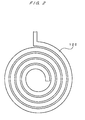
- FIG. 1 is a schematic diagram showing a planar structure of an inductor element according to the first embodiment.
- FIG. 2 is a drawing showing an upper layer of conductor included in the inductor element shown in FIG. 1.
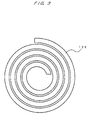
- FIG. 3 is a drawing showing a shape of a lower layer of conductor included in the inductor element shown in FIG. 1.
- a chip part of an inductor, a capacitor, or a resistor can be most easily used for the impedance element 200 described above.
- electric current flows also to another conductor by effective magnetic flux generated by the inductor conductor. Nevertheless, by terminating one end of this other conductor by an impedance element, it becomes possible to prevent unnecessary reflection in this portion, and hence, to improve characteristics.
Landscapes
- Engineering & Computer Science (AREA)
- Power Engineering (AREA)
- Microelectronics & Electronic Packaging (AREA)
- Coils Or Transformers For Communication (AREA)
- Semiconductor Integrated Circuits (AREA)
- Filters And Equalizers (AREA)
Abstract
Description
Claims (21)
- An inductor element comprising two conductors, characterized in that they are formed in piles on a substrate in the state where they are mutually insulated, wherein one conductor apart from the substrate is used as an inductor conductor, and a lead wire of this inductor conductor is led out through a gap between another conductor, being near the substrate, and the substrate.
- The inductor element according to claim 1, characterized in that three or more layers of metal layers are formed on the substrate, and the two conductors and the lead wires are formed respectively with using the metal layers which are different layers being mutually apart by one or more layers.
- The inductor element according to claim 1, characterized in that the two conductors have substantially the same shape.
- The inductor element according to claim 1, characterized in that the two conductors have long shapes.
- The inductor element according to claim 1, characterized in that the two conductors have circular shapes less than one turn.
- The inductor element according to claim 1, characterized in that the two conductors have spiral shapes each number of turns of which is one or more.
- The inductor element according to claim 1, characterized in that the two conductors each have a spiral shape having one or more turns, and the lead wire led from the inner circumferential end of the inductor conductor is made to pass between the other conductor and the substrate.
- The inductor element, characterized in that the two conductors are formed in substantially linear shapes.
- The inductor element, characterized in that the two conductors are formed in meander shapes.
- The inductor element, characterized by comprising:an inductance component of the inductor element; anda capacitance component between the two conductors.
- An inductor element comprising two conductors, characterized in that they are formed in piles on a substrate in the state where they are mutually insulated, wherein one conductor of the two conductors that is apart from the substrate is used as an inductor conductor, and further, at least an end of the other conductor of the two conductors is terminated with a predetermined impedance element.
- The inductor element according to claim 11, characterized in that it is possible to change at least one device constant of a resistor, a capacitor, and an inductor in the impedance element, and termination conditions are changed by making the device constant variable.
- The inductor element according to claim 12, characterized in that the substrate is a semiconductor substrate, and the capacitor is formed of a variable capacitance diode made of a semiconductor layer formed in the inside or outside of the semiconductor substrate.
- The inductor element according to claim 12, characterized in that the substrate is a semiconductor substrate, and the resistor is formed of a channel of an FET made of a semiconductor layer formed in the inside or outside of the semiconductor substrate.
- The inductor element according to claim 11, characterized in that the two conductors have substantially the same shape.
- The inductor element according to claim 11, characterized in that the two conductors have long shapes.
- The inductor element according to claim 11, characterized in that the two conductors have circular shapes less than one turn.
- The inductor element according to claim 11, characterized in that the two conductors have spiral shapes each number of turns of which is one or more.
- The inductor element according to claim 11, characterized in that the two conductors are formed in substantially linear shapes.
- The inductor element according to claim 11, characterized in that the two conductors are formed in meander shapes.
- The inductor element according to claim 11, characterized by comprising:an inductance component of the inductor element; anda capacitance component between the two conductors.
Applications Claiming Priority (3)
| Application Number | Priority Date | Filing Date | Title |
|---|---|---|---|
| JP11230293A JP2001052928A (en) | 1999-08-17 | 1999-08-17 | Inductor element |
| JP23029399 | 1999-08-17 | ||
| PCT/JP2000/005385 WO2001013384A1 (en) | 1999-08-17 | 2000-08-10 | Inductor element |
Publications (2)
| Publication Number | Publication Date |
|---|---|
| EP1213729A1 true EP1213729A1 (en) | 2002-06-12 |
| EP1213729A4 EP1213729A4 (en) | 2003-04-09 |
Family
ID=16905559
Family Applications (1)
| Application Number | Title | Priority Date | Filing Date |
|---|---|---|---|
| EP00951945A Withdrawn EP1213729A4 (en) | 1999-08-17 | 2000-08-10 | INDUCTOR ELEMENT |
Country Status (7)
| Country | Link |
|---|---|
| US (1) | US7046113B1 (en) |
| EP (1) | EP1213729A4 (en) |
| JP (1) | JP2001052928A (en) |
| CN (2) | CN100382208C (en) |
| HK (1) | HK1047819A1 (en) |
| TW (1) | TW457500B (en) |
| WO (1) | WO2001013384A1 (en) |
Cited By (3)
| Publication number | Priority date | Publication date | Assignee | Title |
|---|---|---|---|---|
| WO2007080531A1 (en) * | 2006-01-09 | 2007-07-19 | Nxp B.V. | Integrated circuit inductor with small floating metal structures |
| FR3082046A1 (en) * | 2018-05-30 | 2019-12-06 | Commissariat A L'energie Atomique Et Aux Energies Alternatives | INTEGRATED CIRCUIT COMPRISING AN INDUCTANCE |
| ES2736075A1 (en) * | 2018-06-21 | 2019-12-23 | Bsh Electrodomesticos Espana Sa | Induction cooking device (Machine-translation by Google Translate, not legally binding) |
Families Citing this family (44)
| Publication number | Priority date | Publication date | Assignee | Title |
|---|---|---|---|---|
| WO2005096007A1 (en) * | 2004-03-31 | 2005-10-13 | Nec Corporation | Magnetic field sensor |
| JPWO2009041304A1 (en) * | 2007-09-28 | 2011-01-27 | 日本電気株式会社 | Oscillator circuit |
| US8138876B2 (en) * | 2008-01-29 | 2012-03-20 | International Business Machines Corporation | On-chip integrated voltage-controlled variable inductor, methods of making and tuning such variable inductors, and design structures integrating such variable inductors |
| JP2010135453A (en) * | 2008-12-03 | 2010-06-17 | Renesas Electronics Corp | Semiconductor device, and method of manufacturing the same |
| KR20100078877A (en) * | 2008-12-30 | 2010-07-08 | 주식회사 동부하이텍 | Semiconductor device, and forming method thereof |
| US11476566B2 (en) * | 2009-03-09 | 2022-10-18 | Nucurrent, Inc. | Multi-layer-multi-turn structure for high efficiency wireless communication |
| US9300046B2 (en) | 2009-03-09 | 2016-03-29 | Nucurrent, Inc. | Method for manufacture of multi-layer-multi-turn high efficiency inductors |
| US9306358B2 (en) | 2009-03-09 | 2016-04-05 | Nucurrent, Inc. | Method for manufacture of multi-layer wire structure for high efficiency wireless communication |
| US9232893B2 (en) | 2009-03-09 | 2016-01-12 | Nucurrent, Inc. | Method of operation of a multi-layer-multi-turn structure for high efficiency wireless communication |
| US9444213B2 (en) | 2009-03-09 | 2016-09-13 | Nucurrent, Inc. | Method for manufacture of multi-layer wire structure for high efficiency wireless communication |
| EP4234001A3 (en) | 2009-03-09 | 2023-10-18 | NuCurrent, Inc. | System and method for wireless power transfer in implantable medical devices |
| US9439287B2 (en) | 2009-03-09 | 2016-09-06 | Nucurrent, Inc. | Multi-layer wire structure for high efficiency wireless communication |
| US9208942B2 (en) | 2009-03-09 | 2015-12-08 | Nucurrent, Inc. | Multi-layer-multi-turn structure for high efficiency wireless communication |
| US9142342B2 (en) * | 2010-05-17 | 2015-09-22 | Ronald Lambert Haner | Compact-area capacitive plates for use with spiral inductors having more than one turn |
| US20130068499A1 (en) * | 2011-09-15 | 2013-03-21 | Nucurrent Inc. | Method for Operation of Multi-Layer Wire Structure for High Efficiency Wireless Communication |
| JP6221736B2 (en) * | 2013-12-25 | 2017-11-01 | 三菱電機株式会社 | Semiconductor device |
| JP5837708B1 (en) * | 2015-02-09 | 2015-12-24 | アンリツ株式会社 | High frequency choke coil and manufacturing method thereof |
| US9941743B2 (en) | 2015-08-07 | 2018-04-10 | Nucurrent, Inc. | Single structure multi mode antenna having a unitary body construction for wireless power transmission using magnetic field coupling |
| US9941590B2 (en) | 2015-08-07 | 2018-04-10 | Nucurrent, Inc. | Single structure multi mode antenna for wireless power transmission using magnetic field coupling having magnetic shielding |
| US10636563B2 (en) | 2015-08-07 | 2020-04-28 | Nucurrent, Inc. | Method of fabricating a single structure multi mode antenna for wireless power transmission using magnetic field coupling |
| US10658847B2 (en) | 2015-08-07 | 2020-05-19 | Nucurrent, Inc. | Method of providing a single structure multi mode antenna for wireless power transmission using magnetic field coupling |
| US9960628B2 (en) | 2015-08-07 | 2018-05-01 | Nucurrent, Inc. | Single structure multi mode antenna having a single layer structure with coils on opposing sides for wireless power transmission using magnetic field coupling |
| US9941729B2 (en) | 2015-08-07 | 2018-04-10 | Nucurrent, Inc. | Single layer multi mode antenna for wireless power transmission using magnetic field coupling |
| US11205848B2 (en) | 2015-08-07 | 2021-12-21 | Nucurrent, Inc. | Method of providing a single structure multi mode antenna having a unitary body construction for wireless power transmission using magnetic field coupling |
| US10063100B2 (en) | 2015-08-07 | 2018-08-28 | Nucurrent, Inc. | Electrical system incorporating a single structure multimode antenna for wireless power transmission using magnetic field coupling |
| US9948129B2 (en) | 2015-08-07 | 2018-04-17 | Nucurrent, Inc. | Single structure multi mode antenna for wireless power transmission using magnetic field coupling having an internal switch circuit |
| US9960629B2 (en) | 2015-08-07 | 2018-05-01 | Nucurrent, Inc. | Method of operating a single structure multi mode antenna for wireless power transmission using magnetic field coupling |
| US10985465B2 (en) | 2015-08-19 | 2021-04-20 | Nucurrent, Inc. | Multi-mode wireless antenna configurations |
| US10923259B2 (en) * | 2016-07-07 | 2021-02-16 | Samsung Electro-Mechanics Co., Ltd. | Coil component |
| US10879705B2 (en) | 2016-08-26 | 2020-12-29 | Nucurrent, Inc. | Wireless connector receiver module with an electrical connector |
| US10424969B2 (en) | 2016-12-09 | 2019-09-24 | Nucurrent, Inc. | Substrate configured to facilitate through-metal energy transfer via near field magnetic coupling |
| US10958105B2 (en) | 2017-02-13 | 2021-03-23 | Nucurrent, Inc. | Transmitting base with repeater |
| US11282638B2 (en) | 2017-05-26 | 2022-03-22 | Nucurrent, Inc. | Inductor coil structures to influence wireless transmission performance |
| US11227712B2 (en) | 2019-07-19 | 2022-01-18 | Nucurrent, Inc. | Preemptive thermal mitigation for wireless power systems |
| US11271430B2 (en) | 2019-07-19 | 2022-03-08 | Nucurrent, Inc. | Wireless power transfer system with extended wireless charging range |
| US11189563B2 (en) * | 2019-08-01 | 2021-11-30 | Nanya Technology Corporation | Semiconductor structure and manufacturing method thereof |
| US11056922B1 (en) | 2020-01-03 | 2021-07-06 | Nucurrent, Inc. | Wireless power transfer system for simultaneous transfer to multiple devices |
| US11283303B2 (en) | 2020-07-24 | 2022-03-22 | Nucurrent, Inc. | Area-apportioned wireless power antenna for maximized charging volume |
| US11881716B2 (en) | 2020-12-22 | 2024-01-23 | Nucurrent, Inc. | Ruggedized communication for wireless power systems in multi-device environments |
| US11876386B2 (en) | 2020-12-22 | 2024-01-16 | Nucurrent, Inc. | Detection of foreign objects in large charging volume applications |
| US11532693B2 (en) * | 2021-01-19 | 2022-12-20 | Texas Instruments Incorporated | Passive components with improved characteristics |
| US11695302B2 (en) | 2021-02-01 | 2023-07-04 | Nucurrent, Inc. | Segmented shielding for wide area wireless power transmitter |
| US11831174B2 (en) | 2022-03-01 | 2023-11-28 | Nucurrent, Inc. | Cross talk and interference mitigation in dual wireless power transmitter |
| US12003116B2 (en) | 2022-03-01 | 2024-06-04 | Nucurrent, Inc. | Wireless power transfer system for simultaneous transfer to multiple devices with cross talk and interference mitigation |
Family Cites Families (8)
| Publication number | Priority date | Publication date | Assignee | Title |
|---|---|---|---|---|
| JPH0377360A (en) * | 1989-08-18 | 1991-04-02 | Mitsubishi Electric Corp | Semiconductor device |
| JP2946971B2 (en) * | 1992-10-28 | 1999-09-13 | 日本電気株式会社 | High frequency amplification semiconductor integrated circuit |
| JP3161147B2 (en) * | 1993-04-23 | 2001-04-25 | 松下電器産業株式会社 | Spiral inductor element |
| JP3808557B2 (en) * | 1996-08-30 | 2006-08-16 | 新潟精密株式会社 | Inductor element |
| JPH10208940A (en) * | 1997-01-26 | 1998-08-07 | T I F:Kk | Inductor element |
| JPH11273949A (en) * | 1998-03-24 | 1999-10-08 | Tif:Kk | Inductor element |
| JPH11317621A (en) * | 1998-05-07 | 1999-11-16 | Tif:Kk | LC oscillator |
| JP2001044754A (en) * | 1999-07-26 | 2001-02-16 | Niigata Seimitsu Kk | LC oscillator |
-
1999
- 1999-08-17 JP JP11230293A patent/JP2001052928A/en active Pending
-
2000
- 2000-08-10 CN CNB2005100038067A patent/CN100382208C/en not_active Expired - Fee Related
- 2000-08-10 CN CNB008117195A patent/CN1252745C/en not_active Expired - Fee Related
- 2000-08-10 TW TW089116112A patent/TW457500B/en not_active IP Right Cessation
- 2000-08-10 WO PCT/JP2000/005385 patent/WO2001013384A1/en not_active Ceased
- 2000-08-10 EP EP00951945A patent/EP1213729A4/en not_active Withdrawn
- 2000-08-10 HK HK02109256.8A patent/HK1047819A1/en unknown
- 2000-08-10 US US10/049,580 patent/US7046113B1/en not_active Expired - Fee Related
Cited By (5)
| Publication number | Priority date | Publication date | Assignee | Title |
|---|---|---|---|---|
| WO2007080531A1 (en) * | 2006-01-09 | 2007-07-19 | Nxp B.V. | Integrated circuit inductor with small floating metal structures |
| FR3082046A1 (en) * | 2018-05-30 | 2019-12-06 | Commissariat A L'energie Atomique Et Aux Energies Alternatives | INTEGRATED CIRCUIT COMPRISING AN INDUCTANCE |
| EP3579255A1 (en) | 2018-05-30 | 2019-12-11 | Commissariat à l'Énergie Atomique et aux Énergies Alternatives | Integrated circuit comprising variable inductance |
| US11017940B2 (en) | 2018-05-30 | 2021-05-25 | Commissariat A L'energie Atomique Et Aux Energies Alternatives | Integrated circuit comprising a variable inductor |
| ES2736075A1 (en) * | 2018-06-21 | 2019-12-23 | Bsh Electrodomesticos Espana Sa | Induction cooking device (Machine-translation by Google Translate, not legally binding) |
Also Published As
| Publication number | Publication date |
|---|---|
| US7046113B1 (en) | 2006-05-16 |
| CN1629988A (en) | 2005-06-22 |
| CN100382208C (en) | 2008-04-16 |
| HK1047819A1 (en) | 2003-03-07 |
| EP1213729A4 (en) | 2003-04-09 |
| WO2001013384A1 (en) | 2001-02-22 |
| TW457500B (en) | 2001-10-01 |
| JP2001052928A (en) | 2001-02-23 |
| CN1370322A (en) | 2002-09-18 |
| CN1252745C (en) | 2006-04-19 |
Similar Documents
| Publication | Publication Date | Title |
|---|---|---|
| US7046113B1 (en) | Inductor element | |
| US6664863B1 (en) | LC oscillator | |
| EP0654802B1 (en) | Variable inductance element | |
| US5760456A (en) | Integrated circuit compatible planar inductors with increased Q | |
| CA2381117C (en) | Improved multiple terminal capacitor structure | |
| US20020158306A1 (en) | Semiconductor device with a spiral inductor | |
| JP3318086B2 (en) | Variable inductance element | |
| US6922126B1 (en) | Inductor element | |
| JP3563113B2 (en) | Variable inductance element | |
| US6906610B1 (en) | Inductor element | |
| EP1211799B1 (en) | Lc oscillator | |
| US7750442B2 (en) | High-frequency switch | |
| HK1077396A1 (en) | Inductor element | |
| HK1077396B (en) | Inductor element | |
| US20250015001A1 (en) | Electronic component and circuit device | |
| EP1195780B1 (en) | Inductor element | |
| US20040089949A1 (en) | Semiconductor device with an improved transmission line | |
| JP3450408B2 (en) | LC composite element | |
| CN119560283A (en) | Inductor components and integrated circuits | |
| US20050077540A1 (en) | Integrated circuit arrangement | |
| HK1007860B (en) | Variable inductance element | |
| HK1091946A1 (en) | Integrated semiconductor inductor and method therefor | |
| HK1091946B (en) | Integrated semiconductor inductor and method therefor |
Legal Events
| Date | Code | Title | Description |
|---|---|---|---|
| PUAI | Public reference made under article 153(3) epc to a published international application that has entered the european phase |
Free format text: ORIGINAL CODE: 0009012 |
|
| 17P | Request for examination filed |
Effective date: 20020218 |
|
| AK | Designated contracting states |
Kind code of ref document: A1 Designated state(s): AT BE CH CY DE DK ES FI FR GB GR IE IT LI LU MC NL PT SE |
|
| A4 | Supplementary search report drawn up and despatched |
Effective date: 20030221 |
|
| RIC1 | Information provided on ipc code assigned before grant |
Ipc: 7H 01L 23/64 B Ipc: 7H 01F 17/00 A |
|
| RBV | Designated contracting states (corrected) |
Designated state(s): AT BE CH DE FR GB LI |
|
| RAP1 | Party data changed (applicant data changed or rights of an application transferred) |
Owner name: NIIGATA SEIMITSU CO., LTD. Owner name: RICOH COMPANY, LTD. |
|
| 17Q | First examination report despatched |
Effective date: 20071009 |
|
| STAA | Information on the status of an ep patent application or granted ep patent |
Free format text: STATUS: THE APPLICATION IS DEEMED TO BE WITHDRAWN |
|
| 18D | Application deemed to be withdrawn |
Effective date: 20100227 |