EP1214787B1 - Verfahren zur detektion und auswertung kleiner kapazitätsänderungen zur umsetzung in ein schaltsignal und kapazitiver sensor hierzu - Google Patents
Verfahren zur detektion und auswertung kleiner kapazitätsänderungen zur umsetzung in ein schaltsignal und kapazitiver sensor hierzu Download PDFInfo
- Publication number
- EP1214787B1 EP1214787B1 EP00962516A EP00962516A EP1214787B1 EP 1214787 B1 EP1214787 B1 EP 1214787B1 EP 00962516 A EP00962516 A EP 00962516A EP 00962516 A EP00962516 A EP 00962516A EP 1214787 B1 EP1214787 B1 EP 1214787B1
- Authority
- EP
- European Patent Office
- Prior art keywords
- amplifier
- signal
- positive
- voltage
- supply
- Prior art date
- Legal status (The legal status is an assumption and is not a legal conclusion. Google has not performed a legal analysis and makes no representation as to the accuracy of the status listed.)
- Expired - Lifetime
Links
- 238000000034 method Methods 0.000 title claims abstract description 17
- 238000011156 evaluation Methods 0.000 claims abstract description 17
- 238000001514 detection method Methods 0.000 claims description 5
- 230000036039 immunity Effects 0.000 claims description 5
- 230000035945 sensitivity Effects 0.000 claims description 4
- 230000003321 amplification Effects 0.000 claims description 3
- 238000006243 chemical reaction Methods 0.000 claims description 3
- 238000005516 engineering process Methods 0.000 claims description 3
- 238000003199 nucleic acid amplification method Methods 0.000 claims description 3
- 230000005540 biological transmission Effects 0.000 claims 1
- 230000007704 transition Effects 0.000 claims 1
- 230000001419 dependent effect Effects 0.000 abstract description 6
- 239000003990 capacitor Substances 0.000 description 9
- 238000010586 diagram Methods 0.000 description 8
- 230000007774 longterm Effects 0.000 description 7
- 230000005684 electric field Effects 0.000 description 3
- 239000003999 initiator Substances 0.000 description 3
- 230000010355 oscillation Effects 0.000 description 3
- 238000012935 Averaging Methods 0.000 description 2
- 238000012360 testing method Methods 0.000 description 2
- 230000015572 biosynthetic process Effects 0.000 description 1
- 238000013016 damping Methods 0.000 description 1
- 238000013461 design Methods 0.000 description 1
- 230000000694 effects Effects 0.000 description 1
- 230000001939 inductive effect Effects 0.000 description 1
- 239000000463 material Substances 0.000 description 1
- 238000000691 measurement method Methods 0.000 description 1
- 230000005855 radiation Effects 0.000 description 1
- 230000000717 retained effect Effects 0.000 description 1
- 238000010998 test method Methods 0.000 description 1
Images

Classifications
-
- H—ELECTRICITY
- H03—ELECTRONIC CIRCUITRY
- H03K—PULSE TECHNIQUE
- H03K17/00—Electronic switching or gating, i.e. not by contact-making and –breaking
- H03K17/94—Electronic switching or gating, i.e. not by contact-making and –breaking characterised by the way in which the control signals are generated
- H03K17/945—Proximity switches
- H03K17/955—Proximity switches using a capacitive detector
Definitions
- the invention relates to a method for electrical detection and evaluation small capacity changes for conversion into a switching signal, under Use of an electric amplifier, its positive or negative Supply connection to a positive or negative DC supply source and its other supply connection to a reference potential is placed, with an input to the amplifier to a detecting object relative to relatively movably arranged electrode is connected, according to the preamble of claim 1.
- the sensor electrode Part of the capacitor of the RC resonant circuit whose capacity is when approaching an object with a sufficiently large dielectric constant to change the sensor electrode is capable of, whereby the RC resonant circuit is excited to vibrate or break the vibrations and the Change in oscillation amplitude in a downstream envelope detector can be evaluated.
- Switch with such sensors have the property that the switching distance of the material properties and the nature of the body to be detected.
- the change in capacitance of an active area causes a Change in the frequency that can be evaluated.
- the proximity switch has a transmitter and a receiver for receiving from the transmitter emitted and reflected by an object radiation.
- a long-term averager forms a long-term average of the received signal, which is compared with a comparator signal.
- the comparator signal is a short-time signal which represents the instantaneous value of the received signal represents, compared with the long-term signal, in which case a comparator signal is output when the deviation of the short-term signal from Long-term signal exceeds a certain amount.
- DE 42 10 848 A1 discloses a safety device with an evaluation device Became known, a measuring point and a terminator is assigned electrically and one of the evaluation associated Display device as a function of a given by the measuring point Can operate signal. Between the measuring point and the display device is a comparator supplying a comparison means provided which the Display device controls such that at least two states of the Comparison signal to be actively signaled.
- Such sensors generally have the disadvantage that due to the Temperature dependence of the sensor no constant sensitivity is guaranteed. This can be done in a once performed adjustment of the Sensors leave the switching distance or it can be a Oscillation of the oscillator take place before an object or medium in the Response range is located; As a result, the switching distance is above the temperature range not constant. Likewise, an application-specific Adjustment of the sensor outside the specifications of the sensor required be, which can be extremely difficult to accomplish. Further show Such sensors have a large directionality, which is often disadvantageous.
- the invention is based on the object, a method and a capacitive Sensor to perform this method, which at safe evaluation of very small capacity changes a high resistance against alternating electric fields as well as a high immunity to interference and a high Temperature stability should have. Furthermore, the sensor with comparatively little effort and thus be realized inexpensively.
- the inventive method is that to the supply terminals (Plus +, minus) of the amplifier an AC signal positive and negative half-waves, such as common-mode signal or square-wave signal, is applied, so that the supply voltage of the amplifier is constant remains, however, amplifier and electrode a voltage swing in the common mode go through positive and negative half-waves of the AC signal, and upon detection of an object, a signal derived from the electrode Amplified (electrode signal) in the amplifier and this at the output of Amplifier appearing amplified AC signal then in a rectifier circuit rectified and ground potential of the AC voltage decoupled, as DC voltage or current for evaluation is used, wherein the rectified amplified AC signal to the ground potential of the size of the reactance between Electrode and object is directly dependent.
- an AC signal positive and negative half-waves such as common-mode signal or square-wave signal
- the method commutes the Amplifier between a minimum and a maximum voltage value the supply voltage UB as a function of the positive and negative Half-waves of the AC signal to ground potential back and forth ago.
- the minimum voltage value of the supply voltage UB is thereby 0 volts, based on ground potential, and the maximum voltage value 2UB.
- the AC signal of the amplifier may have a rectangular shape, whose operating frequency is approximately 20 kHz ⁇ 5 kHz.
- the amplifier has a small voltage gain factor in terms of high immunity to interference, preferably from 1: 0.5 to 1: 100, in particular 1: 1.
- a capacitive sensor In a capacitive sensor according to the preamble of claim 5 is according to the invention to the supply terminals (plus +, minus) of the amplifier an AC signal of positive and negative half waves, such as Common-mode signal or square-wave signal, applied, so that the supply voltage the amplifier remains constant, but stronger and electrode one Voltage swing in common mode of the positive and negative half waves of the Traverse AC signal, and on detection of an object amplified by the electrode signal (electrode signal) in the amplifier and this amplified AC signal appearing at the output of the amplifier then rectified in a rectifier circuit and decoupled to earth potential from the AC voltage, as DC voltage or stream is used for evaluation, the rectified, amplified AC signal to ground potential of the size of reactance between the electrode and the object is directly dependent.
- an AC signal of positive and negative half waves such as Common-mode signal or square-wave signal
- the method and the capacitive sensor have the advantage that it has a high resistance to alternating electric fields, indicating the fact because the amplifier itself is relatively insensitive because it has a having a small amplification factor.
- he can through the Applying a high control signal sufficient signal deliver. Due to a high control level and a square wave shape of the Control voltage, which gives a higher rms value, results in a good Signal-to-noise ratio between useful signal and an interference field.
- the own emission is by using a low operating frequency, for example 20 kHz, low.
- the circuit has a high noise immunity and Temperature stability and is largely over coupled interference insensitive. Likewise, the sensor with comparatively little effort realizable.
- the voltage swing depends on the Difference of the height of the DC voltage supply and the amplitude of the AC signal from.
- the amplitude of the AC signal in the positive Half wave equal to the height of the DC voltage supply UB and points in the negative half-wave ground potential or zero volts, so that the resulting Voltage lift from the voltage strokes at the supply connections (Plus +, minus) the height of the DC power supply UB has and remains constant.
- the sensor is a to the amplifier Control generator connected, which outputs the AC signal positive and negative half-waves, such as common-mode signal or square-wave signal, generated on the one hand, the control generator on the one hand directly to the negative supply connection (Negative) of the amplifier, the negative or ground input, and on the other hand via a holding capacitor Ch to the positive supply terminal Plus + of the amplifier, the plus input, is placed on the over one Diode D, the DC power supply source UB is connected.
- the negative supply connection Negative
- Ch to the positive supply terminal Plus + of the amplifier, the plus input
- Control generator is on the one hand directly to the positive supply connection + of the amplifier, plus input +, and on the other hand via a holding capacitor Ch to the negative supply connection - the amplifier, minus or Ground input -, placed, with the diode reversed poled between the Negative terminal - the amplifier and the ground is inserted so that the Amplifier at its positive or negative supply connection, plus +, Minus, from negative to positive, or vice versa, half wave one Voltage swing from single to double the level of the DC power supply UB and its negative or positive, or vice versa, Supply connection, plus +, minus-, one voltage swing from the reference potential, preferably ground potential, up to the level of the DC voltage supply UB goes through and the difference of the voltage strokes constant remains, namely in the amount of DC power supply UB.
- the output of the control generator is at an advantageous further Design simultaneously on two symmetrically constructed emitter follower in Abandoned NPN and PNP technique, the outputs of the emitter follower each to the positive and the negative supply connection, plus +, Minus, the amplifier are placed.
- control generator in an advantageous further embodiment of the sensor via an RC element to the common fork point of the emitter follower placed, wherein the resistance of the RC element, the amplitude of the Amplifier determined in relation to the total resistance.
- the amplifier of the sensor has a constant amplitude response within a given bandwidth, preferably greater than 50Hz and up to 150 kHz, so that low frequency interference fields, such as Hum fields or frequencies in the 50Hz range, or high frequencies, preferably above 150 kHz, be pruned and the Operating frequency of the control generator within this predetermined bandwidth moved without influence on the switching distance. This has the control generator frequency within limits, no influence on the switching distance.
- the amplifier has a bandpass filter on maximum gain for a given frequency, the working frequency the control generator is adjustable and changeable, so that on this way the sensitivity adjustment of the sensor is done.
- the Sensitivity adjustment namely the switching distance, done. The closer the Operating frequency of the generator at the bandpass maximum, the more sensitive becomes the sensor.
- a comparator can be connected, which is used for setting the switching distance a predetermined, constant comparator threshold having.
- the switching distance of the sensor is preferably at a constant Comparator threshold either over the predetermined height of the DC power supply UB or over the height of the output voltage of the control generator adjustable.
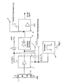
- FIGS. 1 or 2 there are basically several different ones Embodiments, wherein Figure 1 illustrates a basic constellation.
- An amplifier 1 with a relatively high-impedance input is with his Supply connections plus and minus against a given Potential, which is preferably the ground potential, in a given Common mode by a control generator 4 moves in which a voltage swing the supply connections is generated.
- a control generator 4 moves in which a voltage swing the supply connections is generated.
- an electrode 2 for example in the form of an electrode plate, connected, which is relatively movable with respect to an object 3 to be detected; the Electrode is above the input impedance of the amplifier to this tethered. In the absence or immobility of a detected Object thus runs the electrode 2 according to the common mode signal of Control generator 4 relative to the reference potential, ground potential, with.
- the current to the reference potential or ground potential is directly dependent on the size of the reactance or the capacitance between the electrode 2 and the object 3.
- the derived DC voltage is consequently a direct measure of the damping of the sensor or for the distance d of the electrode 2 to the object 3 by the relation 1 / d.
- FIG. 1 shows a schematic diagram of a capacitive electrical sensor according to the invention, as it can be used to construct a capacitive proximity switch.
- the above-described electrode 2 is connected.
- a positive DC power source with the voltage U B is connected via a diode D in the flow direction.
- a control generator 4 is connected, which generates an AC signal from positive and negative half-waves, such as common-mode signal or square wave signal.
- the AC voltage signal is applied via a holding capacitor C h to the supply voltage U B after the diode D.
- the negative supply terminal or ground terminal of the amplifier is connected directly to the output of the control generator 4, its output voltage is zero volts or ground potential in the negative half cycle, in the positive half wave, however, the potential in the amount of the supply voltage U B.
- the negative supply terminal or ground terminal of the amplifier is at zero volts or ground.
- the diode D is conductive and the amplifier 1 is supplied via the diode D with supply voltage U B , the holding capacitor C h is charged to a potential of the height of U B.
- the amplifier 1 in the negative half-wave of the AC voltage signal zero volts and in the positive half-wave to a voltage of height U B ; at the positive supply terminal plus of the amplifier 1 are in the negative half cycle of the AC signal, the voltage U B and in the positive half cycle, the voltage 2 ⁇ U B , due to the doubling of the voltage U B by the holding capacitor C h .
- the positive supply connection of the amplifier 1 thus undergoes a voltage swing from U B to 2 ⁇ U B , the negative supply connection passes through a voltage swing from zero volts to U B. This results in a voltage swing of the amplifier of constant height U B in the common mode of the positive and negative half-waves of the AC signal.
- the negative supply connection or ground connection of the amplifier is at a potential of the supply voltage U B.
- the supply voltage U B is held by the holding capacitor C h .
- the diode D is blocked, the positive supply terminal of the amplifier 1 is at a potential of 2 ⁇ U B.
- the AC signal or overlay signal at the output of the amplifier 1 at the tap 7 as the rectified, amplified AC signal to the rectifier. 5 at the tap 8 are at ground potential of the size of the reactance between electrode 2 and object 3 directly dependent and obey the Relationship 1 / d.
- the switching distance is always dependent on the comparator threshold, the amount of control voltage from the generator, the input impedance and the gain of the amplifier for each Control frequency from the generator.
- the comparator 6 can have a predefinable, have constant or changeable comparator threshold, the Example by means of an adjustable setpoint DC voltage device, for example Sollretehardts worn 11 in Figure 3, can be specified.
- the relationships between the supply terminals of the amplifier can of course be electrically reversed, so that the control generator on the one hand directly to the positive supply terminal of the amplifier, plus input, and on the other hand via a holding capacitor Ch to the negative supply terminal of the amplifier, negative or ground input, laid is, with the diode D reversed poled inserted between the negative terminal of the amplifier and the ground, so that the amplifier at its positive or negative supply terminal from the negative to the positive - or reversed - half-wave a voltage swing of one to two times the DC voltage supply U B and at its negative or positive, or vice versa, supply voltage a voltage swing from the reference potential, preferably ground potential, up to the level of the DC voltage supply U B passes and the difference of the voltage strokes remains constant, namely in Height of DC power supply U B.
- Figure 2 shows a schematic diagram of an amplifier used in a capacitive sensor with the control of the control generator 4 by two transistors NPN and PNP.
- the output signal of the control generator 4 is applied simultaneously to two symmetrically constructed emitter follower in NPN and PNP technology, wherein the outputs of the emitter follower are respectively connected to the positive and the negative supply terminal of the amplifier 1.
- the control generator 4 is connected via a series RC element R5 and C ⁇ to the common fork point 9 of the emitter follower.
- the resistance R5 of the RC element mainly determines the amplitude of the control voltage in relation to the total resistance.
- each a voltage divider R1-R3 and R4-R2 set wherein between the resistors R1 and R3 and R4 and R2 respectively Control line for the base of the transistors NPN and PNP is connected.
- the resistance R5 of the RC element mainly determines the amplitude of the amplifier 1 in relation to the total resistance.
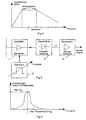
- FIG. 3 shows a block diagram of the evaluation circuit of the sensor.
- the amplifier 1 used is within a certain bandwidth, preferably greater than 50 Hz and less than 150 kHz, with a constant Amplitude response works as a broadband amplifier.
- the amplifier 1 with broadband frequency response has a constant amplitude response within a predetermined bandwidth (Figure 4), so that only very low interference fields, such as ripple fields or frequencies in the 50Hz range, or very high Frequencies are cropped, with the operating frequency of the control generator 4, which may vary slightly, within that given Bandwidth moves.
- To set the switching distance is the comparator 6 specified an adjustable comparator threshold, by means of Target DC voltage device 11 is set.
- Control frequency of the generator 4 within certain limits no effect on the Operating distance; this is only via the comparator threshold with the Setpoint DC voltage device 11 is set.
- Figure 4 shows the associated Scheme of the representation of the dependence of the gain of the Circuit in Figure 3 of the control frequency.
- FIG. 5 shows a block diagram of another used in a sensor Amplifier 1 with narrowband bandpass characteristic at variable Control generator 10.
- the amplifier 1 has a band-pass filter with maximum Gain for a given frequency, wherein the operating frequency of the Control generator 10 is adjustable and changeable.
- Narrow band means here a bandwidth of 1% to 20% of the used Center frequency; for example 10 kHz at center frequency up to 150 kHz or 1MHz at center frequency up to 10 MHz.
- the switching distance of the sensor at a constant comparator threshold can be set within certain limits either via the predeterminable level of the DC voltage supply U B or via the level of the output voltage of the control generator 4.
- the object of the invention is very much for safe evaluation in particular small capacity changes suitable.
- the usefulness of the invention lies in that it has a high resistance to alternating electric fields, which is based on the fact that the amplifier itself is relatively insensitive because he on the other hand, it has by the Applying a high control signal sufficient signal can deliver.
- the specifications of Standard EN 61000-4-3 concerning the test and measurement methods of electromagnetic Compatibility as the requirements of the Machinery Directive become.
Landscapes
- Electronic Switches (AREA)
- Transmission And Conversion Of Sensor Element Output (AREA)
- Measurement Of Resistance Or Impedance (AREA)
- Measurement Of Length, Angles, Or The Like Using Electric Or Magnetic Means (AREA)
- Burglar Alarm Systems (AREA)
Description
- Figur 1
- ein Prinzipschaltbild eines kapazitiven Sensors mit gleichtaktiger Ansteuerung eines Verstärkers unter Verwendung eines Generators, einer Diode, einem Haltekondensator sowie einer nachgeschalteten Auswertung,
- Figur 2
- ein Prinzipschaltbild eines in einem kapazitiven Sensor verwendeten weiteren Verstärkers mit der Ansteuerung durch zwei Transistoren
- Figur 3
- ein Prinzipschaltbild der Auswerteschaltung des Sensors, wobei der im Sensor verwendete Verstärker innerhalb einer gewissen Bandbreite mit konstantem Amplitudengang als Breitband-Verstärker arbeitet
- Figur 4
- die Darstellung der Abhängigkeit des Verstärkungsfaktors der Schaltung der Figur 3 von der Frequenz
- Figur 5
- ein Prinzipschaltbild eines in einem Sensor verwendeten weiteren Verstärkers mit schmalbandiger Bandpasscharakteristik bei variablem Steuergenerator und
- Figur 6
- die Darstellung der Abhängigkeit des Verstärkungsfaktors der Schaltung der Figur 5 von der Frequenz.
Claims (14)
- Verfahren zur elektrischen Detektion und Auswertung kleiner Kapazitätsänderungen zur Umsetzung in ein Schaltsignal, unter Verwendung eines elektrischen Verstärkers (1), dessen positiver oder negativer Versorgungsanschluss (Plus+, Minus-) an eine positive oder negative Gleichspannungsversorgungsquelle (UB) und dessen anderer Versorgungsanschluss (Plus+, Minus-) an ein Bezugspotential gelegt ist, wobei an den Eingang des Verstärkers eine einem zu detektierenden Objekt (3) gegenüber relativ beweglich angeordnete Elektrode (2) angeschlossen ist, dadurch gekennzeichnet, dass an die Versorgungsanschlüsse (Plus+, Minus-) des Verstärkers (1) ein Wechselspannungssignal aus positiven und negativen Halbwellen, wie Gleichtaktsignal oder Rechtecksignal, angelegt wird, so dass die Versorgungsspannung des Verstärkers konstant bleibt, jedoch Verstärker (1) und Elektrode (2) einen Spannungshub im Gleichtakt der positiven und negativen Halbwellen des Wechselspannungssignals durchlaufen, und bei Detektion eines Objektes (3) ein von der Elektrode (2) herrührendes Signal (Elektrodensignal) im Verstärker (1) verstärkt und dieses am Ausgang des Verstärkers (1) erscheinende verstärkte Wechselspannungssignal anschließend in einer Gleichrichterschaltung gleichgerichtet und gegen Erdpotential von der Wechselspannung entkoppelt, als Gleichspannung bzw. -strom zur Auswertung verwendet wird, wobei das gleichgerichtete verstärkte Wechselspannungssignal zum Erdpotential von der Größe des Blindwiderstandes zwischen Elektrode (2) und Objekt (3) direkt abhängig ist.
- Verfahren nach Anspruch 1, dadurch gekennzeichnet, dass der Verstärker zwischen einem minimalen und einem maximalen Spannungswert seiner Versorgungsspannung (UB) in Abhängigkeit von den positiven und negativen Halbwellen des Wechselspannungssignals gegenüber dem Erdpotential hin- und herpendelt.
- Verfahren nach Anspruch 1, dadurch gekennzeichnet, dass das Wechselspannungssignal des Verstärkers eine Rechteckform besitzt, deren Arbeitsfrequenz zirka 20 kHz ± 5 kHz beträgt.
- Verfahren nach Anspruch 1 oder 2, dadurch gekennzeichnet, dass der Verstärker in Bezug auf hohe Störfestigkeit einen kleinen Spannungsverstärkungsfaktor besitzt, vorzugsweise von 1:0,5 bis 1:100, insbesondere 1:1.
- Kapazitiver Sensor zur elektrischen Detektion und Auswertung kleiner Kapazitätsänderungen zur Umsetzung in ein Schaltsignal, mit einem elektrischen Verstärker (1), dessen positiver oder negativer Versorgungsanschluss (Plus+, Minus-) an eine positive oder negative Gleichspannungsversorgungsquelle (UB) und dessen anderer Versorgungsanschluss (Plus+, Minus-) an ein Bezugspotential gelegt ist, wobei an den Eingang des Verstärkers (1) eine einem zu detektierenden Objekt (3) gegenüber relativ beweglich angeordnete Elektrode (2) angeschlossen ist,
dadurch gekennzeichnet, dass an die Versorgungsanschlüsse (Plus+, Minus-) des Verstärkers (1) ein Wechselspannungssignal aus positiven und negativen Halbwellen, wie Gleichtaktsignal oder Rechtecksignal, angelegt ist, so dass die Versorgungsspannung des Verstärkers konstant bleibt, jedoch Verstärker (1) und Elektrode (2) einen Spannungshub im Gleichtakt der positiven und negativen Halbwellen des Wechselspannungssignals durchlaufen, und bei Detektion eines Objektes (3) ein von der Elektrode (2) herrührendes Signal (Elektrodensignal) im Verstärker (1) verstärkt und dieses am Ausgang des Verstärkers (1) erscheinende verstärkte Wechselspannungssignal anschließend in einer Gleichrichterschaltung gleichgerichtet und gegen Erdpotential von der Wechselspannung entkoppelt, als Gleichspannung bzw. -strom zur Auswertung verwendet wird, wobei das gleichgerichtete, verstärkte Wechselspannungssignal zum Erdpotential von der Größe des Blindwiderstandes zwischen Elektrode (2) und Objekt (3) direkt abhängig ist. - Sensor nach Anspruch 5, dadurch gekennzeichnet, dass der Spannungshub von der Differenz der Höhe der Gleichspannungsversorgung sowie der Amplitude des Wechselspannungssignals abhängt.
- Sensor nach Anspruch 5 oder 6, dadurch gekennzeichnet, dass die Amplitude des Wechselspannungssignals in der positiven Halbwelle gleich der Höhe der Gleichspannungsversorgung UB ist und in der negativen Halbwelle Massepotential bzw. Null Volt aufweist, so dass der resultierende Spannungshub aus den Spannungshüben an den Versorgungsanschlüssen (Plus+, Minus-) die Höhe der Gleichspannungsversorgung UB aufweist und konstant bleibt.
- Sensor nach Anspruch 7, dadurch gekennzeichnet, dass an den Verstärker (1) ein Steuergenerator (4) angeschlossen ist, welcher das Wechselspannungssignal aus positiven und negativen Halbwellen, wie Gleichtaktsignal oder Rechtecksignal, erzeugt, wobei der Steuergenerator (4) einerseits direkt an den negativen Versorgungsanschluss (Minus-) des Verstärkers (1), der Minus- oder Masseeingang, und andererseits über einen Haltekondensator (Ch) an den positiven Versorgungsanschluss (Plus+) des Verstärkers (1), der Pluseingang gelegt ist, an den über eine Diode (D) die Gleichspannungsversorgungsquelle UB angeschlossen ist,
oder dass der Steuergenerator (4) einerseits direkt an den positiven Versorgungsanschluss (+) des Verstärkers (1), Pluseingang (+), und andererseits über einen Haltekondensator (Ch) an den negativen Versorgungsanschluss (-) des Verstärkers (1), Minus- oder Masseeingang (-), gelegt ist,
wobei die Diode umgekehrt gepolt zwischen dem Minusanschluss (-) des Verstärkers (1) und der Masse eingefügt ist,
so dass der Verstärker (1) an seinem positiven bzw. negativen Versorgungsanschluss (Plus+, Minus-) von der negativen bis zur positiven, oder umgekehrt, Halbwelle einen Spannungshub von der einfachen bis zur doppelten Höhe der Gleichspannungsversorgung (UB) und an seinem negativen bzw. positiven, oder umgekehrt, Versorgungsanschluss (Plus+, Minus-) einen Spannungshub vom Bezugspotential, vorzugsweise Erdpotential, bis zur Höhe der Gleichspannungsversorgung (UB) durchläuft und die Differenz der Spannungshübe konstant bleibt, nämlich in Höhe der Gleichspannungsversorgung (UB). - Sensor nach Anspruch 5 oder 6 oder 7, dadurch gekennzeichnet, dass das Ausgangssignal des Steuergenerators (4) gleichzeitig auf zwei symmetrisch aufgebaute Emitterfolger in NPN- und PNP-Technik aufgegeben ist,
wobei die Ausgänge der Emitterfolger jeweils an den positiven und den negativen Versorgungsanschluss (Plus+, Minus-) des Verstärkers (1) gelegt sind. - Sensor nach Anspruch 9, dadurch gekennzeichnet, dass der Steuergenerator (4) über ein RC-Glied (R5,C∞) an den gemeinsamen Gabelpunkt der Emitterfolger gelegt ist, wobei der Widerstand (R5) des RC-Gliedes die Amplitude des Verstärkers (1) im Verhältnis zum Gesamtwiderstand bestimmt.
- Sensor nach Anspruch 5 oder 6 oder 7, dadurch gekennzeichnet, dass der Verstärker (1) einen konstanten Amplitudengang innerhalb einer vorgegebenen Bandbreite besitzt, so dass niederfrequente Störfelder, wie Brummfelder oder Frequenzen im 50Hz-Bereich, oder hohe Frequenzen, vorzugsweise oberhalb von 150 kHz, beschnitten werden und sich die Arbeitsfrequenz des Steuergenerators (4) innerhalb dieser vorgegebenen Bandbreite ohne Einfluss auf den Schaltabstand bewegt.
- Sensor nach Anspruch 5 oder 6 oder 7, dadurch gekennzeichnet, dass der Verstärker ein Bandpaßfilter aufweist mit maximaler Verstärkung für eine vorgegebene Frequenz und die Arbeitsfrequenz des Steuergenerators (4) einstellbar und veränderbar ist, so dass auf diese Weise die Empfindlichkeitseinstellung des Sensors erfolgt.
- Sensor nach einem der vorherigen Ansprüche 5 bis 12,
dadurch gekennzeichnet, dass nach dem Gleichrichter (5) eine Komparator (6) geschaltet ist, der zur Einstellung des Schaltabstandes eine vorgebbare, konstante Komparatorschwelle aufweist. - Sensor nach einem der vorherigen Ansprüche 5 bis 12,
dadurch gekennzeichnet, dass der Schaltabstand des Sensors bei konstanter Komparatorschwelle entweder über die vorgebbare Höhe der Gleichspannungsversorgung UB oder über die Höhe der Ausgangsspannung des Steuergenerators (4) einstellbar ist.
Applications Claiming Priority (3)
| Application Number | Priority Date | Filing Date | Title |
|---|---|---|---|
| DE19945330 | 1999-09-22 | ||
| DE19945330A DE19945330C2 (de) | 1999-09-22 | 1999-09-22 | Verfahren zur Detektion und Auswertung kleiner Kapazitätsänderungen zur Umsetzung in ein Schaltsignal und kapazitiver Sensor hierzu |
| PCT/EP2000/009258 WO2001022586A1 (de) | 1999-09-22 | 2000-09-21 | Verfahren zur detektion und auswertung kleiner kapazitätsänderungen zur umsetzung in ein schaltsignal und kapazitiver sensor hierzu |
Publications (2)
| Publication Number | Publication Date |
|---|---|
| EP1214787A1 EP1214787A1 (de) | 2002-06-19 |
| EP1214787B1 true EP1214787B1 (de) | 2003-06-18 |
Family
ID=7922848
Family Applications (1)
| Application Number | Title | Priority Date | Filing Date |
|---|---|---|---|
| EP00962516A Expired - Lifetime EP1214787B1 (de) | 1999-09-22 | 2000-09-21 | Verfahren zur detektion und auswertung kleiner kapazitätsänderungen zur umsetzung in ein schaltsignal und kapazitiver sensor hierzu |
Country Status (5)
| Country | Link |
|---|---|
| EP (1) | EP1214787B1 (de) |
| AT (1) | ATE243389T1 (de) |
| AU (1) | AU7421000A (de) |
| DE (2) | DE19945330C2 (de) |
| WO (1) | WO2001022586A1 (de) |
Cited By (2)
| Publication number | Priority date | Publication date | Assignee | Title |
|---|---|---|---|---|
| EP2642663A1 (de) | 2012-03-20 | 2013-09-25 | Pepperl + Fuchs GmbH | Sensor und Verfahren zum Nachweisen eines Objekts |
| DE102014224222A1 (de) * | 2014-11-27 | 2016-01-07 | Carl Zeiss Smt Gmbh | Kapazitiver Messsensor und Positions-Messeinrichtung zur Ermittlung einer Position eines Messobjekts sowie Positioniervorrichtung mit einem derartigen Messsensor |
Families Citing this family (5)
| Publication number | Priority date | Publication date | Assignee | Title |
|---|---|---|---|---|
| DE102005057558B4 (de) | 2005-11-30 | 2012-02-02 | Sie Sensorik Industrie-Elektronik Gmbh | Sensor zur berührungslosen Detektion des Füllstandes eines flüssigen und anhaftenden Mediums hoher Leitfähigkeit, insbesonere Blut, durch eine nichtmetallische Behälterwand eines Behälters und Verfahren hierzu |
| DE102009017011A1 (de) | 2009-04-14 | 2010-10-28 | Balluff Gmbh | Schaltungsanordnung zur Bestimmung einer Messkapazität |
| DE102015223636B4 (de) * | 2014-12-12 | 2016-11-17 | Ifm Electronic Gmbh | Schaltung für einen Analogsensor |
| DE102014225769B4 (de) * | 2014-12-12 | 2016-11-10 | Ifm Electronic Gmbh | Schaltung für einen Analogsensor |
| DE102022131053B3 (de) | 2022-11-23 | 2024-04-04 | Balluff Gmbh | Schaltungsanordnungen zur Messung wenigstens einer Kapazität |
Family Cites Families (10)
| Publication number | Priority date | Publication date | Assignee | Title |
|---|---|---|---|---|
| US3694741A (en) * | 1970-10-28 | 1972-09-26 | Ade Corp | Coupled inductance impedance measuring circuit with increased sensitivity and frequency independence |
| DE3143114A1 (de) * | 1980-11-07 | 1982-07-15 | Mestra AG, 4153 Reinach | Verfahren und schaltung zur messung von kapazitaeten |
| DE3408261A1 (de) * | 1984-03-07 | 1985-09-19 | Hansa Metallwerke Ag, 7000 Stuttgart | Annaeherungsschalter sowie steuerschaltungsanordnung hierfuer |
| DD267239A1 (de) * | 1987-12-24 | 1989-04-26 | Polygraph Leipzig | Kapazitive sensoreinrichtung |
| DE3911009A1 (de) * | 1989-04-05 | 1990-10-11 | Ifm Electronic Gmbh | Elektronischer annaeherungsschalter |
| DE4210848A1 (de) * | 1992-02-19 | 1993-08-26 | Beckhausen Karlheinz | Sicherheitseinrichtung |
| EP0723166B1 (de) * | 1995-01-18 | 2000-03-08 | Carlo Gavazzi Services AG | Kapazitiver Sensor |
| DE19536198B4 (de) * | 1995-09-28 | 2006-03-30 | Endress + Hauser Gmbh + Co. Kg | Kapazitiver Schalter |
| DE19701899C2 (de) * | 1996-01-21 | 2001-01-25 | Ifm Electronic Gmbh | Schaltungsanordnung und Verfahren zur Erfassung der Kapazität bzw. einer Kapazitätsänderung eines kapazitiven Schaltungs- oder Bauelementes |
| DE19836054A1 (de) * | 1998-08-10 | 2000-02-17 | Bosch Gmbh Robert | Meßschaltung |
-
1999
- 1999-09-22 DE DE19945330A patent/DE19945330C2/de not_active Expired - Fee Related
-
2000
- 2000-09-21 DE DE50002606T patent/DE50002606D1/de not_active Expired - Lifetime
- 2000-09-21 AU AU74210/00A patent/AU7421000A/en not_active Abandoned
- 2000-09-21 AT AT00962516T patent/ATE243389T1/de not_active IP Right Cessation
- 2000-09-21 EP EP00962516A patent/EP1214787B1/de not_active Expired - Lifetime
- 2000-09-21 WO PCT/EP2000/009258 patent/WO2001022586A1/de not_active Ceased
Cited By (2)
| Publication number | Priority date | Publication date | Assignee | Title |
|---|---|---|---|---|
| EP2642663A1 (de) | 2012-03-20 | 2013-09-25 | Pepperl + Fuchs GmbH | Sensor und Verfahren zum Nachweisen eines Objekts |
| DE102014224222A1 (de) * | 2014-11-27 | 2016-01-07 | Carl Zeiss Smt Gmbh | Kapazitiver Messsensor und Positions-Messeinrichtung zur Ermittlung einer Position eines Messobjekts sowie Positioniervorrichtung mit einem derartigen Messsensor |
Also Published As
| Publication number | Publication date |
|---|---|
| DE19945330C2 (de) | 2002-10-31 |
| ATE243389T1 (de) | 2003-07-15 |
| AU7421000A (en) | 2001-04-24 |
| DE50002606D1 (de) | 2003-07-24 |
| EP1214787A1 (de) | 2002-06-19 |
| WO2001022586A1 (de) | 2001-03-29 |
| DE19945330A1 (de) | 2001-04-26 |
Similar Documents
| Publication | Publication Date | Title |
|---|---|---|
| DE10131243C1 (de) | Kapazitiver Näherungsschalter | |
| DE69405168T2 (de) | Kapazitive Sensorschaltung | |
| DE112011101945T5 (de) | Robustes kapazitives Messsystern | |
| DE19851506C1 (de) | Auswerteverfahren für kapazitive Sensoren | |
| EP0551606B1 (de) | Metallsuchdetektor | |
| DE2946062A1 (de) | Messeinrichtung zur kontaktfreien erfassung des abstandes einer metallischen flaeche von einer gegenflaeche und auswerteverfahren fuer eine solche messeinrichtu ng | |
| EP1194740B1 (de) | Elektrischer sensor zur messung einer kapazitätsänderung und umsetzung in ein spannungssignal | |
| WO2019121974A1 (de) | Elektronisches gerät mit induktivem sensor | |
| DE19945330C2 (de) | Verfahren zur Detektion und Auswertung kleiner Kapazitätsänderungen zur Umsetzung in ein Schaltsignal und kapazitiver Sensor hierzu | |
| EP2642663B1 (de) | Sensor und Verfahren zum Nachweisen eines Objekts | |
| EP0249681A1 (de) | Messvorrichtung zur intrakardialen Erfassung der Blutsauerstoffsättigung | |
| EP0668987B1 (de) | Koordinatenmessgerät mit einem taster in form eines festkörperschwingers | |
| DE602005003117T2 (de) | System und verfahren zum prüfen mechanischer stücke mit drahtloser signalübertragung | |
| DE2106719B2 (de) | Positionsmelder | |
| DE4433677B4 (de) | Verfahren zur Überwachung eines sich bewegenden Mediums unter Verwendung eines elektrischen Sensors und Vorrichtung hierzu | |
| EP0165258B2 (de) | Magnetometer mit zeitverschlüsselung | |
| EP1007909A1 (de) | Magnetischer resonanzsensor | |
| DE1954136C3 (de) | Schaltungsanordnung zur Überwachung einer periodischen elektrischen Meßspannung vorgegebener Frequenz | |
| DE3429326C2 (de) | ||
| DE19523373C2 (de) | Magnetischer Resonanzsensor | |
| EP4513199B1 (de) | Näherungsschalter zur geschwindigkeitsmessung eines messobjekts | |
| DE2157824A1 (de) | Vorrichtung zur feststellung von bewegten metallteilen | |
| EP1626609B1 (de) | Verfahren und Vorrichtung zum Ermitteln eines Zustands einer Gebereinrichtung | |
| DE19753186C2 (de) | Verfahren und Anordnung zur Feststellung der elektrischen Feldstärke in TEM-Zellen | |
| EP0267302B1 (de) | Schaltungseinrichtung für eine Meldeeinrichtung zur Raumüberwachung |
Legal Events
| Date | Code | Title | Description |
|---|---|---|---|
| PUAI | Public reference made under article 153(3) epc to a published international application that has entered the european phase |
Free format text: ORIGINAL CODE: 0009012 |
|
| 17P | Request for examination filed |
Effective date: 20010813 |
|
| AK | Designated contracting states |
Kind code of ref document: A1 Designated state(s): AT BE CH CY DE DK ES FI FR GB GR IE IT LI LU MC NL PT SE |
|
| AX | Request for extension of the european patent |
Free format text: LT;LV;RO |
|
| GRAH | Despatch of communication of intention to grant a patent |
Free format text: ORIGINAL CODE: EPIDOS IGRA |
|
| GRAH | Despatch of communication of intention to grant a patent |
Free format text: ORIGINAL CODE: EPIDOS IGRA |
|
| GRAA | (expected) grant |
Free format text: ORIGINAL CODE: 0009210 |
|
| AK | Designated contracting states |
Designated state(s): AT BE CH CY DE DK ES FI FR GB GR IE IT LI LU MC NL PT SE |
|
| PG25 | Lapsed in a contracting state [announced via postgrant information from national office to epo] |
Ref country code: IT Free format text: LAPSE BECAUSE OF FAILURE TO SUBMIT A TRANSLATION OF THE DESCRIPTION OR TO PAY THE FEE WITHIN THE PRESCRIBED TIME-LIMIT;WARNING: LAPSES OF ITALIAN PATENTS WITH EFFECTIVE DATE BEFORE 2007 MAY HAVE OCCURRED AT ANY TIME BEFORE 2007. THE CORRECT EFFECTIVE DATE MAY BE DIFFERENT FROM THE ONE RECORDED. Effective date: 20030618 Ref country code: GB Free format text: LAPSE BECAUSE OF FAILURE TO SUBMIT A TRANSLATION OF THE DESCRIPTION OR TO PAY THE FEE WITHIN THE PRESCRIBED TIME-LIMIT Effective date: 20030618 Ref country code: FR Free format text: LAPSE BECAUSE OF FAILURE TO SUBMIT A TRANSLATION OF THE DESCRIPTION OR TO PAY THE FEE WITHIN THE PRESCRIBED TIME-LIMIT Effective date: 20030618 Ref country code: IE Free format text: LAPSE BECAUSE OF FAILURE TO SUBMIT A TRANSLATION OF THE DESCRIPTION OR TO PAY THE FEE WITHIN THE PRESCRIBED TIME-LIMIT Effective date: 20030618 Ref country code: FI Free format text: LAPSE BECAUSE OF FAILURE TO SUBMIT A TRANSLATION OF THE DESCRIPTION OR TO PAY THE FEE WITHIN THE PRESCRIBED TIME-LIMIT Effective date: 20030618 Ref country code: NL Free format text: LAPSE BECAUSE OF FAILURE TO SUBMIT A TRANSLATION OF THE DESCRIPTION OR TO PAY THE FEE WITHIN THE PRESCRIBED TIME-LIMIT Effective date: 20030618 |
|
| REG | Reference to a national code |
Ref country code: GB Ref legal event code: FG4D Free format text: NOT ENGLISH |
|
| REG | Reference to a national code |
Ref country code: CH Ref legal event code: EP |
|
| REG | Reference to a national code |
Ref country code: IE Ref legal event code: FG4D Free format text: GERMAN |
|
| REF | Corresponds to: |
Ref document number: 50002606 Country of ref document: DE Date of ref document: 20030724 Kind code of ref document: P |
|
| PG25 | Lapsed in a contracting state [announced via postgrant information from national office to epo] |
Ref country code: PT Free format text: LAPSE BECAUSE OF FAILURE TO SUBMIT A TRANSLATION OF THE DESCRIPTION OR TO PAY THE FEE WITHIN THE PRESCRIBED TIME-LIMIT Effective date: 20030918 Ref country code: SE Free format text: LAPSE BECAUSE OF FAILURE TO SUBMIT A TRANSLATION OF THE DESCRIPTION OR TO PAY THE FEE WITHIN THE PRESCRIBED TIME-LIMIT Effective date: 20030918 Ref country code: DK Free format text: LAPSE BECAUSE OF FAILURE TO SUBMIT A TRANSLATION OF THE DESCRIPTION OR TO PAY THE FEE WITHIN THE PRESCRIBED TIME-LIMIT Effective date: 20030918 Ref country code: GR Free format text: LAPSE BECAUSE OF FAILURE TO SUBMIT A TRANSLATION OF THE DESCRIPTION OR TO PAY THE FEE WITHIN THE PRESCRIBED TIME-LIMIT Effective date: 20030918 |
|
| PG25 | Lapsed in a contracting state [announced via postgrant information from national office to epo] |
Ref country code: CY Free format text: LAPSE BECAUSE OF FAILURE TO SUBMIT A TRANSLATION OF THE DESCRIPTION OR TO PAY THE FEE WITHIN THE PRESCRIBED TIME-LIMIT Effective date: 20030921 Ref country code: AT Free format text: LAPSE BECAUSE OF NON-PAYMENT OF DUE FEES Effective date: 20030921 Ref country code: LU Free format text: LAPSE BECAUSE OF NON-PAYMENT OF DUE FEES Effective date: 20030921 |
|
| PG25 | Lapsed in a contracting state [announced via postgrant information from national office to epo] |
Ref country code: ES Free format text: LAPSE BECAUSE OF FAILURE TO SUBMIT A TRANSLATION OF THE DESCRIPTION OR TO PAY THE FEE WITHIN THE PRESCRIBED TIME-LIMIT Effective date: 20030929 |
|
| PG25 | Lapsed in a contracting state [announced via postgrant information from national office to epo] |
Ref country code: BE Free format text: LAPSE BECAUSE OF NON-PAYMENT OF DUE FEES Effective date: 20030930 Ref country code: MC Free format text: LAPSE BECAUSE OF NON-PAYMENT OF DUE FEES Effective date: 20030930 |
|
| LTIE | Lt: invalidation of european patent or patent extension |
Effective date: 20030618 |
|
| NLV1 | Nl: lapsed or annulled due to failure to fulfill the requirements of art. 29p and 29m of the patents act | ||
| GBV | Gb: ep patent (uk) treated as always having been void in accordance with gb section 77(7)/1977 [no translation filed] |
Effective date: 20030618 |
|
| REG | Reference to a national code |
Ref country code: IE Ref legal event code: FD4D |
|
| BERE | Be: lapsed |
Owner name: SENSORIK INDUSTRIE-ELEKTRONIK G.M.B.H. *SIE Effective date: 20030930 |
|
| PLBE | No opposition filed within time limit |
Free format text: ORIGINAL CODE: 0009261 |
|
| STAA | Information on the status of an ep patent application or granted ep patent |
Free format text: STATUS: NO OPPOSITION FILED WITHIN TIME LIMIT |
|
| 26N | No opposition filed |
Effective date: 20040319 |
|
| EN | Fr: translation not filed | ||
| PGFP | Annual fee paid to national office [announced via postgrant information from national office to epo] |
Ref country code: DE Payment date: 20190815 Year of fee payment: 20 |
|
| PGFP | Annual fee paid to national office [announced via postgrant information from national office to epo] |
Ref country code: CH Payment date: 20190924 Year of fee payment: 20 |
|
| REG | Reference to a national code |
Ref country code: DE Ref legal event code: R071 Ref document number: 50002606 Country of ref document: DE |
|
| REG | Reference to a national code |
Ref country code: CH Ref legal event code: PL |