EP1245702A2 - Process for producing a gallium nitride crystal substrate - Google Patents
Process for producing a gallium nitride crystal substrate Download PDFInfo
- Publication number
- EP1245702A2 EP1245702A2 EP02252184A EP02252184A EP1245702A2 EP 1245702 A2 EP1245702 A2 EP 1245702A2 EP 02252184 A EP02252184 A EP 02252184A EP 02252184 A EP02252184 A EP 02252184A EP 1245702 A2 EP1245702 A2 EP 1245702A2
- Authority
- EP
- European Patent Office
- Prior art keywords
- substrate
- gallium nitride
- film
- single crystal
- metal film
- Prior art date
- Legal status (The legal status is an assumption and is not a legal conclusion. Google has not performed a legal analysis and makes no representation as to the accuracy of the status listed.)
- Withdrawn
Links
Images


Classifications
-
- H—ELECTRICITY
- H10—SEMICONDUCTOR DEVICES; ELECTRIC SOLID-STATE DEVICES NOT OTHERWISE PROVIDED FOR
- H10P—GENERIC PROCESSES OR APPARATUS FOR THE MANUFACTURE OR TREATMENT OF DEVICES COVERED BY CLASS H10
- H10P14/00—Formation of materials, e.g. in the shape of layers or pillars
- H10P14/20—Formation of materials, e.g. in the shape of layers or pillars of semiconductor materials
- H10P14/32—Formation of materials, e.g. in the shape of layers or pillars of semiconductor materials characterised by intermediate layers between substrates and deposited layers
- H10P14/3202—Materials thereof
- H10P14/3241—Materials thereof being conductive materials
-
- C—CHEMISTRY; METALLURGY
- C30—CRYSTAL GROWTH
- C30B—SINGLE-CRYSTAL GROWTH; UNIDIRECTIONAL SOLIDIFICATION OF EUTECTIC MATERIAL OR UNIDIRECTIONAL DEMIXING OF EUTECTOID MATERIAL; REFINING BY ZONE-MELTING OF MATERIAL; PRODUCTION OF A HOMOGENEOUS POLYCRYSTALLINE MATERIAL WITH DEFINED STRUCTURE; SINGLE CRYSTALS OR HOMOGENEOUS POLYCRYSTALLINE MATERIAL WITH DEFINED STRUCTURE; AFTER-TREATMENT OF SINGLE CRYSTALS OR A HOMOGENEOUS POLYCRYSTALLINE MATERIAL WITH DEFINED STRUCTURE; APPARATUS THEREFOR
- C30B25/00—Single-crystal growth by chemical reaction of reactive gases, e.g. chemical vapour-deposition growth
- C30B25/02—Epitaxial-layer growth
- C30B25/18—Epitaxial-layer growth characterised by the substrate
-
- C—CHEMISTRY; METALLURGY
- C30—CRYSTAL GROWTH
- C30B—SINGLE-CRYSTAL GROWTH; UNIDIRECTIONAL SOLIDIFICATION OF EUTECTIC MATERIAL OR UNIDIRECTIONAL DEMIXING OF EUTECTOID MATERIAL; REFINING BY ZONE-MELTING OF MATERIAL; PRODUCTION OF A HOMOGENEOUS POLYCRYSTALLINE MATERIAL WITH DEFINED STRUCTURE; SINGLE CRYSTALS OR HOMOGENEOUS POLYCRYSTALLINE MATERIAL WITH DEFINED STRUCTURE; AFTER-TREATMENT OF SINGLE CRYSTALS OR A HOMOGENEOUS POLYCRYSTALLINE MATERIAL WITH DEFINED STRUCTURE; APPARATUS THEREFOR
- C30B29/00—Single crystals or homogeneous polycrystalline material with defined structure characterised by the material or by their shape
- C30B29/10—Inorganic compounds or compositions
- C30B29/40—AIIIBV compounds wherein A is B, Al, Ga, In or Tl and B is N, P, As, Sb or Bi
- C30B29/403—AIII-nitrides
- C30B29/406—Gallium nitride
-
- H—ELECTRICITY
- H10—SEMICONDUCTOR DEVICES; ELECTRIC SOLID-STATE DEVICES NOT OTHERWISE PROVIDED FOR
- H10P—GENERIC PROCESSES OR APPARATUS FOR THE MANUFACTURE OR TREATMENT OF DEVICES COVERED BY CLASS H10
- H10P14/00—Formation of materials, e.g. in the shape of layers or pillars
- H10P14/20—Formation of materials, e.g. in the shape of layers or pillars of semiconductor materials
- H10P14/27—Formation of materials, e.g. in the shape of layers or pillars of semiconductor materials using selective deposition, e.g. simultaneous growth of monocrystalline and non-monocrystalline semiconductor materials
-
- H—ELECTRICITY
- H10—SEMICONDUCTOR DEVICES; ELECTRIC SOLID-STATE DEVICES NOT OTHERWISE PROVIDED FOR
- H10P—GENERIC PROCESSES OR APPARATUS FOR THE MANUFACTURE OR TREATMENT OF DEVICES COVERED BY CLASS H10
- H10P14/00—Formation of materials, e.g. in the shape of layers or pillars
- H10P14/20—Formation of materials, e.g. in the shape of layers or pillars of semiconductor materials
- H10P14/29—Formation of materials, e.g. in the shape of layers or pillars of semiconductor materials characterised by the substrates
- H10P14/2901—Materials
- H10P14/2902—Materials being Group IVA materials
- H10P14/2905—Silicon, silicon germanium or germanium
-
- H—ELECTRICITY
- H10—SEMICONDUCTOR DEVICES; ELECTRIC SOLID-STATE DEVICES NOT OTHERWISE PROVIDED FOR
- H10P—GENERIC PROCESSES OR APPARATUS FOR THE MANUFACTURE OR TREATMENT OF DEVICES COVERED BY CLASS H10
- H10P14/00—Formation of materials, e.g. in the shape of layers or pillars
- H10P14/20—Formation of materials, e.g. in the shape of layers or pillars of semiconductor materials
- H10P14/29—Formation of materials, e.g. in the shape of layers or pillars of semiconductor materials characterised by the substrates
- H10P14/2901—Materials
- H10P14/2907—Materials being Group IIIA-VA materials
- H10P14/2908—Nitrides
-
- H—ELECTRICITY
- H10—SEMICONDUCTOR DEVICES; ELECTRIC SOLID-STATE DEVICES NOT OTHERWISE PROVIDED FOR
- H10P—GENERIC PROCESSES OR APPARATUS FOR THE MANUFACTURE OR TREATMENT OF DEVICES COVERED BY CLASS H10
- H10P14/00—Formation of materials, e.g. in the shape of layers or pillars
- H10P14/20—Formation of materials, e.g. in the shape of layers or pillars of semiconductor materials
- H10P14/29—Formation of materials, e.g. in the shape of layers or pillars of semiconductor materials characterised by the substrates
- H10P14/2901—Materials
- H10P14/2921—Materials being crystalline insulating materials
-
- H—ELECTRICITY
- H10—SEMICONDUCTOR DEVICES; ELECTRIC SOLID-STATE DEVICES NOT OTHERWISE PROVIDED FOR
- H10P—GENERIC PROCESSES OR APPARATUS FOR THE MANUFACTURE OR TREATMENT OF DEVICES COVERED BY CLASS H10
- H10P14/00—Formation of materials, e.g. in the shape of layers or pillars
- H10P14/20—Formation of materials, e.g. in the shape of layers or pillars of semiconductor materials
- H10P14/32—Formation of materials, e.g. in the shape of layers or pillars of semiconductor materials characterised by intermediate layers between substrates and deposited layers
- H10P14/3202—Materials thereof
- H10P14/3214—Materials thereof being Group IIIA-VA semiconductors
- H10P14/3216—Nitrides
-
- H—ELECTRICITY
- H10—SEMICONDUCTOR DEVICES; ELECTRIC SOLID-STATE DEVICES NOT OTHERWISE PROVIDED FOR
- H10P—GENERIC PROCESSES OR APPARATUS FOR THE MANUFACTURE OR TREATMENT OF DEVICES COVERED BY CLASS H10
- H10P14/00—Formation of materials, e.g. in the shape of layers or pillars
- H10P14/20—Formation of materials, e.g. in the shape of layers or pillars of semiconductor materials
- H10P14/32—Formation of materials, e.g. in the shape of layers or pillars of semiconductor materials characterised by intermediate layers between substrates and deposited layers
- H10P14/3242—Structure
- H10P14/3244—Layer structure
- H10P14/3248—Layer structure consisting of two layers
-
- H—ELECTRICITY
- H10—SEMICONDUCTOR DEVICES; ELECTRIC SOLID-STATE DEVICES NOT OTHERWISE PROVIDED FOR
- H10P—GENERIC PROCESSES OR APPARATUS FOR THE MANUFACTURE OR TREATMENT OF DEVICES COVERED BY CLASS H10
- H10P14/00—Formation of materials, e.g. in the shape of layers or pillars
- H10P14/20—Formation of materials, e.g. in the shape of layers or pillars of semiconductor materials
- H10P14/34—Deposited materials, e.g. layers
- H10P14/3402—Deposited materials, e.g. layers characterised by the chemical composition
- H10P14/3414—Deposited materials, e.g. layers characterised by the chemical composition being group IIIA-VIA materials
- H10P14/3416—Nitrides
-
- Y—GENERAL TAGGING OF NEW TECHNOLOGICAL DEVELOPMENTS; GENERAL TAGGING OF CROSS-SECTIONAL TECHNOLOGIES SPANNING OVER SEVERAL SECTIONS OF THE IPC; TECHNICAL SUBJECTS COVERED BY FORMER USPC CROSS-REFERENCE ART COLLECTIONS [XRACs] AND DIGESTS
- Y10—TECHNICAL SUBJECTS COVERED BY FORMER USPC
- Y10S—TECHNICAL SUBJECTS COVERED BY FORMER USPC CROSS-REFERENCE ART COLLECTIONS [XRACs] AND DIGESTS
- Y10S117/00—Single-crystal, oriented-crystal, and epitaxy growth processes; non-coating apparatus therefor
- Y10S117/915—Separating from substrate
Definitions
- the invention relates to a process for producing a gallium nitride crystal substrate, and a gallium nitride crystal substrate.
- GaN compound semiconductors such as gallium nitride (GaN), indium gallium nitride (InGaN), and gallium aluminum nitride (GaAlN), have drawn attention as materials for blue light-emitting diodes (LEDs) and laser diodes (LDs). Further, by virtue of good heat resistance and environmental resistance, GaN compound semiconductors have been used in the optical devices, as well as in the development of elements for electronic devices utilizing these features.
- GaN compound semiconductors such as gallium nitride (GaN), indium gallium nitride (InGaN), and gallium aluminum nitride (GaAlN)
- LEDs blue light-emitting diodes
- LDs laser diodes
- GaN substrates which can be put to practical use, have not been produced yet.
- Sapphire is a substrate for the growth of GaN which is presently extensively put to practical use, and it is common practice to epitaxially grow GaN on a single crystal sapphire substrate, for example, by metal-organics vapor phase epitaxy (MOVPE).
- MOVPE metal-organics vapor phase epitaxy
- the sapphire substrate is different from GaN in lattice constant, and, thus, when GaN is grown directly on the sapphire substrate, a single crystal film cannot be grown.
- Japanese Patent Laid-Open No. 188983/1988 discloses a method wherein a buffer layer of AlN or GaN is once grown at a low temperature on the sapphire substrate, for reducing strain of lattice and GaN is then grown on the buffer layer.
- Japanese Patent Laid-Open No. 12900/2000 discloses a method using an easily removable substrate.
- a thick GaN film is grown on a GaAS substrate by HVPE and the GaAs substrate is then removed by etching.
- a large GaN substrate can be prepared in a relatively high yield.
- This method has a problem that the GaAs substrate is disadvantageously decomposed during the growth of the GaN crystal and arsenic (As) is included as an impurity into the GaN.
- a process for producing a gallium nitride crystal substrate comprises the steps of:
- a process for producing a gallium nitride crystal substrate comprises the steps of:
- a process for producing a gallium nitride crystal substrate comprises the steps of:
- a process for producing a gallium nitride crystal substrate comprises the steps of:
- the metal film is preferably a metal film having C-axis orientation.
- the metal film is preferably formed of a member selected from the group consisting of aluminum, gold, silver, copper, platinum, iron, nickel, titanium, zirconium, and hafnium and alloys containing any one of said metals.
- the metal film has a thickness in the range of 10 to 1000 nm.
- the gallium nitride is deposited to a thickness of not less than 50 ⁇ m.
- aluminum nitride may be deposited on the metal film, followed by the deposition of gallium nitride on the aluminum nitride.
- a part or the whole of the step of depositing gallium nitride is carried out by HVPE.
- the step of removing the starting substrate is the step of separating the gallium nitride film from the substrate through the metal film.
- the gallium nitride film is separated from the starting substrate by etching the metal film.
- a metal film is deposited on a starting substrate, which is any one of a single crystal sapphire substrate, a substrate comprising a single crystal gallium nitride film grown on a sapphire substrate, and a single crystal semiconductor substrate, and a gallium nitride film is deposited on the metal film to form a laminate substrate.
- the separation of the grown single crystal of gallium nitride from the starting substrate can also be facilitated by the adoption of a construction wherein a mask region and a gallium nitride selective growth region formed of a patterned mask material are formed on a metal film, a gallium nitride film is deposited, using the selective growth region as an origin, on the selective growth region and the mask region to form a laminate substrate, and a starting substrate is formed from the laminate substrate.
- the separation of the grown single crystal of gallium nitride from the starting substrate can also be facilitated by the adoption of a construction wherein a gallium nitride film is deposited on a metal film, a mask region and a gallium nitride selective growth region formed of a patterned mask material are formed on the gallium nitride film, and a gallium nitride film is again deposited, using the selective growth region as an origin, on the selective growth region and the mask region to form a laminate substrate.
- the separation of the grown single crystal of gallium nitride from the starting substrate can also be facilitated by the adoption of a construction wherein a mask region and a gallium nitride selective growth region formed of a patterned mask material are formed on a starting substrate, a gallium nitride film is deposited, using the selective growth region as an origin, on the selective growth region and the mask region, a metal film is formed on the gallium nitride film, and a gallium nitride film is again deposited on the metal film to form a laminate substrate.
- a metal film is deposited on a starting substrate, which is a free standing gallium nitride crystal substrate, a mask region and a gallium nitride selective growth region formed of a patterned mask material are formed on the metal film, and a gallium nitride film is deposited, using the selective growth region as an origin, on the selective growth region and the mask region to form a laminate substrate with the gallium nitride film deposited thereon.
- a metal film is deposited on a starting substrate. which is the free standing gallium nitride crystal substrate, a gallium nitride film is deposited on the metal film, a mask region and a gallium nitride selective growth region formed of a patterned mask material are formed on the gallium nitride film, a gallium nitride film is then again deposited, using the selective growth region as an origin, on the selective growth region and the mask region to form a laminate substrate with the gallium nitride film again deposited thereon.
- a mask region and a gallium nitride selective growth region formed of a patterned mask material are formed on a starting substrate, which is a free standing gallium nitride crystal substrate, a gallium nitride film is deposited, using the selective growth region as an origin, on the selective growth region and the mask region, a metal film is formed on the gallium nitride film, and a gallium nitride film is again deposited on the metal film to form a laminate substrate.
- the process for producing a gallium nitride crystal substrate according to the invention is characterized by comprising the steps of: providing a starting substrate, which is any one of a single crystal sapphire substrate, a substrate with a single crystal gallium nitride film grown thereon, and a single crystal semiconductor substrate; depositing a metal film, which can be easily removed in a later step, on the starting substrate; and further depositing a gallium nitride film on the metal film.
- Metals which can satisfy the above requirements (1) to (3), include aluminum, gold, silver, copper, platinum, nickel, titanium, zirconium, and halfnium.
- the use of these metal films can reduce strain derived from a difference in lattice constant or particularly a difference in a coefficient of thermal expansion between the substrate and the gallium nitride film, can reduce the defect density of grown gallium nitride, and, at the same time, can realize the production of a gallium nitride substrate having no significant warpage.
- the metal film can be deposited, for example, by vapor deposition, sputtering, or various CVDs.
- the metal film preferably has a flat surface and covers the whole area of the surface of the substrate. However, even when minute holes are present, gallium nitride can cover the hole and grow over the surface of the metal film.
- the mask used in selective growth may be formed of any material on which the crystal of gallium nitride is less likely to be grown, and examples thereof include SiO 2 and SiN x .
- a 0.1 ⁇ m-thick aluminum film was vapor deposited as a metal film on a single crystal sapphire C-face substrate having a diameter of 50.8 mm (about 2 in.) as a starting substrate.
- the substrate with the aluminum film deposited thereon was analyzed by X-ray diffractometry. As a result, not only a diffraction peak attributable to the (0001) face of sapphire but also a diffraction peak attributable to the (111) face of aluminum was observed, confirming that the aluminum film had C-axis orientation.
- This substrate was placed in an MOCVD furnace (metal-organic chemical vapor deposition furnace; not shown) and was heated in a hydrogen atmosphere at 650°C for 30 min to clean the surface of the substrate and, at the same time, to improve the degree of orientation of aluminum. Subsequently, the growth of a 0.1 ⁇ m-thick aluminum nitride film on the surface of the aluminum film was carried out using TMA (trimethylaluminum) and ammonia as starting materials at 650°C in the same furnace. Further, the substrate temperature was raised to 1050°C, and a gallium nitride film was grown to a thickness of 1 ⁇ m using TMG (trimethylgallium) and ammonia as starting materials.
- MOCVD furnace metal-organic chemical vapor deposition furnace
- This substrate was transferred into an HVPE furnace, and gallium nitride was deposited on the surface of the substrate to a thickness of 300 ⁇ m.
- ammonia and gallium chloride were used as starting materials for the growth.
- Fig. 1 shows a cross-sectional view showing the structure of the gallium nitride epitaxial laminate substrate thus obtained as a laminate substrate.
- Fig. 1 is a cross-sectional view showing one preferred embodiment of a gallium nitride epitaxial laminate substrate to which the production process of a gallium nitride crystal substrate according to the invention has been applied.
- numeral 1 designates a single crystal sapphire C-face substrate as a starting substrate
- numeral 2 a metal film having C-axis orientation
- numeral 3 an aluminum nitride film
- numeral 4 a gallium nitride film.
- the single crystal substrate of gallium nitride was measured for warpage. As a result, the radius of curvature of the warpage was about 4 m, confirming that the single crystal substrate was very flat. Further, the surface of the single crystal substrate of gallium nitride was observed by atomic force microscopy to measure the density of surface pits. As a result, the density was as low as 2 x 10 5 pits/cm 2 , confirming that the single crystal substrate of gallium nitride had high crystallinity.
- a single crystal sapphire C-face substrate having a diameter of 50.8 mm (about 2 in.) as a starting substrate was placed in an MOCVD furnace, and a gallium nitride film was grown at 600°C to a thickness of 50 nm using TMG and ammonia as starting materials. Thereafter, the temperature of the substrate was raised to 1050°C, and the gallium nitride film was grown to a thickness of 1 ⁇ m.
- a 0.1 ⁇ m-thick gold film as a metal film was vapor deposited on this substrate, followed by analysis by X-ray diffractometry. As a result, a diffraction peak attributable to the (111) face of the gold film was observed, confirming that the gold film had C-axis orientation.
- This substrate was placed again in an MOCVD furnace.
- an aluminum nitride film was grown using TMA and ammonia as starting materials to a thickness of 0.1 ⁇ m at a substrate temperature of 850°C. Further, the substrate temperature was raised to 1050°C, and starting materials were changed to TMG and ammonia, followed by the growth of a gallium nitride film to a thickness of 2 ⁇ m.
- this substrate was transferred into an HVPE furnace, and gallium nitride was deposited on the surface of the substrate to a thickness of 300 ⁇ m.
- ammonia and gallium chloride were used as starting materials for the growth.
- the laminate substrate thus obtained was taken out of the HVPE furnace and was immersed in aqua regia approximately overnight to dissolve and remove the gold film, whereby the sapphire substrate could be separated from the gallium nitride film.
- a single crystal free standing substrate of gallium nitride was prepared.
- the surface of the single crystal substrate of gallium nitride was observed by atomic force microscopy to measure the density of surface pits. As a result, the density was as low as 4 x 10 5 pits/cm 2 , confirming that the single crystal substrate of gallium nitride had high crystallinity.
- a single crystal sapphire C-face substrate having a diameter of 50.8 mm (about 2 in.) was provided as a starting substrate.
- a silver film was deposited as a metal film by sputtering to a thickness of 200 nm on the substrate.
- This substrate was placed in an MOCVD furnace, and a gallium nitride film was grown on the surface of the silver film at a substrate temperature of 600°C to a thickness of 50 nm using TMG and ammonia as starting materials. Thereafter, the temperature of the substrate was raised to 1050°C, and the gallium nitride film was grown using TMG and ammonia as starting materials to a thickness of 1 ⁇ m.
- This substrate was then transferred into an HVPE furnace, and gallium nitride was deposited on the surface of the substrate to a thickness of 300 ⁇ m.
- ammonia and gallium chloride were used as starting materials for the growth.
- the laminate substrate thus obtained was taken out of the HVPE furnace and was immersed in hot sulfuric acid to dissolve and remove the silver film, whereby the sapphire substrate could be separated from the gallium nitride film.
- a single crystal free standing substrate of gallium nitride was prepared.
- the surface of the single crystal substrate of gallium nitride was observed by atomic force microscopy to measure the density of surface pits. As a result, the density was as low as 9 x 10 4 pits/cm 2 , confirming that the single crystal substrate of gallium nitride had high crystallinity.
- a single crystal of gallium nitride was grown by MOCVD to a thickness of 1 ⁇ m on a single crystal sapphire C-face substrate having a diameter of 50.8 mm (about 2 in.) as a starting substrate in the same manner as in Example 2.
- a nickel film as a metal film was vapor deposited on this substrate to a thickness of 0.1 ⁇ m, and the deposited substrate was then placed in an MOCVD furnace, where the substrate was heated in a hydrogen atmosphere at 1200°C for 30 min to clean the surface of the substrate.
- an aluminum nitride film was grown in the same furnace using TMA and ammonia as starting materials at a temperature of 1060°C to a thickness of 0.1 ⁇ m on the substrate.
- the starting materials were changed to TMG and ammonia, and a gallium nitride film was grown on the substrate in the same furnace to a thickness of 1 ⁇ m.
- This substrate was transferred into an HVPE furnace, and gallium nitride was deposited on the surface of the substrate to a thickness of 300 ⁇ m.
- ammonia and gallium chloride were used as starting materials for the growth.
- dichlorosilane was flowed as a dopant gas to dope silicon into the gallium nitride crystal.
- the laminate substrate thus obtained was taken out of the HVPE furnace and was immersed in aqua regia approximately overnight to dissolve and remove the nickel film, whereby the sapphire substrate could be separated from the gallium nitride film.
- a single crystal free standing substrate of gallium nitride was prepared.
- the carrier density of the single crystal substrate of gallium nitride was measured by the Pauw method and was found to be 8 x 10 18 cm -3 . Thus, it was confirmed that a high-carrier density, n-type gallium nitride single crystal substrate was prepared.
- the surface of the single crystal substrate of gallium nitride was observed by atomic force microscopy to measure the density of surface pits. As a result, the density was as low as 6 x 10 5 pits/cm 2 , confirming that the single crystal substrate of gallium nitride had high crystallinity.
- a single crystal sapphire c-face substrate having a diameter of 50.8 mm (about 2 in.) was provided as a starting substrate. Titanium was vapor deposited as a metal film to a thickness of 0.1 ⁇ m on the substrate, and gold was then vapor deposited on the deposited substrate to a thickness of 10 to 20 nm for oxidation prevention purposes.
- This substrate was placed in an MBE (molecular beam epitaxy) furnace, and a gallium nitride film was grown on the substrate at 700°C to a thickness of 0.5 ⁇ m.
- This substrate was transferred into an HVPE furnace, and the gallium nitride was further deposited using ammonia and gallium chloride as starting materials on the substrate to a thickness of 300 ⁇ m.
- the laminate substrate thus obtained was taken out of the HVPE furnace and was immersed in a mixed liquid composed of hydrofluoric acid and nitric acid. As a result, the titanium layer was selectively etched, and the gallium nitride film was separated from the sapphire substrate. Thus, a single crystal free standing substrate of gallium nitride was prepared.
- the surface of the single crystal substrate of gallium nitride was observed by atomic force microscopy to measure the density of surface pits. As a result, the density was as low as 2 x 10 5 pits/cm 2 , confirming that the single crystal substrate of gallium nitride had high crystallinity.
- the single crystal free standing substrate of gallium nitride having high crystallinity as such had a high level of warpage due to thermal strain introduced at the time of growth, and the radius of curvature of the warpage was about 70 cm.
- This substrate was sandwiched between smooth ceramic surface tables (not shown), and, in this state, strain relieving annealing was carried out at 1000°C for 2 hr. As a result, the radius of curvature of the warpage could be reduced to about 5 m.
- a silicon (111) substrate having a diameter of 50.8 mm (about 2 in.) was provided as a starting substrate, and a copper film was vapor deposited as a metal film on the substrate to a thickness of 0.1 ⁇ m.
- This substrate was placed in an MOCVD furnace, where the substrate was heated in a hydrogen atmosphere at 800°C for 30 min to clean the surface of the substrate and, at the same time, to improve the degree of orientation, Subsequently, an aluminum nitride film was grown in the same furnace using TMA and ammonia as starting materials at a temperature of 800°C to a thickness of 0,1 ⁇ m on the surface of copper. Further, the substrate temperature was raised to 1050°C, and a gallium nitride film was grown using TMG and ammonia as starting materials to a thickness of 1 ⁇ m.
- This substrate was transferred into an HVPE furnace, and gallium nitride was deposited on the surface of the substrate to a thickness of 300 ⁇ m.
- ammonia and gallium chloride were used as starting materials for the growth.
- the laminate substrate thus obtained was taken out of the HVPE furnace and was immersed in aqua regia approximately overnight to completely dissolve and remove the silicon substrate and the copper film. Since a thin layer of aluminum nitride was adhered onto one side of the gallium nitride layer, this thin layer was removed by polishing with a polishing liquid containing diamond abrasive grains. Thus, a single crystal free standing substrate of gallium nitride was prepared.
- the surface of the single crystal substrate of gallium nitride was observed by atomic force microscopy to measure the density of surface pits, As a result, the density was as low as 2 x 10 4 pits/cm 2 , confirming that the single crystal substrate of gallium nitride had high crystallinity.
- a silicon (111) substrate having a diameter of 50.8 mm (about 2 in.) was provided as a starting substrate and was placed in an MOCVD furnace, and an aluminum film was deposited as a metal film at 400°C on the surface of silicon in a hydrogen atmosphere while flowing TMA to a thickness of 0.2 ⁇ m. Subsequently, in the same furnace, the substrate temperature was raised to 600°C, and a gallium nitride film was grown using TMG and ammonia as starting materials on the surface of the aluminum film to a thickness of 0.01 ⁇ m. Further, the substrate temperature was raised to 1050°C, and a gallium nitride film was grown using TMG and ammonia as starting materials to a thickness of 2 ⁇ m.
- This substrate was transferred into an HVPE furnace, and gallium nitride was deposited on the surface of the substrate to a thickness of 300 ⁇ m.
- ammonia and gallium chloride were used as starting materials for the growth.
- the laminate substrate thus obtained was taken out of the HVPE furnace and was immersed in aqua regia approximately overnight to completely dissolve and remove the silicon substrate and the aluminum film.
- a single crystal free standing substrate of gallium nitride was prepared.
- the surface of the single crystal substrate of gallium nitride was observed by atomic force microscopy to measure the density of surface pits. As a result, the density was as low as 4 x 10 4 pits/cm 2 , confirming that the single crystal substrate of gallium nitride had high crystallinity.
- a silicon (111) substrate having a diameter of 50.8 mm (about 2 in.) was provided as a starting substrate and was placed in an MOCVD furnace, and an aluminum film was deposited as a metal film at a substrate temperature of 400°C on the surface of silicon substrate in a hydrogen atmosphere while flowing TMA to a thickness of 0.2 ⁇ m. Subsequently, in the same furnace, the substrate temperature was raised to 600°C, and a gallium nitride film was grown using TMA and ammonia as starting materials on the surface of the aluminum film to a thickness of 0.1 ⁇ m. Further, the substrate temperature was raised to 1050°C, and a gallium nitride film was grown using TMG and ammonia as starting materials to a thickness of 1 ⁇ m on the substrate.
- This substrate was transferred into an HVPE furnace, and gallium nitride was deposited on the surface of the substrate to a thickness of 300 ⁇ m.
- ammonia and gallium chloride were used as starting materials for the growth.
- the laminate substrate thus obtained was taken out of the HVPE furnace and was immersed in aqua regia approximately overnight to completely dissolve and remove the silicon substrate and the aluminum film.
- a single crystal free standing substrate of gallium nitride was prepared.
- the surface of the single crystal substrate of gallium nitride was observed by atomic force microscopy to measure the density of surface pits. As a result, the density was as low as 5 x 10 4 pits/cm 2 , confirming that the single crystal substrate of gallium nitride had high crystallinity.
- a silicon (111) substrate having a diameter of 50.8 mm (about 2 in.) was provided as a starting substrate, and a silver film was vapor deposited as a metal film on the substrate to a thickness of 0.1 ⁇ m.
- This substrate was placed in an MOCVD furnace, where the substrate was heated in a hydrogen atmosphere at 650°C for 30 min to clean the surface of the substrate and, at the same time, to improve the degree of orientation.
- an aluminum nitride film was grown in the same furnace using TMA and ammonia as starting materials at a temperature of 650°C to a thickness of 0.02 ⁇ m on the surface of the silver film.
- the substrate temperature was raised to 1050°C, and an aluminum nitride film was grown using TMA and ammonia as starting materials to a thickness of 0.1 ⁇ m.
- the starting materials were changed to TMG and ammonia, and a gallium nitride film was grown to a thickness of 1 ⁇ m.
- This substrate was transferred into an HVPE furnace, and gallium nitride was deposited on the surface of the substrate to a thickness of 400 ⁇ m.
- ammonia and gallium chloride were used as starting materials for the growth.
- the laminate substrate thus obtained was taken out of the HVPE furnace and was immersed in nitric acid approximately overnight to completely dissolve and remove the silver film.
- nitric acid approximately overnight to completely dissolve and remove the silver film.
- the surface of the single crystal substrate of gallium nitride was observed by atomic force microscopy to measure the density of surface pits. As a result, the density was as low as 1 x 10 5 pits/cm 2 , confirming that the single crystal substrate of gallium nitride had high crystallinity.
- An SOI (silicon on insulator) substrate which has a diameter of 50.8 mm (about 2 in.) and has a surface having (111) crystallographic orientation, was provided as a starting substrate and was placed in an MBE furnace (not shown). In this furnace, the substrate temperature was raised to 400°C, and an aluminum film was deposited as a metal film on the substrate to a thickness of 50 nm. Thereafter, plasma cracked nitrogen was introduced into the same furnace to nitrify only the surface of the aluminum film.
- This substrate was placed in an HVPE furnace, and gallium nitride was deposited on the surface of the substrate to a thickness of 300 ⁇ m.
- ammonia and gallium chloride were used as starting materials for the growth.
- the laminate substrate thus obtained was immersed in a mixed liquid composed of hydrochloric acid and aqueous hydrogen peroxide.
- the aluminum film was preferentially etched, and the gallium nitride layer was separated from the SOI substrate.
- the single crystal free standing substrate of gallium nitride thus obtained was measured for the level of warpage.
- the radius of curvature of the warpage of the substrate was about 4 m, confirming that the substrate was very flat.
- a silicon (111) substrate having a diameter of 76.2 mm (about 3 in.) was provided as a starting substrate, and an aluminum film was deposited as a metal film on the substrate by means of a sputtering device (not shown) to a thickness of 0.1 ⁇ m.
- This substrate was placed in an HVPE furnace, wherein the deposited substrate was heated in an ammonia atmosphere at 600°C for 10 min to nitride only the surface of the aluminum film. Subsequently, gallium nitride was deposited to a thickness of 350 ⁇ m. In this case, ammonia and gallium chloride were used as starting materials for the growth.
- the laminate substrate thus obtained was taken out of the HVPE furnace and was immersed in aqua regia overnight to completely dissolve and remove the silicon substrate and the aluminum film.
- a single crystal free standing substrate of gallium nitride was prepared.
- the carrier density of the single crystal substrate of gallium nitride was measured and was found to be 8 x 10 18 cm -3 . Thus, it was confirmed that a high-carrier density, n-type gallium nitride single crystal substrate was prepared.
- a single crystal gallium nitride substrate having a diameter of 50.8 mm (about 2 in.) produced by the method described in Example 2 was provided as a starting substrate, and a gold film was vapor deposited as a metal film on the single crystal gallium nitride substrate to a thickness of 0.1 ⁇ m.
- This deposited substrate was placed in an MOCVD furnace, and an aluminum nitride film was grown at a substrate temperature of 850°C using TMA and ammonia as starting materials on the substrate to a thickness of 0.1 ⁇ m. Further, the substrate was heated to a temperature of 1050°C, and the starting materials were changed to TMG and ammonia, followed by the growth of gallium nitride on the substrate to a thickness of 2 ⁇ m.
- this substrate was transferred into an HVPE furnace, and gallium nitride was deposited on the surface of the substrate to a thickness of 300 ⁇ m.
- ammonia and gallium chloride were used as starting materials for the growth.
- the laminate substrate thus obtained was taken out of the HVPE furnace and was immersed in aqua regia overnight to dissolve and remove the gold film, whereby the underlying gallium nitride substrate could be separated from an epitaxially grown thick gallium nitride film.
- the surface of the single crystal substrate of gallium nitride thus newly obtained was observed by atomic force microscopy to measure the density of surface pits. As a result, the density was 1 x 10 5 pits/cm 2 , confirming that the number of pits was smaller than that in the underlying substrate and the repeated application of the production process according to the invention could provide a single crystal substrate of gallium nitride having higher crystallinity.
- Fig. 2 is a cross-sectional view showing another preferred embodiment of a gallium nitride epitaxial laminate substrate to which the production process of a gallium nitride crystal substrate according to the invention has been applied.
- like members were identified with the same reference numerals.
- a single crystal sapphire C-face substrate 1 having a diameter of 50.8 mm (about 2 in.) was provided as a starting substrate, and a gold film 2 was vapor deposited as a metal film on the substrate to a thickness of 300 nm.
- An SiO 2 film 6 was deposited on the substrate by thermal CVD to a thickness of 0.5 ⁇ m, and stripe windows parallel to ⁇ 11-20> were formed by photolithography in the SiO 2 film to expose the gold film 2. The width of the windows was about 3 ⁇ m, and the width of the mask was about 7 ⁇ m. This substrate was placed in an MOCVD furnace.
- an aluminum nitride film 3 was grown using TMA and ammonia as starting materials at a substrate temperature of 800°C on the surface of the gold film 2 to a thickness of 100 nm. Further, the substrate temperature was raised to 1050°C, and a gallium nitride film 4 was grown using TMG and ammonia as starting materials on the substrate to a thickness of 1 ⁇ m.
- Gallium nitride was first selectively grown on the window portion, and after the windows of the mask 6 were filled with the gallium nitride, gallium nitride was laterally grown on the mask to cover the whole surface of the substrate. Finally, a gallium nitride film having a flat surface was formed.
- This substrate was transferred into an HVPE furnace, and gallium nitride was further deposited on the surface of the substrate to a thickness of 300 ⁇ m.
- ammonia and gallium chloride were used as starting materials for the growth.
- the laminate substrate 7 thus obtained was taken out of the HVPE furnace and was immersed in aqua regia to dissolve and remove the gold film 2, whereby the single crystal sapphire C-face substrate 1 was separated from the gallium nitride film 4.
- a single crystal free standing substrate 4 of gallium nitride was prepared.
- the surface of the single crystal substrate 4 of gallium nitride was observed by atomic force microscopy to measure the density of surface pits. As a result, the density was as low as 1 x 10 4 pits/cm 2 , confirming that the single crystal substrate of gallium nitride had high crystallinity.
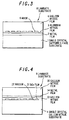
- Fig. 3 is a cross-sectional view showing still another preferred embodiment of a gallium nitride epitaxial laminate substrate to which the production process of a gallium nitride crystal substrate according to the invention has been applied.
- a single crystal sapphire C-face substrate 1 having a diameter of 50.8 mm (about 2 in.) was provided as a starting substrate, and a silver film 2 was deposited as a metal film by sputtering on the substrate to a thickness of 200 nm.
- This substrate was placed in an MOCVD furnace. In this furnace, an aluminum nitride film 3 was grown using TMA and ammonia as starting materials at a substrate temperature of 800°C on the surface of the silver film 2 to a thickness of 150 nm. Subsequently, the substrate temperature was raised to 1050°C, and a gallium nitride film was grown using TMG and ammonia as starting materials on the substrate to a thickness of 1 ⁇ m.
- An SiO 2 film 6 was deposited on the substrate by PCVD to a thickness of 0.6 ⁇ m, and stripe windows parallel to ⁇ 1-100> were formed by photolithography in the SiO 2 film to expose the gallium nitride film. The width of the windows was about 2 ⁇ m, and the width of the mask was about 8 ⁇ m.
- the laminate substrate 8 thus obtained was taken out of the HVPE furnace and was immersed in hot sulfuric acid to dissolve and remove the silver film 2, whereby the single crystal sapphire C-face substrate 1 was separated from the gallium nitride film 4.
- a single crystal free standing substrate 4 of gallium nitride was prepared.
- the surface of the single crystal substrate 4 of gallium nitride was observed by atomic force microscopy to measure the density of surface pits. As a result, the density was as low as 2 x 10 4 pits/cm 2 , confirming that the single crystal substrate of gallium nitride had high crystallinity.
- Fig. 4 is a cross-sectional view showing a further preferred embodiment of a gallium nitride epitaxial laminate substrate to which the production process of a gallium nitride crystal substrate according to the invention has been applied.
- a single crystal gallium nitride substrate 4 having a diameter of 50,8 mm (about 2 in.) produced by the method described in Example 2 was provided as a starting substrate, and an SiO 2 film 31 was deposited on the single crystal gallium nitride substrate 4 by thermal CVD to a thickness of 0.5 ⁇ m, and stripe windows 32 parallel to ⁇ 11-20> were formed by photolithography in the SiO 2 film 31 to expose the surface of the gallium nitride substrate.
- the width of the windows 32 was about 3 ⁇ m, and the width of the mask of the SiO 2 film 31 was about 7 ⁇ m.
- This substrate was placed in an MOCVD furnace. In this furnace, the substrate temperature was raised to 1050°C, and a gallium nitride film 33 was grown using TMG and ammonia as starting materials to a thickness of 2 ⁇ m.
- Gallium nitride was first selectively grown on the windows 32, and after the windows of the mask were filled with the gallium nitride, gallium nitride was laterally grown on the mask to cover the whole surface of the substrate. Finally, a gallium nitride film 33 having a flat surface was formed.
- a gold film 34 was vapor deposited as a metal film on the substrate to a thickness of 0.1 ⁇ m.
- This deposited substrate was then placed in an HVPE furnace, and gallium nitride 35 was deposited on the surface of the substrate to a thickness of 300 ⁇ m.
- ammonia and gallium chloride were used as starting materials for the growth.
- the laminate substrate 9 thus obtained was taken out of the HVPE furnace and was immersed in aqua regia overnight to dissolve and remove the gold film 34, whereby the underlying epitaxially grown gallium nitride substrate 4 could be separated from the gallium nitride film 35 epitaxially grown by HVPE.
- the surface of the single crystal substrate 35 of gallium nitride was observed by atomic force microscopy to measure the density of surface pits. As a result, the density was as low as 1 x 10 5 pits/cm 2 , confirming that the single crystal substrate 35 of gallium nitride had high crystallinity.
- the substrate having an LD structure on its p side was subjected to dry etching to form a ridge structure having a width of about 4 ⁇ m and a depth of about 0.4 ⁇ m for current constriction.
- a nickel/gold electrode was formed as a p-type ohmic electrode 18 on the top of the ridge.
- a titanium/aluminum electrode was formed as an n-type ohmic electrode 19 on the whole surface of the substrate having an LD structure on its free standing GaN substrate side.
- a highly reflective coating (not shown) of TiO 2 /SiO 2 was formed on both end faces.
- the length of the device 20 was 500 ⁇ m. This device 20 was energized.
- Fig. 5 is a cross-sectional view showing one preferred embodiment of a light emitting device using the gallium nitride crystal substrate according to the invention.
- the thickness of the metal film grown on the substrate is preferably in the range of 10 to 1000 nm.
- the reason for this is as follows.
- the thickness of the metal film is less than 10 nm, it becomes difficult for the metal film to cover the whole surface of the substrate. In this case, this renders the nucleation of gallium nitride crystal grown on the metal film uneven, resulting in deteriorated crystallinity of the gallium nitride film.
- the thickness of the metal film exceeds 1000 nm, the orientation of the metal film is disturbed, resulting in deteriorated crystallinity of the gallium nitride film grown on the metal film.
- the thickness of the metal film is less than 10 nm, the substrate cannot be separated from the gallium nitride layer without difficulty.
- the thickness of the gallium nitride film grown on the metal film is preferably not less than 50 ⁇ m. The reason for this is that, after the removal of the substrate, when the gallium nitride film is used as a free standing substrate, a thickness of the gallium nitride film of less than 50 ⁇ m leads to a lack of mechanical strength which is likely to cause cracking and is likely to cause deformation such as warpage.
- the use of the metal film as a buffer layer can significantly reduce strain derived from a difference in a lattice constant or a coefficient of thermal expansion between the substrate and gallium nitride.
- a lattice constant and a coefficient of thermal expansion of the substrate closer to gallium nitride provide better results. Accordingly, when the invention is again practiced using as the substrate the gallium nitride, free standing substrate produced according to the invention, a gallium nitride, free standing substrate having lower defect density can be provided.
- the nitride crystal, which is first grown on the aluminum film is preferably grown at a temperature of 660°C or below.
- the aluminum film is heated at a temperature of 660°C or above, aluminum is melted, leading to disturbance of the orientation. In this case, a single crystal nitride film cannot be grown on the aluminum film.
- the growth temperature of the nitride crystal, which is first grown on the metal film is preferably below the melting point of the metal.
- the gallium nitride film is preferably grown by HVPE (hydride vapor phase epitaxy), because the crystal growth rate is high and a thick film can be easily formed.
- HVPE hydrogen vapor phase epitaxy
- MOCVD metal-organics chemical vapor deposition
- a method comprising a combination of a plurality of growth methods may be used. For example, a method may be adopted wherein a part of the gallium nitride film is grown by MOCVD and the gallium nitride film is then grown to large thickness by HVPE.
- a single crystal sapphire C-face substrate or a silicon (111) substrate was used.
- a single crystal silicon carbide C-face substrate or a polycrystalline silicon carbide C-axis oriented substrate may also be used.
- germanium (Ge), GaAs, GaP, InP and the like may be used for the single crystal semiconductor substrate.
- gallium nitride grown on the metal film a single crystal, free standing substrate of a ternary compound crystal, such as aluminum gallium nitride or gallium indium nitride, may be prepared. This can also be applied to the preparation of a p-type gallium nitride substrate doped with magnesium or the like.
- An alloy film of NiAl, NiGa, CoAl, CoGa or the like may be used instead of the film of an elemental an elemental metal.
- a method may be adopted wherein an element having surfactant effect, such as silicon, is first adsorbed onto the surface of the metal film and the gallium nitride film is then grown to further reduce the defect density.
- an element having surfactant effect such as silicon
- the gallium nitride film is then grown to further reduce the defect density.
- dotted windows or checkered windows may be used instead of stripe windows.
- a method may be adopted wherein the metal film per se is patterned and gallium nitride is selectively grown on the metal film to reduce the defect density in the gallium nitride.
- the gallium nitride crystal substrate according to the invention may be used as a substrate for gallium nitride devices.
- the gallium nitride crystal substrate according to the invention is used as a substrate for laser diodes, since a good gallium nitride crystal having low defect density can be provided, a highly reliable laser diode can be realized.
- the invention can realize a process for producing, in a simple manner, a gallium nitride crystal substrate, which has low defect density and has not been significantly contaminated with impurities, and a gallium nitride crystal substrate produced by the production process.
Landscapes
- Chemical & Material Sciences (AREA)
- Engineering & Computer Science (AREA)
- Crystallography & Structural Chemistry (AREA)
- Materials Engineering (AREA)
- Metallurgy (AREA)
- Organic Chemistry (AREA)
- Chemical Kinetics & Catalysis (AREA)
- General Chemical & Material Sciences (AREA)
- Inorganic Chemistry (AREA)
- Crystals, And After-Treatments Of Crystals (AREA)
- Semiconductor Lasers (AREA)
- Led Devices (AREA)
Abstract
Description
Claims (14)
- A process for producing a gallium nitride crystal substrate, comprising the steps of:depositing a metal film on a starting substrate, which is any one of a single crystal sapphire substrate, a substrate comprising a single crystal gallium nitride film grown on a sapphire substrate, and a single crystal semiconductor substrate;depositing a gallium nitride film on the metal film to form a laminate substrate; andremoving the starting substrate from the laminate substrate with the gallium nitride film deposited thereon to prepare a free standing gallium nitride crystal substrate.
- A process for producing a gallium nitride crystal substrate, comprising the steps of:depositing a metal film on a starting substrate, which is any one of a single crystal sapphire substrate, a substrate comprising a single crystal gallium nitride film grown on a sapphire substrate, and a single crystal semiconductor substrate;forming a mask region and a gallium nitride selective growth region formed of a patterned mask material on the metal film;depositing, using the selective growth region as an origin, a gallium nitride film on the selective growth region and the mask region to form a laminate substrate; andremoving the starting substrate from the laminate substrate with the gallium nitride film deposited thereon to prepare a free standing gallium nitride crystal substrate.
- A process for producing a gallium nitride crystal substrate, comprising the steps of:depositing a metal film on a starting substrate, which is any one of a single crystal sapphire substrate, a substrate comprising a single crystal gallium nitride film grown on a sapphire substrate, and a single semiconductor crystal substrate;depositing a gallium nitride film on the metal film;forming a mask region and a gallium nitride selective growth region formed of a patterned mask material on the gallium nitride film;again depositing, using the selective growth region as an origin, a gallium nitride film on the selective growth region and the mask region to form a laminate substrate; andremoving the starting substrate from the laminate substrate with the gallium nitride film again deposited thereon to prepare a free standing gallium nitride crystal substrate.
- A process for producing a gallium nitride crystal substrate, comprising the steps of:forming a mask region and a gallium nitride selective growth region formed of a patterned mask material on a starting substrate, which is any one of a single crystal sapphire substrate, a substrate comprising a single crystal gallium nitride film grown on a sapphire substrate, and a single crystal semiconductor substrate:depositing, using the selective growth region as an origin, a gallium nitride film on the selective growth region and the mask region:forming a metal film on the gallium nitride film;again depositing a gallium nitride film on the metal film to form a laminate substrate; andremoving the starting substrate from the laminate substrate with the gallium nitride film again deposited thereon to prepare a free standing gallium nitride crystal substrate.
- The process according to any one of claims 1 to 4, which uses, as the starting substrate, the free standing gallium nitride crystal substrate produced by the process according to any one of claims 1 to 4.
- The process according to any one of claims 1 to 5, wherein the metal film is a metal film having C-axis orientation.
- The process according to any one of claims 1 to 6, wherein the metal film is formed of a member selected from the group consisting of aluminum, gold, silver, copper, platinum, iron, nickel, titanium, zirconium, and hafnium and alloys containing any one of said metals.
- The process according to any one of claims 1 to 7, wherein the metal film has a thickness in the range of 10 to 1000 nm.
- The process according to any one of claims 1 to 8, wherein the gallium nitride is deposited to a thickness of not less than 50 µm on the metal film.
- The process according to any one of claims 1 to 9, wherein aluminum nitride is deposited on the metal film and gallium nitride is deposited on the aluminum nitride.
- The process according to any one of claims 1 to 10, wherein a part or the whole of the step of depositing gallium nitride is carried out by HVPE (hydride vapor phase epitaxy).
- The process according to any one of claims 1 to 11, wherein the step of removing the starting substrate is the step of separating the gallium nitride film from the substrate through the metal film.
- The process according to claim 12, wherein the gallium nitride film is separated from the starting substrate by etching the metal film.
- A free standing gallium nitride crystal substrate obtainable by the process according to any one of claims 1 to 13.
Applications Claiming Priority (2)
| Application Number | Priority Date | Filing Date | Title |
|---|---|---|---|
| JP2001088294 | 2001-03-26 | ||
| JP2001088294A JP2002284600A (en) | 2001-03-26 | 2001-03-26 | Gallium nitride crystal substrate manufacturing method and gallium nitride crystal substrate |
Publications (2)
| Publication Number | Publication Date |
|---|---|
| EP1245702A2 true EP1245702A2 (en) | 2002-10-02 |
| EP1245702A3 EP1245702A3 (en) | 2005-06-29 |
Family
ID=18943411
Family Applications (1)
| Application Number | Title | Priority Date | Filing Date |
|---|---|---|---|
| EP02252184A Withdrawn EP1245702A3 (en) | 2001-03-26 | 2002-03-26 | Process for producing a gallium nitride crystal substrate |
Country Status (6)
| Country | Link |
|---|---|
| US (1) | US6824610B2 (en) |
| EP (1) | EP1245702A3 (en) |
| JP (1) | JP2002284600A (en) |
| KR (1) | KR100838433B1 (en) |
| CN (1) | CN1249780C (en) |
| TW (1) | TW538548B (en) |
Cited By (8)
| Publication number | Priority date | Publication date | Assignee | Title |
|---|---|---|---|---|
| FR2852974A1 (en) * | 2003-03-31 | 2004-10-01 | Soitec Silicon On Insulator | PROCESS FOR THE PRODUCTION OF MONOCRYSTALLINE CRYSTALS |
| FR2860248A1 (en) * | 2003-09-26 | 2005-04-01 | Centre Nat Rech Scient | PROCESS FOR PRODUCING AUTOMATED SUBSTRATES OF ELEMENT III NITRIDES BY HETERO-EPITAXIA ON A SACRIFICIAL LAYER |
| EP1930957A4 (en) * | 2005-09-30 | 2009-08-19 | Lattice Power Jiangxi Corp | PROCESS FOR PRODUCING ALUMINUM GALLIUM INDIUM NITRIDE THIN FILM ON A SILICON SUBSTRATE |
| EP1679740A4 (en) * | 2003-10-27 | 2009-09-02 | Sumitomo Electric Industries | GALLIUM NITRIDE SEMICONDUCTOR SUBSTRATE AND PROCESS FOR PRODUCING THE SAME |
| EP1246233A3 (en) * | 2001-03-27 | 2009-09-09 | Nec Corporation | Semiconductor substrate made of group III nitride, and process for manufacture thereof |
| EP1876270A4 (en) * | 2005-04-04 | 2009-09-23 | Tohoku Techno Arch Co Ltd | METHOD FOR DRAWING GAN MONOCRYSTAL, METHOD FOR PREPARING GAN SUBSTRATE, METHOD FOR MANUFACTURING GAN-BASED ELEMENT, AND GAN-BASED ELEMENT |
| WO2012007350A1 (en) * | 2010-07-15 | 2012-01-19 | Osram Opto Semiconductors Gmbh | Semiconductor component, substrate and method for producing a semiconductor layer sequence |
| FR3112238A1 (en) | 2020-07-06 | 2022-01-07 | Saint-Gobain Lumilog | SEMICONDUCTOR SUBSTRATE WITH NITRURED INTERFACE LAYER |
Families Citing this family (56)
| Publication number | Priority date | Publication date | Assignee | Title |
|---|---|---|---|---|
| JP2004107114A (en) * | 2002-09-17 | 2004-04-08 | Toyoda Gosei Co Ltd | Method of manufacturing group iii nitride compound semiconductor substrate |
| JP4545389B2 (en) * | 2003-03-26 | 2010-09-15 | 日本碍子株式会社 | Dislocation reduction method for epitaxial substrate and group III nitride layer group |
| US6825123B2 (en) * | 2003-04-15 | 2004-11-30 | Saint-Goban Ceramics & Plastics, Inc. | Method for treating semiconductor processing components and components formed thereby |
| JP4457576B2 (en) | 2003-05-08 | 2010-04-28 | 住友電気工業株式会社 | Group III-V compound crystal and method for producing the same |
| JP4390640B2 (en) * | 2003-07-31 | 2009-12-24 | シャープ株式会社 | Nitride semiconductor laser device, nitride semiconductor light emitting device, nitride semiconductor wafer, and methods of manufacturing the same |
| CN100453712C (en) * | 2003-08-28 | 2009-01-21 | 日立电线株式会社 | III-V nitride-based semiconductor substrate and manufacturing method thereof |
| TWI234298B (en) * | 2003-11-18 | 2005-06-11 | Itswell Co Ltd | Semiconductor light emitting diode and method for manufacturing the same |
| KR100613273B1 (en) * | 2003-12-30 | 2006-08-18 | 주식회사 이츠웰 | Light emitting diodes and manufacturing method thereof |
| KR101094403B1 (en) * | 2004-01-29 | 2011-12-15 | 삼성코닝정밀소재 주식회사 | Reduced warpage of sapphire / gallium nitride laminates |
| WO2005074048A1 (en) * | 2004-01-31 | 2005-08-11 | Itswell Co. Ltd. | Free-standing semiconductor substrate and the manufacturing method and manufacturing apparatus thereof |
| US8174037B2 (en) | 2004-09-22 | 2012-05-08 | Cree, Inc. | High efficiency group III nitride LED with lenticular surface |
| KR100728533B1 (en) * | 2004-11-23 | 2007-06-15 | 삼성코닝 주식회사 | Gallium nitride single crystal thick film and method for manufacturing same |
| EP1681712A1 (en) | 2005-01-13 | 2006-07-19 | S.O.I. Tec Silicon on Insulator Technologies S.A. | Method of producing substrates for optoelectronic applications |
| DE102005003884A1 (en) * | 2005-01-24 | 2006-08-03 | Forschungsverbund Berlin E.V. | Process for the preparation of c-plane oriented GaN or AlxGa1-xN substrates |
| JP4817673B2 (en) * | 2005-02-25 | 2011-11-16 | 三洋電機株式会社 | Nitride semiconductor device fabrication method |
| GB0509328D0 (en) * | 2005-05-09 | 2005-06-15 | Univ Nottingham | A bulk, free-standing cubic III-N substrate and a method for forming same |
| CN100561669C (en) * | 2005-05-16 | 2009-11-18 | 中国科学院合肥物质科学研究院 | Preparation method of gallium nitride thin film material |
| KR20060131327A (en) * | 2005-06-16 | 2006-12-20 | 엘지전자 주식회사 | Manufacturing method of light emitting diode |
| KR100638869B1 (en) * | 2005-06-21 | 2006-10-27 | 삼성전기주식회사 | A method of forming a nitride compound layer and a method of manufacturing a BAN substrate and a vertical structure nitride semiconductor light emitting device using the same |
| JP2007134388A (en) * | 2005-11-08 | 2007-05-31 | Sharp Corp | Nitride-based semiconductor device and manufacturing method thereof |
| EP1960571A2 (en) * | 2005-11-17 | 2008-08-27 | Mosaic Crystals Ltd. | Gan crystal sheet |
| JP5131889B2 (en) * | 2005-12-06 | 2013-01-30 | 学校法人 名城大学 | Method of manufacturing nitride compound semiconductor device |
| US20070138505A1 (en) | 2005-12-12 | 2007-06-21 | Kyma Technologies, Inc. | Low defect group III nitride films useful for electronic and optoelectronic devices and methods for making the same |
| WO2007072984A1 (en) * | 2005-12-20 | 2007-06-28 | Tohoku Techno Arch Co., Ltd. | Semiconductor substrate manufacturing method and element structure manufacturing method |
| US9406505B2 (en) * | 2006-02-23 | 2016-08-02 | Allos Semiconductors Gmbh | Nitride semiconductor component and process for its production |
| KR100813561B1 (en) * | 2006-03-14 | 2008-03-17 | 주식회사 이츠웰 | Semiconductor substrate and manufacturing method thereof |
| JP4860309B2 (en) * | 2006-03-17 | 2012-01-25 | 日本碍子株式会社 | Group III nitride crystal manufacturing apparatus and group III nitride crystal multilayer structure manufacturing method |
| WO2007122669A1 (en) * | 2006-03-29 | 2007-11-01 | Fujitsu Limited | COMPOUND SEMICONDUCTOR WAFER HAVING POLYCRYSTALLINE SiC SUBSTRATE, COMPOUND SEMICONDUCTOR DEVICE, AND PROCESSES FOR PRODUCING THESE |
| JP4873381B2 (en) * | 2006-03-31 | 2012-02-08 | 信越半導体株式会社 | Light emitting device manufacturing method, compound semiconductor wafer, and light emitting device |
| JP4997502B2 (en) * | 2006-09-20 | 2012-08-08 | 国立大学法人東北大学 | Manufacturing method of semiconductor device |
| JP4852755B2 (en) * | 2006-09-20 | 2012-01-11 | 国立大学法人東北大学 | Method for manufacturing compound semiconductor device |
| KR100843474B1 (en) * | 2006-12-21 | 2008-07-03 | 삼성전기주식회사 | Group III nitride single crystal growth method and nitride single crystal prepared using the same |
| CN101221898B (en) * | 2007-01-08 | 2011-05-11 | 晶能光电(江西)有限公司 | Method for manufacturing metallic substrate with high quality surface |
| US7749325B2 (en) | 2007-01-22 | 2010-07-06 | Sumitomo Electric Industries, Ltd. | Method of producing gallium nitride (GaN) independent substrate, method of producing GaN crystal body, and method of producing GaN substrate |
| JP4877241B2 (en) * | 2008-02-01 | 2012-02-15 | 豊田合成株式会社 | Method for producing group III nitride compound semiconductor substrate |
| JP5075692B2 (en) * | 2008-03-18 | 2012-11-21 | 古河機械金属株式会社 | Group III nitride semiconductor substrate forming substrate |
| JP5014217B2 (en) * | 2008-03-18 | 2012-08-29 | Dowaエレクトロニクス株式会社 | Group III nitride semiconductor and method of manufacturing the same |
| JP5684551B2 (en) * | 2008-12-26 | 2015-03-11 | Dowaホールディングス株式会社 | Group III nitride semiconductor growth substrate, group III nitride semiconductor epitaxial substrate, group III nitride semiconductor device, group III nitride semiconductor free-standing substrate, and methods of manufacturing the same |
| CN102326228B (en) * | 2008-12-26 | 2014-03-05 | 同和控股(集团)有限公司 | III-nitride semiconductor growth substrate, III-nitride semiconductor epitaxial substrate, III-nitride semiconductor element, III-nitride semiconductor freestanding substrate, and method for fabricating these |
| MY158571A (en) | 2009-03-13 | 2016-10-14 | Saint Gobain Ceramics | Chemical mechanical planarization using nanodiamond |
| WO2011066029A2 (en) * | 2009-09-10 | 2011-06-03 | The Regents Of The University Of Michigan | Methods of preparing flexible photovoltaic devices using epitaxial liftoff, and preserving the integrity of growth substrates used in epitaxial growth |
| JP5515770B2 (en) * | 2009-09-14 | 2014-06-11 | 住友電気工業株式会社 | Method of forming nitride semiconductor epitaxial layer and method of manufacturing nitride semiconductor device |
| JP5741042B2 (en) * | 2011-02-14 | 2015-07-01 | 富士通株式会社 | Compound semiconductor device and manufacturing method thereof |
| US9312436B2 (en) | 2011-05-16 | 2016-04-12 | Kabushiki Kaisha Toshiba | Nitride semiconductor device, nitride semiconductor wafer, and method for manufacturing nitride semiconductor layer |
| US20120292648A1 (en) * | 2011-05-16 | 2012-11-22 | Kabushiki Kaisha Toshiba | Nitride semiconductor device, nitride semiconductor wafer, and method for manufacturing nitride semiconductor layer |
| JP5551131B2 (en) * | 2011-09-14 | 2014-07-16 | 株式会社東芝 | Manufacturing method of nitride semiconductor multilayer structure |
| US9236271B2 (en) * | 2012-04-18 | 2016-01-12 | Globalfoundries Inc. | Laser-initiated exfoliation of group III-nitride films and applications for layer transfer and patterning |
| JPWO2013176291A1 (en) * | 2012-05-23 | 2016-01-14 | 日本碍子株式会社 | Composite substrate, light emitting device, and method of manufacturing composite substrate |
| US9252324B2 (en) | 2013-05-30 | 2016-02-02 | Globalfoundries Inc | Heterojunction light emitting diode |
| CN103996607B (en) * | 2014-05-30 | 2016-10-19 | 广州市众拓光电科技有限公司 | Growth metal Al monocrystal thin films on a sapphire substrate and its preparation method and application |
| EP3298181A1 (en) * | 2015-05-21 | 2018-03-28 | EV Group E. Thallner GmbH | Method for applying an overgrowth layer onto a seed layer |
| CN109715751A (en) | 2016-09-23 | 2019-05-03 | 圣戈本陶瓷及塑料股份有限公司 | Chemical-mechanical planarization sizing agent and forming method thereof |
| KR102742153B1 (en) * | 2016-10-21 | 2024-12-12 | 삼성전자주식회사 | Methods of manufacturing a gallium nitride substrate |
| KR102849602B1 (en) * | 2019-09-30 | 2025-08-21 | 가부시키가이샤 플로스피아 | Laminated structures and semiconductor devices |
| CN113078046B (en) * | 2021-03-26 | 2022-07-29 | 华厦半导体(深圳)有限公司 | Gallium nitride homogeneous substrate and preparation method thereof |
| CN114059036B (en) * | 2021-11-23 | 2023-03-14 | 南京大学 | Application of iron film in auxiliary stripping of diamond polycrystalline film |
Family Cites Families (9)
| Publication number | Priority date | Publication date | Assignee | Title |
|---|---|---|---|---|
| JPS63188983A (en) | 1987-01-31 | 1988-08-04 | Ricoh Co Ltd | semiconductor light emitting device |
| JP3139445B2 (en) | 1997-03-13 | 2001-02-26 | 日本電気株式会社 | GaN-based semiconductor growth method and GaN-based semiconductor film |
| JP3788037B2 (en) | 1998-06-18 | 2006-06-21 | 住友電気工業株式会社 | GaN single crystal substrate |
| US6218280B1 (en) * | 1998-06-18 | 2001-04-17 | University Of Florida | Method and apparatus for producing group-III nitrides |
| GB9916549D0 (en) * | 1999-07-14 | 1999-09-15 | Arima Optoelectronics Corp | Epitaxial growth method of semiconductors on highly lattice mismatched substrates using the buffer layer with solid-liquid phase transition |
| US6563144B2 (en) * | 1999-09-01 | 2003-05-13 | The Regents Of The University Of California | Process for growing epitaxial gallium nitride and composite wafers |
| EP1307903A1 (en) * | 2000-08-04 | 2003-05-07 | The Regents Of The University Of California | Method of controlling stress in gallium nitride films deposited on substrates |
| US6649494B2 (en) * | 2001-01-29 | 2003-11-18 | Matsushita Electric Industrial Co., Ltd. | Manufacturing method of compound semiconductor wafer |
| EP1244139A2 (en) * | 2001-03-23 | 2002-09-25 | Matsushita Electric Industrial Co., Ltd. | Manufacturing method of semiconductor film |
-
2001
- 2001-03-26 JP JP2001088294A patent/JP2002284600A/en active Pending
-
2002
- 2002-03-26 US US10/106,693 patent/US6824610B2/en not_active Expired - Lifetime
- 2002-03-26 TW TW091105958A patent/TW538548B/en not_active IP Right Cessation
- 2002-03-26 CN CNB021078866A patent/CN1249780C/en not_active Expired - Fee Related
- 2002-03-26 KR KR1020020016387A patent/KR100838433B1/en not_active Expired - Fee Related
- 2002-03-26 EP EP02252184A patent/EP1245702A3/en not_active Withdrawn
Cited By (19)
| Publication number | Priority date | Publication date | Assignee | Title |
|---|---|---|---|---|
| EP1246233A3 (en) * | 2001-03-27 | 2009-09-09 | Nec Corporation | Semiconductor substrate made of group III nitride, and process for manufacture thereof |
| FR2852974A1 (en) * | 2003-03-31 | 2004-10-01 | Soitec Silicon On Insulator | PROCESS FOR THE PRODUCTION OF MONOCRYSTALLINE CRYSTALS |
| WO2004090201A3 (en) * | 2003-03-31 | 2004-11-18 | Soitec Silicon On Insulator | Method for the production of monocrystalline crystals |
| US7282381B2 (en) | 2003-09-26 | 2007-10-16 | Centre National De La Recherche Scientifique (Cnrs) | Method of producing self supporting substrates comprising III-nitrides by means of heteroepitaxy on a sacrificial layer |
| FR2860248A1 (en) * | 2003-09-26 | 2005-04-01 | Centre Nat Rech Scient | PROCESS FOR PRODUCING AUTOMATED SUBSTRATES OF ELEMENT III NITRIDES BY HETERO-EPITAXIA ON A SACRIFICIAL LAYER |
| CN100387760C (en) * | 2003-09-26 | 2008-05-14 | 国家科学研究中心 | Method for producing self-supporting substrates comprising III nitrides by heteroepitaxy on sacrificial layers |
| WO2005031045A3 (en) * | 2003-09-26 | 2005-05-26 | Centre Nat Rech Scient | Method of producing self-supporting substrates comprising iii-nitrides by means of heteroepitaxy on a sacrificial layer |
| EP1679740A4 (en) * | 2003-10-27 | 2009-09-02 | Sumitomo Electric Industries | GALLIUM NITRIDE SEMICONDUCTOR SUBSTRATE AND PROCESS FOR PRODUCING THE SAME |
| EP2197050A1 (en) * | 2005-04-04 | 2010-06-16 | Tohoku Techno Arch Co., Ltd. | Process for producing a GaN-based element |
| EP1876270A4 (en) * | 2005-04-04 | 2009-09-23 | Tohoku Techno Arch Co Ltd | METHOD FOR DRAWING GAN MONOCRYSTAL, METHOD FOR PREPARING GAN SUBSTRATE, METHOD FOR MANUFACTURING GAN-BASED ELEMENT, AND GAN-BASED ELEMENT |
| EP2197049A1 (en) * | 2005-04-04 | 2010-06-16 | Tohoku Techno Arch Co., Ltd. | Process for producing a GaN-based element |
| EP2219236A1 (en) * | 2005-04-04 | 2010-08-18 | Tohoku Techno Arch Co., Ltd. | Process for producing a GaN-based element |
| US7829435B2 (en) | 2005-04-04 | 2010-11-09 | Tohoku Techno Arch Co., Ltd. | Method for growth of GaN single crystal, method for preparation of GaN substrate, process for producing GaN-based element, and GaN-based element |
| US8124504B2 (en) | 2005-04-04 | 2012-02-28 | Tohoku Techno Arch Co., Ltd. | Method for growth of GaN single crystal, method for preparation of GaN substrate, process for producing GaN-based element, and GaN-based element |
| EP1930957A4 (en) * | 2005-09-30 | 2009-08-19 | Lattice Power Jiangxi Corp | PROCESS FOR PRODUCING ALUMINUM GALLIUM INDIUM NITRIDE THIN FILM ON A SILICON SUBSTRATE |
| WO2012007350A1 (en) * | 2010-07-15 | 2012-01-19 | Osram Opto Semiconductors Gmbh | Semiconductor component, substrate and method for producing a semiconductor layer sequence |
| FR3112238A1 (en) | 2020-07-06 | 2022-01-07 | Saint-Gobain Lumilog | SEMICONDUCTOR SUBSTRATE WITH NITRURED INTERFACE LAYER |
| WO2022008836A1 (en) | 2020-07-06 | 2022-01-13 | Saint-Gobain Lumilog | Semiconductor substrate with nitrided interface layer |
| US12506003B2 (en) | 2020-07-06 | 2025-12-23 | Ivworks Co., Ltd. | Semiconductor substrate with nitride interface layer |
Also Published As
| Publication number | Publication date |
|---|---|
| CN1249780C (en) | 2006-04-05 |
| TW538548B (en) | 2003-06-21 |
| EP1245702A3 (en) | 2005-06-29 |
| KR100838433B1 (en) | 2008-06-16 |
| US6824610B2 (en) | 2004-11-30 |
| JP2002284600A (en) | 2002-10-03 |
| US20020175340A1 (en) | 2002-11-28 |
| KR20020076167A (en) | 2002-10-09 |
| CN1378238A (en) | 2002-11-06 |
Similar Documents
| Publication | Publication Date | Title |
|---|---|---|
| US6824610B2 (en) | Process for producing gallium nitride crystal substrate, and gallium nitride crystal substrate | |
| KR100401898B1 (en) | Base substrate for crystal growth and manufacturing method of substrate by using the same | |
| JP3139445B2 (en) | GaN-based semiconductor growth method and GaN-based semiconductor film | |
| EP1041610B1 (en) | GaN SINGLE CRYSTALLINE SUBSTRATE AND METHOD OF PRODUCING THE SAME | |
| US7674699B2 (en) | III group nitride semiconductor substrate, substrate for group III nitride semiconductor device, and fabrication methods thereof | |
| JP5361107B2 (en) | Method for improving the epitaxy quality (surface roughness and defect density) of aluminum nitride, indium, gallium ((Al, In, Ga) N) free-standing substrates for optoelectronic devices and electronics devices | |
| US6924159B2 (en) | Semiconductor substrate made of group III nitride, and process for manufacture thereof | |
| CN101060102B (en) | Nitride semiconductor substrate, manufacturing method thereof, and epitaxial substrate for nitride semiconductor light-emitting device | |
| US20070176199A1 (en) | Nitride-based group III-V semiconductor substrate and fabrication method therefor, and nitride-based group III-V light-emitting device | |
| WO2010025153A1 (en) | Nitride crystal with removable surface layer and methods of manufacture | |
| JP2008277841A (en) | Method for manufacturing group III-V nitride semiconductor substrate | |
| JP5638198B2 (en) | Laser diode orientation on miscut substrates | |
| JP4734786B2 (en) | Gallium nitride compound semiconductor substrate and manufacturing method thereof | |
| EP1709670B1 (en) | Group iii nitride semiconductor multilayer structure | |
| JP2000223417A (en) | Semiconductor growing method, semiconductor substrate manufacturing method, and semiconductor device manufacturing method | |
| JP2007246331A (en) | III-V nitride semiconductor substrate and method for manufacturing the same | |
| KR100586940B1 (en) | Method of manufacturing gallium nitride based single crystal substrate | |
| US6339014B1 (en) | Method for growing nitride compound semiconductor | |
| JPH1179897A (en) | Crystal growth method of gallium nitride thick film | |
| JP2009023853A (en) | III-V nitride semiconductor substrate, method of manufacturing the same, and III-V nitride semiconductor device | |
| JP2001148348A (en) | Gab SEMICONDUCTOR ELEMENT AND MANUFACTURING METHOD | |
| Bessolov et al. | Semipolar Wide-Band III–N-Layers on a Silicon Substrate: Orientation Controlling Epitaxy and the Properties of Structures | |
| JP2000277440A (en) | Nitride III-V compound semiconductor crystal film, semiconductor device using nitride III-V compound semiconductor crystal film, and semiconductor laser using nitride III-V compound semiconductor crystal film | |
| JP4186076B2 (en) | Manufacturing method of nitride semiconductor substrate | |
| JP2003243776A (en) | Support substrate peeling method |
Legal Events
| Date | Code | Title | Description |
|---|---|---|---|
| PUAI | Public reference made under article 153(3) epc to a published international application that has entered the european phase |
Free format text: ORIGINAL CODE: 0009012 |
|
| AK | Designated contracting states |
Kind code of ref document: A2 Designated state(s): AT BE CH CY DE DK ES FI FR GB GR IE IT LI LU MC NL PT SE TR |
|
| AX | Request for extension of the european patent |
Free format text: AL;LT;LV;MK;RO;SI |
|
| PUAL | Search report despatched |
Free format text: ORIGINAL CODE: 0009013 |
|
| AK | Designated contracting states |
Kind code of ref document: A3 Designated state(s): AT BE CH CY DE DK ES FI FR GB GR IE IT LI LU MC NL PT SE TR |
|
| AX | Request for extension of the european patent |
Extension state: AL LT LV MK RO SI |
|
| RIC1 | Information provided on ipc code assigned before grant |
Ipc: 7H 01L 21/20 B Ipc: 7C 30B 25/18 B Ipc: 7C 30B 29/40 A |
|
| RAP1 | Party data changed (applicant data changed or rights of an application transferred) |
Owner name: HITACHI CABLE, LTD. |
|
| 17P | Request for examination filed |
Effective date: 20051213 |
|
| AKX | Designation fees paid |
Designated state(s): FR GB |
|
| REG | Reference to a national code |
Ref country code: DE Ref legal event code: 8566 |
|
| STAA | Information on the status of an ep patent application or granted ep patent |
Free format text: STATUS: THE APPLICATION HAS BEEN WITHDRAWN |
|
| 18W | Application withdrawn |
Effective date: 20130820 |