EP1249706A2 - Non-contact voltage measurement method and device, and related detection probe - Google Patents
Non-contact voltage measurement method and device, and related detection probe Download PDFInfo
- Publication number
- EP1249706A2 EP1249706A2 EP02252419A EP02252419A EP1249706A2 EP 1249706 A2 EP1249706 A2 EP 1249706A2 EP 02252419 A EP02252419 A EP 02252419A EP 02252419 A EP02252419 A EP 02252419A EP 1249706 A2 EP1249706 A2 EP 1249706A2
- Authority
- EP
- European Patent Office
- Prior art keywords
- conductor
- detection electrode
- detection
- electrode
- measuring
- Prior art date
- Legal status (The legal status is an assumption and is not a legal conclusion. Google has not performed a legal analysis and makes no representation as to the accuracy of the status listed.)
- Granted
Links
Images


Classifications
-
- G—PHYSICS
- G01—MEASURING; TESTING
- G01R—MEASURING ELECTRIC VARIABLES; MEASURING MAGNETIC VARIABLES
- G01R15/00—Details of measuring arrangements of the types provided for in groups G01R17/00 - G01R29/00, G01R33/00 - G01R33/26 or G01R35/00
- G01R15/14—Adaptations providing voltage or current isolation, e.g. for high-voltage or high-current networks
- G01R15/16—Adaptations providing voltage or current isolation, e.g. for high-voltage or high-current networks using capacitive devices
-
- G—PHYSICS
- G01—MEASURING; TESTING
- G01R—MEASURING ELECTRIC VARIABLES; MEASURING MAGNETIC VARIABLES
- G01R31/00—Arrangements for testing electric properties; Arrangements for locating electric faults; Arrangements for electrical testing characterised by what is being tested not provided for elsewhere
- G01R31/28—Testing of electronic circuits, e.g. by signal tracer
- G01R31/302—Contactless testing
- G01R31/312—Contactless testing by capacitive methods
Definitions
- the present invention relates to a detection probe respectively used in a method and a device for measuring an AC voltage applied to a conductor insulated by insulation, such as a vinyl insulated electrical wire, without contacting the conductor.
- an AC voltmeter is generally used in the measurement of a voltage of a commercial AC current (supply) being applied to an insulated electrical wire.
- Fig. 13 is a block diagram showing the structure of a non-contact voltage measurement device 80 of the related art
- Fig. 14 is an equivalent circuit of essential parts of the voltage measurement device 80.
- the voltage measurement device 80 comprises a detection resistor R1, a detection probe 11, an oscillator 12, a current detection section 13j, a band pass filter 21, a rectifier 22, a capacitance calculation section 23, a floating capacitance detection section 24, a switch 25, a low pass filter 26, an integrator 27 and a divider 28.
- the detection probe 11 is provided with a detection electrode 111 for electrostatically shielding part of a conductor CD, by covering part of the surface of insulation SL of an electrical wire WR from the outside, and a shield electrode 112 for electrostatically shielding the detection electrode 111 from the outside.
- Impedance Zw between the detection electrode 111 and the conductor CD is measured using the detection probe 11.
- reactance XC1 namely capacitance C1 is measured in place of the impedance Zw.
- Capacitance C0 is sometimes referred to as "floating capacitance C0"
- Electric current flowing from the oscillator 12 through the detection resistor R1 into the detection electrode 111 is Is, and electric current discharged from the detection electrode 111 towards the oscillator 12 is Ix.
- Is Electric current flowing from the oscillator 12 through the detection resistor R1 into the detection electrode 111
- Ix electric current discharged from the detection electrode 111 towards the oscillator 12
- Is 0 flowing through the floating capacitance C0 to a ground terminal
- a current Is 1 flowing through the capacitance C1 and the conductor CD to the ground terminal.
- the oscillator 12 outputs, for example, a 5KHz sine wave signal of a certain voltage Es.
- the current detection section 13j detects current flowing into the detection electrode 111 and current discharged from the detection electrode 111, and outputs a signal S1.
- the band pass filter 21 allows only a component due to the signal Es of the oscillator 12 to pass.
- the floating capacitance detection section 24 measures and stores floating capacitance C0 with the detection probe 11 separated from the electrical wire WR.
- the capacitance calculation section 23 calculates capacitance C1 based on a signal S3 output from the rectifier 22 with the surface of the insulation SL covered by the detection probe 11, and the floating capacitance C0 stored in the floating capacitance detection section 24.
- the obtained capacitance C1 is output to the divider 28 as a signal S4.
- the low pass filter 26 allows only a component due to the voltage Ex applied to the conductor CD to pass.
- the integrator 27 integrates a signal S5 output from the low pass filter 26. In this way, phase compensation of the signal waveform is carried out.
- the divider 28 obtains a voltage Ex by dividing the signal S6 (Erx) output from the integrator 27 by the signal S4 (capacitance C1) output from the capacitance calculation section 23.
- the floating capacitance C0 is measured with the detection probe 11 in an open state.
- a value of floating capacitance Co obtained from this equation (3) is stored in the floating capacitance detection section 24. Next, capacitance C1 is measured with the detection probe 11 closed.
- a value of capacitance (C0 + C1) obtained from this equation (7) is input to the capacitance calculation section 23 as a signal S3.
- capacitance C1 is obtained by subtracting the value of floating capacitance C0 stored in the floating capacitance detection section 24 from the input value of capacitance (C0 + C1), and this is output to the divider 28.
- a voltage Er developed across the two ends of the detection resistor R1 by this current is:
- a value of voltage Er (Ers) obtained from this equation (10) is input to the divider 28 as a signal S6.
- the floating capacitance C0 is not fixed and varies depending on the diameter of the conductor CD, conditions of fitting conductor CD to the detection probe 11, conditions surrounding the detection probe 11 etc. Measurement errors arise because of variations in the floating capacitance C0. Overall measurement accuracy is also affected by floating capacitance C0 measurement errors.
- An object of the present invention is to provide a non-contact measurement method and device, and a detection probe used with this method and device, that is not affected by floating capacitance, and that can measure a voltage in a non-contact manner through a simple operation and without measuring floating capacitance.
- an imaginary short-circuit is established by connecting the core wire and the sheath wire to an inverting input terminal and a non-inverting input terminal of an operational amplifier, and a voltage applied to the conductor is obtained by applying the signal from the oscillator to the detection electrode via the shield cable to measure impedance between the detection electrode and the conductor.
- a device of one aspect of the present invention comprises a detection probe, provided with a detection electrode capable of electrostatically shielding part of the conductor by covering part of the surface of the insulation from the outside, and a shield electrode for electrostaticaly shielding the detection electrode from the outside, a shield cable, having one end of a core wire and a sheath wire connected to the detection electrode and the shield electrode, an operational amplifier for, with respect to other ends of the shield cable, establishing an imaginary short circuit condition by connecting the core wire and the sheath wire to an inverting input terminal and a non-inverting input terminal, an oscillator for outputting a signal having a certain frequency, and a measurement section, for applying the signal from the oscillator to the detection electrode via the shield cable to measure impedance between the detection electrode and the conductor, and obtaining the voltage applied to the conductor based on the measured results.
- a device of another aspect of the present invention comprises an oscillator for applying a signal having a certain frequency to the detection electrode via the shield cable, a detection resistor, for detecting current discharged from the detection electrode attributable to the signal, and detecting current discharged from the detection electrode attributable to a voltage applied to the conductor, and a measurement section for obtaining the voltage applied to the conductor based on a voltage developed across the two ends of the detection resistor.
- correction circuit for correcting an error of the operational amplifier so that the imaginary short-circuit state is made close to perfect.
- an inverting amplifier having the signal input to an input terminal, and one end of the detection resistor connected to an output terminal, and forming a feedback circuit by way of an inverting input terminal and a non-inverting input terminal of the operational amplifier.
- a current detection transformer provided stretching across a housing and a cover so as to be capable of opening and closing together with opening and closing of the cover.
- a detection probe of one aspect of the present invention comprises a housing, a cover capable of being opened and closed with respect to the housing, a detection electrode, provided stretching across the housing and the cover so as to be capable of opening and closing together with opening and closing of the cover, having a movable section that can be pressed by applying force towards the insulation, and being capable of covering a surface of part of the insulation, and a shield electrode for covering the detection electrode, provided stretching across the housing and the cover so as to be capable of opening and closing together with opening and closing of the cover.
- Fig. 1 is a block diagram showing the structure of a voltage measurement device 1 of the first embodiment of the present invention
- Fig. 2 is a block diagram showing an example structure of a measurement section 30
- Fig. 3 is a block diagram showing another example structure of a measurement section 30B
- Fig. 4 is an equivalent circuit of essential parts of the voltage measurement device 1.
- the voltage measurement device 1 comprises a detection probe 11, a coaxial cable (shield cable) CV, an oscillator 12, a current detector 13 and a measurement section 30.
- the detection probe 11 is provided with a detection electrode 111 electrostatically shielding part of a conductor CD by covering part of a surface of insulation SL of an electrical wire WR from the outside, and a shield probe 112 electrostatically shielding the detection electrode 111 from the outside.
- the detection probe 11 and the current detection section 13 are connected by the coaxial cable CV. At that time, the detection electrode 111 is connected to a core wire of one side of the coaxial cable CV and the shield electrode 112 is connected to a sheath wire at the same side.
- the oscillator 12 outputs a sine wave signal having a frequency that is sufficiently higher than a commercial power supply frequency of 50 HZ or 60 Hz, for example 2 KHz or 5 KHz, and has a certain voltage Es.
- the current detection section 13 comprises operational amplifiers Q1 - Q3, a detection resistor R1 and resistors R2 - R7.
- the operational amplifier Q1 forms an inverting amplifier circuit K1.
- the output terminal and the inverting input terminal a of the operational amplifier Q2 are connected together, and this operational amplifier Q2 constitutes a voltage follower circuit K2.
- the operational amplifier Q3 forms a differential amplifier circuit K3.
- the sheath wire of the coaxial cable CV is connected to the inverting input terminal a of the operational amplifier Q2, while the core wire of the coaxial cable CV is connected to the non-inverting input terminal b .
- the inverting input terminal a and the non-inverting input terminal b are at substantially the same potential, that is, they are in an imaginary short-circuit state.
- Impedance Zw between the detection electrode 111 and the conductor CD is measured using the detection probe 11.
- reactance XC between the detection electrode 111 and the conductor CD, namely capacitance C, is measured instead of impedance Zw.
- Reactance XC is different depending on the frequency f, even if the capacitance C is fixed, and so reactance for frequency fs of the voltage Es from the oscillator 12 will be termed XCs, and reactance for frequency fx of the voltage Ex applied to the conductor CD will be termed XCx.
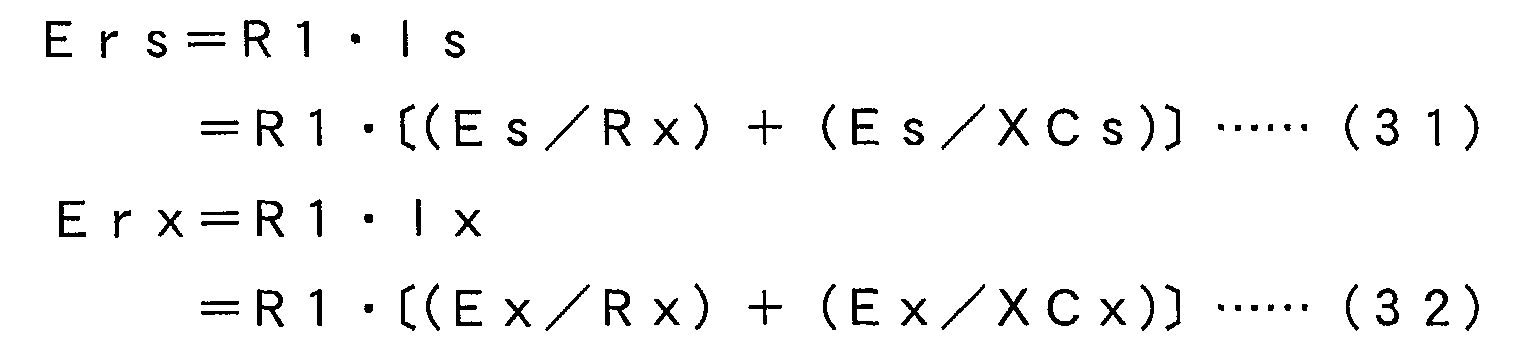
- the voltage Er developed across the two ends of the detection resistor R1 includes a component Erx due to current Ix attributable to the voltage Ex of the conductor CD, and a component Ers due to current Is attributable to the voltage Es output from the oscillator 12. These voltage components Ers and Erx are discriminated using a filter or the like by utilizing characteristics due to the fact that they have different frequencies.
- these voltage components Erx and Ers are obtained separately, impedance between the detection electrode 111 and the conductor CD is obtained, and current Ix attributable to the voltage Ex of the conductor CD is measured, and from these values the voltage Ex applied to the conductor CD is measured.
- the capacitance is measured as the impedance, but it is also possible to separately measure capacitance C (or reactance XC) and leakage resistance Rx, and to use the measurement results for calculation, as will be described later.
- Eo (V s) - V s • R 1 / j X C s
- E o (E x) E x • R 1 / j X C x
- the measurement section 30 comprises an impedance measurement section 14, a discharge current measurement section 15, a conductor voltage measurement section 16, a power measurement section 17 and a display section 18. These sections can be realized by executing a suitable computer program, using a microprocessor, ROM, RAM, etc.
- the impedance measurement section 14 measures the impedance Zw between the detection electrode 111 and the conductor CD. With this embodiment, only the capacitance C or the reactance XC is measured, for the purpose of simplification.
- the discharge current measurement section 15 measures current Ix attributable to the voltage Ex.
- the conductor voltage measurement section 16 measures voltage Ex from the current Ix and the impedance Zw.
- the power measurement section 17 measures power supplied to a load by the conductor CD based on the measured voltage Ex and input current Iw input separately. The current Iw can be detected by clamping the electrical wire WR using a current detection transformer.
- the display section 18 displays the measured voltage Ex or power.
- a measurement section 30B comprises a band pass filter 21, a rectifier 22, a low pass filter 26, a divider 28, a power measurement section 17 and a display section 18.
- the band pass filter 21 allows only a component due to the signal Es of the oscillator 12 to pass. Based on this, the impedance Zw (reactance XCs or reactance XCx) between the detection electrode 111 and the conductor CD is obtained.
- the low pass filter 26 allows only a component due to the voltage Ex applied to the conductor CD to pass. Based on this, current Ix attributable to voltage Ex is obtained.
- the divider 28 performs division to obtain voltage Ex.
- Fig. 5 and Fig. 6 are drawings showing examples of correction circuits 40 and 40B
- Fig. 7 is a drawing showing an example of a protection circuit.
- the correction circuit 40 shown in Fig. 5 is a phase inversion type circuit using an operational amplifier Q4. Amplitude adjustment is carried out by the resistor 41, and phase adjustment is carried out by the resistor R42.
- the correction circuit 40B shown in Fig. 6 is a phase non-inversion type circuit using an operational amplifier Q5. Amplitude adjustment is carried out by the resistor 43, and phase adjustment is carried out by the resistor R44.
- the phase non-inversion type correction circuit 40B is inserted between the output of the operational amplifier Q1 and the resistor R6. Also, the phase inversion type correction circuit 40 is inserted at the same position, the other end of the resistor R6 is connected to the inverting input terminal of the operational amplifier Q3, and the operational amplifier Q3 is made to operate as an inverting amplifier circuit.
- the sheath wire of the coaxial cable CV is connected to the inverting input terminal a of the operational amplifier Q2, but the inverting input terminal a is removed, the phase inversion type correction circuit 40B is inserted between the inverting input terminal a of the operational amplifier Q2 and the sheath wire of the coaxial cable CV, and a corrected voltage is applied to the sheath wire of the coaxial cable CV from the output terminal of the operational amplifier Q2.
- two diodes are connected in parallel in opposite directions between the inverting input terminal a and the non-inverting terminal b of the operational amplifier Q2.
- a power source is then connected to the output terminal through the diodes.
- various probes can be used as the detection probe 11.
- the detection probe disclosed in the specification of the above mentioned Japanese Patent No. 3158063 it is possible to use the detection probe 11B described in the following.
- Fig. 8 is a cross-sectional front elevation showing an example of a detection probe 11B
- Fig. 9 is a cross-sectional side elevation of the detection probe 11B.
- the detection probe 11B comprises a housing 51, a cover 52, a detection electrode 53, a shield electrode 54, a coil spring 55 and a current detection transformer 56.
- the housing 51 is made of synthetic resin having good insulating properties, and has a substantially rectangular parallelepiped shape.
- the cover 52 is also made of synthetic resin, and is attached to the housing using a hinge 57 so as to be capable of opening and closing. Openings 51a for passing an electrical wire through are provided centrally at the top of both ends of the housing 51.
- the detection electrode 53, shield electrode 54 and current detection transformer 56 are formed extending across both the housing 51 and the cover 52.
- the detection electrode 53 is made up of two parallel side wall sections 531 embedded in the housing 51, a movable bottom section 532 sliding up and down between the two parallel side wall sections 531, and an upper cover section 533 embedded in the cover 52.
- the movable bottom section 532 has a shallow V-shape formed in its upper surface and is impelled upwards by two coil springs 55 coming into contact with its lower surface, so that it is usually pressed against an electrical wire WR.
- the side walls 531, movable bottom section 532 and upper cover section 533 touch each other and are electrically connected, and are connected to the core wire of the coaxial cable CV.
- the shield electrode 54 is made up of a lower half wall section 541 embedded in the housing 51, and an upper half wall section 542 embedded in the cover 52.
- the lower half wall section 541 and the upper half wall section 542 are respectively provided with lugs at the end edges, and satisfactorily contact each other when the cover 52 is closed.
- the sheath wire of the coaxial cable CV is connected to the lower half wall section 541.
- the shield electrode 54 is longer in the axial direction than the detection electrode 53. In this way, the shield electrode 54 reliably covers the detection electrode 53.
- the current detection transformer 56 has a partial core 561 and a coil 563 provided in the housing 51, and another partial core 562 provided in the cover 52.
- the core 562 has a cross section that resembles three sides of a square, and the two exposed end surfaces of the core 562 extend to the vicinity of the lower end of an opening 51a.
- the cover 52 is closed, the end surface of the partial core 561 and the end surface of the partial core 562 make contact, so that the partial core 561 and the partial core 562 extend all around, enclosing the electrical wire WR.
- the two ends of the coil 563 are connected to a core wire and a sheath wire of another coaxial cable CV.
- the electrical wire WR is inserted with the cover 52 open to extend between the two openings 51a.
- the movable bottom section 532 is pressed by the electrical wire WR, and moves downwards against the urging force of the coil spring 55.
- the cover 52 is then closed and fastened. It is possible to have a gap between the detection electrode 53 and the wire depending on the thickness of the electrical wire WR, but the electrical wire WR has a surface of its insulation covered by the detection electrode 53. Because the movable bottom section 532 presses against the electrical wire WR, the gap can be kept to a minimum even if the thickness of the electrical wire WR varies. Accordingly, the detection probe can be adopted to wires of varying thickness.
- the shield electrode 54 is made angular cylindrical so as to cover the detection electrode 53.
- the shield electrode 54 does not cover the end surface (both end surfaces for fitting of the electrical wire WR) of the detection electrode 53.
- the shield electrode 54 is preferably also provided at both end surfaces for fitting of the electrical wire WR.
- Fig. 10 is a cross-sectional front elevation showing another example of a detection probe 11C.
- the detection probe 11C is basically the same as the detection probe 11B shown in Fig. 8, but is different with respect to the structure of a shield electrode 54C.
- the shield electrode 54C is made up of, besides the lower half wall section 541 and the upper half wall section 542, a lower left side wall section 543, a lower right side wall section 544, a movable left side wall section 545, a moveable right side wall section 546, a left side wall section 547 and a right side wall section 548, all provided in the housing 51, and an upper left side wall section 549, an upper right side wall section 550, a left upper cover section 551 and a right upper cover section 552, all provided in the cover 52.
- the lower left side wall section 543 and the lower right side wall section 544 are respectively provided in the housing 51 so as to block off the left end surface or right end surface of the lower half wall section 541, and are connected to the lower half wall section 541.
- the upper left side wall section 549 and the upper right side wall section 550 are respectively provided so as to block off the left end surface or right end surface of the upper half wall section 542, and are connected to the upper half wall section 542.
- the movable left side wall section 545 and the moveable right side wall section 546 are formed in the same shape extending above the movable bottom section 532, and are integrally provided with the movable bottom section 532 through insulation. Therefore, the movable left side wall section 545 and the moveable right side wall section 546 move together with the movable bottom section 532. However, since they are connected to the lower left side wall section 543 or the lower right side wall section 544 via a wire, they have electrically the same potential as the lower left side wall sections 543 and the 544 have.
- the left side wall section 547 and the right side wall section 548 are formed in the same shape extending above the side wall section 531, and are provided integrally with the side wall section 531 through insulation.
- the left side wall section 547 and the right side wall section 548 are connected to the lower left side wall section 543 or the lower right side wall section 544, and are at the same potential as these.
- the left upper cover section 551 and the right upper cover section 552 are formed in the same shape extending above the upper cover section 533, and are provided integrally with the upper cover section 533 through insulation.
- the left upper cover section 551 and the right upper cover section 552 are connected to the upper left side wall section 549 and the upper right side wall section 550, and are at the same potential as these.
- part of the electrical wire WR is enclosed in a similar shape to the detection electrode 53 by the movable left side wall section 545, left side wall section 547 and left upper cover section 551, and the moveable right side wall section 546, right side wall section 548 and right upper cover section 552, and the potential of the electrical wire WR is the same as that of the shield electrode 54C.
- the periphery of the detection electrode 53 is completely covered by the shield electrode 54C having this type of structure. In this way, external influence and variation in the capacitance between the detection electrode 53 and the shield electrode 54C, namely floating capacitance, is avoided, and it is possible to carry out measurement stably and with high degree of precision.
- a single layer coaxial cable CV has been used as the shield cable, but it is also possible to use a double layer coaxial cable. That is, in this case, the core wire is connected to the detection electrode 53, or 111 and the non-inverting input terminal b , and sheath wire of the inner shield is connected to the shield electrode 54, 54C or 112 and the inverting input terminal a , etc. This point is the same as the embodiment described up to now.
- the sheath wire of the outer shield is then connected to a ground terminal of the voltage measurement device 1. That is, the sheath wire of the inner shield is shielded by the sheath wire of the outer shield, and the sheath wire of the outer shield is grounded.
- Fig. 11 is a block diagram showing an example structure of a measurement section 30C of the second embodiment
- Fig. 12 is a drawing showing a voltage and current phase relationship for each section.
- the measurement section 30C comprises an impedance measurement section 14C, a discharge current measurement section 15C, and a conductor voltage measurement section 16.
- Sections that are not shown in the drawing of the measurement section 30C are the same as in the measurement sections 30 and 30B of the first embodiment. Sections other than the measurement section 30C are also the same as first embodiment. It is also possible to apply the current detection section 13j described in the related art section instead of the current detection section shown in Fig. 1.
- the impedance measurement section 14C is made up of a band pass filter 21, an integrator 32 and a range setting section 33.
- the band pass filter 21 allows only a component due to the signal Es of the oscillator 12 to pass.
- the integrator 32 separates a component due to capacitance C and a component due to leakage resistance Rx by integrating voltage Eo (that is, voltage Ers) in a certain range.
- the discharge current measurement section 15 measures and outputs current Ix attributable to the voltage Ex.
- the conductor voltage measurement section 16C calculates voltage Ex based on output from the impedance measurement section 14C and the discharge current measurement section 15.
- E x (E r x/R 1) / [(1/R x) + (1/X C x)] is obtained and so voltage Ex is calculated by substituting the value obtained above into this equation.
- an integrator 32 has been used to separate the reactance XCs and the leakage resistance Rx, but instead of an integral, an average can also be taken. In that case, a coefficient of (1/2 1/2 ) is replaced with a coefficient of (2/ ⁇ ). These coefficients are examples, and can be made appropriate values depending on an actual circuit or processing contents.
- the integration or averaging to separate the reactance and the pure resistance is known. It is also possible to achieve separation using other methods. For example, it is possible to separate pure resistance without the effects of frequency by using two signals having different frequencies and utilizing a discrepancy on reactance due to frequency discrepancy.
- the measurement sections 30, 30B, 30C etc. can be implemented using hardware circuits, software using a microprocessor, or a combination of software and hardware.
- the above described operations can be carried out in an analog manner, digitally, or using a combination of the two.
- the structure, shape, or material of the detection probes 11, 11B and 11C, the structure of the current detection section 13, measurement sections 30, 30B and 30C, and correction circuits 40 and 4B, the structure of all or respective parts of the voltage measurement device 1, numerical constants, sequence contents and timing of operations, etc. can be appropriately modified in line with the spirit of the invention.
Landscapes
- Physics & Mathematics (AREA)
- General Physics & Mathematics (AREA)
- Engineering & Computer Science (AREA)
- General Engineering & Computer Science (AREA)
- Measurement Of Resistance Or Impedance (AREA)
- Measuring Leads Or Probes (AREA)
- Measurement Of Current Or Voltage (AREA)
- Measuring Instrument Details And Bridges, And Automatic Balancing Devices (AREA)
Abstract
Description






Claims (13)
- A non-contact voltage measurement method for measuring an AC voltage applied to a conductor, without contacting the conductor, using a detection probe, provided with a detection electrode capable of covering part of a surface of insulation for insulating the conductor and a shield electrode for covering the detection electrode, and an oscillator for outputting a signal having a certain frequency, wherein
one end of each of a core wire and a sheath wire of a shield cable are connected to the detection electrode and the shield electrode, and a floating capacitance effect is substantially made zero by establishing an imaginary short-circuit state between each of the other ends, comprising the steps of:measuring impedance between the detection electrode and the conductor by applying the signal from the oscillator to the detection electrode via the shield cable;measuring a current discharged from the detection electrode attributable to a voltage applied to the conductor; andobtaining the voltage applied to the conductor based on the measured impedance and the measured current. - The non-contact voltage measurement method of claim 1, wherein, when measuring the impedance, reactance due to capacitance and leakage resistance existing in parallel with the capacitance are measured separately, and
the voltage applied to the conductor is measured using the reactance and the leakage resistance. - A non-contact voltage measurement method for measuring an AC voltage applied to a conductor insulated by insulation without contacting the conductor, using a detection probe, provided with a detection electrode capable of covering part of a surface of the insulation and a shield electrode for covering the detection electrode, a shield cable, having one end of each of a core wire and a sheath wire connected to the detection electrode and the shield electrode, and an oscillator for outputting a signal having a certain frequency, wherein:with respect to the other end of the shield cable, an imaginary short-circuit is established by connecting the core wire and the sheath wire to an inverting input terminal and a non-inverting input terminal of an operational amplifier, comprising a step of:obtaining the voltage applied to the conductor by applying the signal from the oscillator to the detection electrode via the shield cable and measuring impedance between the detection electrode and the conductor.
- A non-contact voltage measurement device for measuring an AC voltage applied to a conductor insulated by insulation without contacting the conductor, comprising:a detection probe, provided with a detection electrode capable of electrostatically shielding part of the conductor by covering part of the surface of the insulation from the outside, and a shield electrode for electrostatically shielding the detection electrode from the outside;a shield cable, having one end of a core wire and a sheath wire connected to the detection electrode and the shield electrode;an operational amplifier for, with respect to other ends of the shield cable, establishing an imaginary short-circuit state by connecting the core wire and the sheath wire to an inverting input terminal and a non-inverting input terminal;an oscillator for outputting a signal having a certain frequency; anda measurement section, for applying the signal from the oscillator to the detection electrode via the shield cable to measure impedance between the detection electrode and the conductor, and obtaining the voltage applied to the conductor based on measured results.
- A non-contact voltage measurement device for measuring an AC voltage applied to a conductor insulated by insulation without contacting the conductor, comprising
a detection probe, provided with a detection electrode capable of electrostatically shielding part of the conductor by covering part of the surface of the insulation from the outside, and a shield electrode for electrostatically shielding the detection electrode from the outside;
a shield cable, having one end of a core wire and a sheath wire connected to the detection electrode and the shield electrode;
an operational amplifier for, with respect to other ends of the shield cable, establishing an imaginary short-circuit state by connecting the core wire and the sheath wire to an inverting input terminal and a non-inverting input terminal;
an oscillator for applying a signal having a certain frequency to the detection electrode via the shield cable;
a detection resistor for detecting current discharged from the detection electrode attributable to the signal, and detecting current discharged from the detection electrode attributable to voltage applied to the conductor, and
a measurement section for obtaining the voltage applied to the conductor based on a voltage arising between the two ends of the detection resistor. - The non-contact voltage measurement device of claim 4, further comprising a correction circuit for correcting an error of the operational amplifier so that the imaginary short-circuit state is made close to perfect.
- The non-contact voltage measurement device of claim 5, further comprising an inverting amplifier having the signal input to an input terminal, and one end of the detection resistor connected to an output terminal, and forming a feedback circuit by way of an inverting input terminal and a non-inverting input terminal of the operational amplifier.
- The non-contact voltage measurement device of claim 5, wherein the shield cable has a second sheath wire for covering the outside of the sheath wire, and the second sheath wire is connected so as to be ground potential.
- The non-contact voltage measurement device of clam 5, wherein:the detection probe has a housing, and a cover capable of opening and closing with respect to the housing;the detection electrode is provided stretching across the housing and the cover so as to be capable of opening and closing together with opening and closing of the cover, and has a movable section that can be pressed by applying force towards the insulation; andthe shield electrode is provided stretching across the housing and the cover so as to be capable of opening and closing together with opening and closing of the cover.
- The non-contact voltage measurement device of claim 9, further comprising a current detection transformer, provided stretching across the housing and the cover so as to be capable of opening and closing together with opening and closing of the cover.
- A detection probe, used in a device for measuring an AC voltage applied to a conductor insulated with insulation, without contacting the conductor, comprising:a housing;a cover capable of opening and closing with respect to the housing;a detection electrode, provided stretching across the housing and the cover so as to be capable of opening and closing together with opening and closing of the cover, having a movable section that can be pressed by applying force towards the insulation, and being capable of covering a surface of part of the insulation; anda shield electrode, provided stretching across the housing and the cover so as to be capable of opening and closing together with opening and closing of the cover, and covering the detection electrode.
- A non-contact voltage measurement method for measuring an AC voltage applied to a conductor, without contacting the conductor, using a detection probe, provided with a detection electrode capable of covering part of a surface of insulation for insulating the conductor and a shield electrode for covering the detection electrode, and an oscillator for outputting a signal having a certain frequency, comprising the steps of:measuring capacitance or reactance between the detection electrode and the conductor, and leakage resistance existing in parallel with the capacitance, by applying the signal from the oscillator to the detection electrode;measuring current discharged from the detection electrode attributable to the voltage applied to the conductor; andmeasuring the voltage applied to the conductor from the current, the capacitance or the reactance and the leakage resistance.
- A non-contact voltage measurement device for measuring an AC voltage applied to a conductor insulated by insulation, without contacting the conductor, comprising:a detection probe, provided with a detection electrode capable of electrostatically shielding part of the conductor by covering part of the surface of the insulation from the outside, and a shield electrode for electrostaticaly shielding the detection electrode from the outside;an oscillator for outputting a signal having a certain frequency;impedance measuring means for measuring capacitance or reactance between the detection electrode and the conductor, and leakage resistance existing in parallel with the capacitance, by applying the signal from the oscillator to the detection electrode via a detection resistor;discharge current measuring means for measuring current discharged from the detection electrode attributable to the voltage applied to the conductor; andconductor voltage measuring means for measuring the voltage applied to the conductor from the current, the capacitance or the reactance, and the leakage resistance.
Applications Claiming Priority (4)
| Application Number | Priority Date | Filing Date | Title |
|---|---|---|---|
| JP2001105438 | 2001-04-04 | ||
| JP2001105438 | 2001-04-04 | ||
| JP2002025253A JP3761470B2 (en) | 2001-04-04 | 2002-02-01 | Non-contact voltage measurement method and apparatus, and detection probe |
| JP2002025253 | 2002-02-01 |
Publications (3)
| Publication Number | Publication Date |
|---|---|
| EP1249706A2 true EP1249706A2 (en) | 2002-10-16 |
| EP1249706A3 EP1249706A3 (en) | 2004-01-02 |
| EP1249706B1 EP1249706B1 (en) | 2007-09-19 |
Family
ID=26613056
Family Applications (1)
| Application Number | Title | Priority Date | Filing Date |
|---|---|---|---|
| EP02252419A Expired - Lifetime EP1249706B1 (en) | 2001-04-04 | 2002-04-03 | Non-contact voltage measurement method and device, and related detection probe |
Country Status (4)
| Country | Link |
|---|---|
| US (1) | US6825649B2 (en) |
| EP (1) | EP1249706B1 (en) |
| JP (1) | JP3761470B2 (en) |
| DE (1) | DE60222493T2 (en) |
Cited By (10)
| Publication number | Priority date | Publication date | Assignee | Title |
|---|---|---|---|---|
| WO2012139650A1 (en) * | 2011-04-14 | 2012-10-18 | Siemens Aktiengesellschaft | Device for the contactless determination of an electrical potential of an object, current probe, and method |
| EP2693581A1 (en) * | 2012-08-01 | 2014-02-05 | Komax Holding AG | Wire stripper |
| CN106030320A (en) * | 2014-03-13 | 2016-10-12 | 欧姆龙株式会社 | Non-contact voltage measuring device |
| EP3101434A4 (en) * | 2014-01-31 | 2017-10-11 | Omron Corporation | Non-contact voltage measuring apparatus |
| EP3428659A1 (en) * | 2017-07-12 | 2019-01-16 | LEM Intellectual Property SA | Contactless voltage transducer |
| US10352967B2 (en) | 2016-11-11 | 2019-07-16 | Fluke Corporation | Non-contact electrical parameter measurement systems |
| US10359494B2 (en) | 2016-11-11 | 2019-07-23 | Fluke Corporation | Proving unit for non-contact voltage measurement systems |
| CN111025005A (en) * | 2019-12-10 | 2020-04-17 | 云南电网有限责任公司玉溪供电局 | A voltage measurement method and device based on space capacitance division |
| CN114578122A (en) * | 2022-05-06 | 2022-06-03 | 南京易司拓电力科技股份有限公司 | Non-contact alternating voltage measuring method and electrode probe |
| EP4198524A4 (en) * | 2020-10-08 | 2024-03-06 | Daikin Industries, Ltd. | VOLTAGE DETECTION PROBE AND ELECTRODE ASSEMBLY TOOL |
Families Citing this family (69)
| Publication number | Priority date | Publication date | Assignee | Title |
|---|---|---|---|---|
| SG117406A1 (en) | 2001-03-19 | 2005-12-29 | Miconductor Energy Lab Co Ltd | Method of manufacturing a semiconductor device |
| US6850080B2 (en) * | 2001-03-19 | 2005-02-01 | Semiconductor Energy Laboratory Co., Ltd. | Inspection method and inspection apparatus |
| JP2002340989A (en) * | 2001-05-15 | 2002-11-27 | Semiconductor Energy Lab Co Ltd | Measurement method, inspection method and inspection device |
| WO2003017640A2 (en) * | 2001-08-16 | 2003-02-27 | Goldpocket Interactive | Digital data monitoring and logging in an itv system |
| TW591236B (en) * | 2001-09-06 | 2004-06-11 | Sumitomo Metal Industry Ltd | Impedance detector circuit and static capacitance detector circuit |
| WO2004046652A2 (en) * | 2002-11-19 | 2004-06-03 | University Of Utah | Device and method for detecting anomolies in a wire and related sensing methods |
| US7526392B2 (en) * | 2005-03-30 | 2009-04-28 | Rockwell Automation Technologies, Inc. | Power line parameter analysis method and system |
| US7733078B2 (en) * | 2006-09-05 | 2010-06-08 | Greenlee Textron, Inc. | Self-test probe design & method for non-contact voltage detectors |
| DE102006046403A1 (en) * | 2006-09-29 | 2008-04-03 | Robert Bosch Gmbh | Circuit arrangement for micromechanical sensor element, has circuit arrangement comprising circuit units which generate control signal which is decoupled from utility signal of capacitor arrangement |
| US7772866B2 (en) * | 2007-03-07 | 2010-08-10 | International Business Machines Corporation | Structure and method of mapping signal intensity to surface voltage for integrated circuit inspection |
| JP4791431B2 (en) * | 2007-10-24 | 2011-10-12 | 日本電信電話株式会社 | Non-contact voltage current probe device |
| JP4889689B2 (en) * | 2008-06-30 | 2012-03-07 | 日本電信電話株式会社 | Non-contact type voltage / current probe device and voltage / current measuring method using the same |
| IT1391344B1 (en) * | 2008-07-14 | 2011-12-05 | Lorenzo Peretto | ELECTRIC STABILIZABLE TRANSDUCER. |
| KR20100067413A (en) * | 2008-12-11 | 2010-06-21 | 삼성전자주식회사 | Non-contact plasma monitoring device, plasma processing apparatus and non-contact plasma monitoring system |
| US8581609B2 (en) * | 2009-06-03 | 2013-11-12 | Fluke Corporation | Shielded antenna for system test of a non-contact voltage detector |
| US9588160B2 (en) | 2011-02-09 | 2017-03-07 | International Business Machines Corporation | Wire manager with current and voltage sensing |
| US9063184B2 (en) | 2011-02-09 | 2015-06-23 | International Business Machines Corporation | Non-contact current-sensing and voltage-sensing clamp |
| US8680845B2 (en) | 2011-02-09 | 2014-03-25 | International Business Machines Corporation | Non-contact current and voltage sensor |
| JP5834663B2 (en) * | 2011-04-06 | 2015-12-24 | 富士通株式会社 | AC power measuring device |
| US8508212B2 (en) | 2011-06-14 | 2013-08-13 | International Business Machines Corporation | Calibration of non-contact current sensors |
| US9000752B2 (en) | 2011-06-14 | 2015-04-07 | International Business Machines Corporation | Multi-conductor cable current and voltage sensors |
| US8493054B2 (en) | 2011-06-14 | 2013-07-23 | International Business Machines Corporation | Calibration of non-contact voltage sensors |
| US9170280B2 (en) | 2011-09-20 | 2015-10-27 | Honeywell International Inc. | Indirect non-contact high voltage measurement on electrical power line |
| US9007077B2 (en) | 2012-08-28 | 2015-04-14 | International Business Machines Corporation | Flexible current and voltage sensor |
| JP5777600B2 (en) * | 2012-12-18 | 2015-09-09 | 日本電信電話株式会社 | Non-contact voltage measurement probe |
| US9310397B2 (en) | 2013-01-29 | 2016-04-12 | International Business Machines Corporation | Multi-branch current/voltage sensor array |
| JP6065671B2 (en) | 2013-03-15 | 2017-01-25 | オムロン株式会社 | Measuring device and mounting unit |
| EP2806277B1 (en) * | 2013-05-24 | 2016-03-30 | 3M Innovative Properties Company | Closure |
| CN103543316B (en) * | 2013-09-29 | 2015-12-09 | 国家电网公司 | The transient voltage measuring system of Transformer Winding and method |
| JP6331453B2 (en) * | 2014-02-19 | 2018-05-30 | オムロン株式会社 | Voltage measuring device and voltage measuring method |
| US9678115B2 (en) | 2014-05-13 | 2017-06-13 | General Electric Company | Contactless voltage sensing devices |
| JPWO2016067576A1 (en) * | 2014-10-31 | 2017-08-17 | パナソニックIpマネジメント株式会社 | Anomaly detection device |
| KR20160065613A (en) | 2014-12-01 | 2016-06-09 | 삼성전자주식회사 | Voltage measurement device and voltage sensor |
| JP6486765B2 (en) * | 2015-05-14 | 2019-03-20 | 日置電機株式会社 | Clamp type sensor and measuring device |
| US10209339B1 (en) * | 2015-07-22 | 2019-02-19 | Verivolt Inc. | Self-adjusting single contact voltage sensor |
| JP6679408B2 (en) * | 2015-09-08 | 2020-04-15 | 日置電機株式会社 | Voltage detection probe and measuring device |
| CN109791168B (en) | 2016-05-31 | 2021-12-10 | 意大利电信股份公司 | Meter device for measuring parameters of an electrical quantity |
| US10620238B2 (en) * | 2016-10-20 | 2020-04-14 | Sensanna Incorporated | Remotely powered line monitor |
| US10119998B2 (en) | 2016-11-07 | 2018-11-06 | Fluke Corporation | Variable capacitance non-contact AC voltage measurement system |
| US10139435B2 (en) * | 2016-11-11 | 2018-11-27 | Fluke Corporation | Non-contact voltage measurement system using reference signal |
| US10281503B2 (en) | 2016-11-11 | 2019-05-07 | Fluke Corporation | Non-contact voltage measurement system using multiple capacitors |
| US10591515B2 (en) | 2016-11-11 | 2020-03-17 | Fluke Corporation | Non-contact current measurement system |
| US9933459B1 (en) | 2016-11-11 | 2018-04-03 | Fluke Corporation | Magnetically coupled ground reference probe |
| US10254375B2 (en) | 2016-11-11 | 2019-04-09 | Fluke Corporation | Proving unit for voltage measurement systems |
| US10605832B2 (en) | 2016-11-11 | 2020-03-31 | Fluke Corporation | Sensor subsystems for non-contact voltage measurement devices |
| NO20161993A1 (en) * | 2016-12-15 | 2018-04-09 | Wirescan As | Method for measuring an impedance of an electric cable, a coupler arrangement and uses thereof |
| JP7009025B2 (en) * | 2017-01-24 | 2022-01-25 | 矢崎エナジーシステム株式会社 | Voltage measuring device, voltage measuring method |
| JP2018137189A (en) * | 2017-02-24 | 2018-08-30 | 株式会社シンテックホズミ | Proximity sensor |
| US10120021B1 (en) | 2017-06-16 | 2018-11-06 | Fluke Corporation | Thermal non-contact voltage and non-contact current devices |
| US10539643B2 (en) | 2017-09-01 | 2020-01-21 | Fluke Corporation | Proving unit for use with electrical test tools |
| US10502807B2 (en) | 2017-09-05 | 2019-12-10 | Fluke Corporation | Calibration system for voltage measurement devices |
| US10509063B2 (en) | 2017-11-28 | 2019-12-17 | Fluke Corporation | Electrical signal measurement device using reference signal |
| WO2019124357A1 (en) * | 2017-12-19 | 2019-06-27 | パナソニックIpマネジメント株式会社 | Evaluation system, evaluation method, selection method, manufacturing method, insulating material, and package |
| JP2019174129A (en) * | 2018-03-26 | 2019-10-10 | 株式会社関電工 | Insulated type voltage measuring device |
| US10551416B2 (en) | 2018-05-09 | 2020-02-04 | Fluke Corporation | Multi-sensor configuration for non-contact voltage measurement devices |
| US10775409B2 (en) | 2018-05-09 | 2020-09-15 | Fluke Corporation | Clamp probe for non-contact electrical parameter measurement |
| US10677876B2 (en) | 2018-05-09 | 2020-06-09 | Fluke Corporation | Position dependent non-contact voltage and current measurement |
| US10746767B2 (en) | 2018-05-09 | 2020-08-18 | Fluke Corporation | Adjustable length Rogowski coil measurement device with non-contact voltage measurement |
| US10557875B2 (en) | 2018-05-09 | 2020-02-11 | Fluke Corporation | Multi-sensor scanner configuration for non-contact voltage measurement devices |
| US10802072B2 (en) | 2018-05-11 | 2020-10-13 | Fluke Corporation | Non-contact DC voltage measurement device with oscillating sensor |
| US10908188B2 (en) | 2018-05-11 | 2021-02-02 | Fluke Corporation | Flexible jaw probe for non-contact electrical parameter measurement |
| CN112540212B (en) * | 2019-09-23 | 2025-10-21 | 全球能源互联网研究院有限公司 | A voltage measurement device and method for three-phase common box GIS equipment |
| US11783696B2 (en) | 2019-10-18 | 2023-10-10 | Carrier Corporation | Fire detection system diagnostic systems and methods |
| TWI750522B (en) * | 2019-10-23 | 2021-12-21 | 眾福科技股份有限公司 | Electric wire sensing device, electric wire monitoring system and electric wire monitoring method using same |
| CN111562427B (en) * | 2020-05-25 | 2022-09-09 | 北京全路通信信号研究设计院集团有限公司 | Non-contact arbitrary waveform alternating voltage measuring device |
| KR102379021B1 (en) * | 2020-10-28 | 2022-03-24 | 한전케이디엔 주식회사 | Non-contact voltage measuring device and method |
| CN114280468B (en) * | 2021-12-01 | 2024-01-23 | 苏州浪潮智能科技有限公司 | A control method and device for current sharing detection |
| US12614704B2 (en) | 2022-03-04 | 2026-04-28 | Panasonic Intellectual Property Management Co., Ltd. | Plasma potential measuring device and measuring method |
| JP7839979B2 (en) * | 2022-03-04 | 2026-04-03 | パナソニックIpマネジメント株式会社 | Plasma potential measuring device and plasma potential measuring method |
Family Cites Families (7)
| Publication number | Priority date | Publication date | Assignee | Title |
|---|---|---|---|---|
| US4241373A (en) * | 1979-03-30 | 1980-12-23 | Mcgraw-Edison Company | Switchgear voltage sensor |
| US4714893A (en) * | 1983-04-13 | 1987-12-22 | Niagara Mohawk Power Corporation | Apparatus for measuring the potential of a transmission line conductor |
| US5473244A (en) * | 1992-09-17 | 1995-12-05 | Libove; Joel M. | Apparatus for measuring voltages and currents using non-contacting sensors |
| EP0736776B1 (en) * | 1995-04-05 | 2010-04-28 | Nippon Telegraph And Telephone Corporation | Non-contact voltage probe apparatus |
| JPH09280806A (en) * | 1996-04-09 | 1997-10-31 | Nissan Motor Co Ltd | Capacitance type displacement meter |
| JP3158063B2 (en) | 1997-01-21 | 2001-04-23 | 北斗電子工業株式会社 | Non-contact voltage measurement method and device |
| DK0970386T3 (en) | 1998-01-23 | 2006-11-13 | Tokyo Electron Ltd | Impedance-to-voltage converter |
-
2002
- 2002-02-01 JP JP2002025253A patent/JP3761470B2/en not_active Expired - Lifetime
- 2002-04-03 DE DE60222493T patent/DE60222493T2/en not_active Expired - Lifetime
- 2002-04-03 EP EP02252419A patent/EP1249706B1/en not_active Expired - Lifetime
- 2002-04-04 US US10/114,994 patent/US6825649B2/en not_active Expired - Lifetime
Cited By (20)
| Publication number | Priority date | Publication date | Assignee | Title |
|---|---|---|---|---|
| CN103582821A (en) * | 2011-04-14 | 2014-02-12 | 西门子公司 | Device for the contactless determination of an electrical potential of an object, current probe, and method |
| CN103582821B (en) * | 2011-04-14 | 2015-11-25 | 西门子公司 | For contactless device, Electricity testing pliers and the method for determining the current potential of object |
| WO2012139650A1 (en) * | 2011-04-14 | 2012-10-18 | Siemens Aktiengesellschaft | Device for the contactless determination of an electrical potential of an object, current probe, and method |
| US9664720B2 (en) | 2011-04-14 | 2017-05-30 | Siemens Aktiengesellschaft | Device for the contactless determination of an electrical potential of an object, current probe, and method |
| EP2693581A1 (en) * | 2012-08-01 | 2014-02-05 | Komax Holding AG | Wire stripper |
| EP3101434A4 (en) * | 2014-01-31 | 2017-10-11 | Omron Corporation | Non-contact voltage measuring apparatus |
| US10215779B2 (en) | 2014-03-13 | 2019-02-26 | Omron Corporation | Non-contact voltage measurement device |
| CN106030320B (en) * | 2014-03-13 | 2019-08-06 | 欧姆龙株式会社 | Non-contact voltage measuring device |
| EP3118635A4 (en) * | 2014-03-13 | 2018-01-24 | Omron Corporation | Non-contact voltage measurement device |
| CN106030320A (en) * | 2014-03-13 | 2016-10-12 | 欧姆龙株式会社 | Non-contact voltage measuring device |
| US10352967B2 (en) | 2016-11-11 | 2019-07-16 | Fluke Corporation | Non-contact electrical parameter measurement systems |
| US10359494B2 (en) | 2016-11-11 | 2019-07-23 | Fluke Corporation | Proving unit for non-contact voltage measurement systems |
| WO2019011896A1 (en) * | 2017-07-12 | 2019-01-17 | Lem Intellectual Property Sa | Contactless voltage transducer |
| EP3428659A1 (en) * | 2017-07-12 | 2019-01-16 | LEM Intellectual Property SA | Contactless voltage transducer |
| US11137423B2 (en) | 2017-07-12 | 2021-10-05 | Lem International Sa | Contactless voltage transducer |
| CN111025005A (en) * | 2019-12-10 | 2020-04-17 | 云南电网有限责任公司玉溪供电局 | A voltage measurement method and device based on space capacitance division |
| CN111025005B (en) * | 2019-12-10 | 2020-11-13 | 云南电网有限责任公司玉溪供电局 | A voltage measurement method and device based on space capacitance division |
| EP4198524A4 (en) * | 2020-10-08 | 2024-03-06 | Daikin Industries, Ltd. | VOLTAGE DETECTION PROBE AND ELECTRODE ASSEMBLY TOOL |
| CN114578122A (en) * | 2022-05-06 | 2022-06-03 | 南京易司拓电力科技股份有限公司 | Non-contact alternating voltage measuring method and electrode probe |
| CN114578122B (en) * | 2022-05-06 | 2022-07-29 | 南京易司拓电力科技股份有限公司 | Non-contact alternating voltage measuring method and electrode probe |
Also Published As
| Publication number | Publication date |
|---|---|
| US20020167303A1 (en) | 2002-11-14 |
| JP3761470B2 (en) | 2006-03-29 |
| DE60222493T2 (en) | 2008-06-12 |
| JP2002365315A (en) | 2002-12-18 |
| EP1249706B1 (en) | 2007-09-19 |
| US6825649B2 (en) | 2004-11-30 |
| EP1249706A3 (en) | 2004-01-02 |
| DE60222493D1 (en) | 2007-10-31 |
Similar Documents
| Publication | Publication Date | Title |
|---|---|---|
| EP1249706A2 (en) | Non-contact voltage measurement method and device, and related detection probe | |
| EP1072897B1 (en) | Method and apparatus for searching electromagnetic disturbing source and noncontact voltage probe therefor | |
| US6331780B1 (en) | Static capacitance-to-voltage converter and converting method | |
| TWI744409B (en) | Non-contact voltage measurement system using reference signal | |
| JP4330256B2 (en) | Non-contact voltage measuring method and apparatus | |
| KR20130090776A (en) | Apparatus and method for measuring the dissipation factor of an insulator | |
| CN103760402B (en) | Voltage compensating method is affected based on the threephase potential transformer of D_dot principle and three-phase | |
| US7079961B2 (en) | Method and apparatus for measuring impedance of electrical component under high interference conditions | |
| JP3469586B2 (en) | Impedance-voltage conversion device and conversion method | |
| US7336063B1 (en) | Voltage detector | |
| JP2789066B2 (en) | Diagnosis method for insulation deterioration of power cable | |
| JP2573789B2 (en) | Insulation resistance measuring device | |
| WO2015133212A1 (en) | Voltage measuring apparatus and voltage measuring method | |
| JP5322391B2 (en) | Voltage phase detection terminal | |
| JPH0862267A (en) | Dielectric loss tangent measuring method of insulator and insulation deterioration diagnosing method of power cable | |
| JPH11133074A (en) | Method and device for measuring common mode impedance of electronic circuit board | |
| JPH0875689A (en) | Deterioration detector | |
| KR20130090777A (en) | Apparatus and method for measuring the dissipation factor of an insulator | |
| KR102014511B1 (en) | Apparatus and method for measuring dissipation factor of capacitor | |
| JPH11326436A (en) | Diagnosis device for insulation degradation of closed bus | |
| JPH04361172A (en) | Tester for partial discharge of dielectric | |
| JPH0421825B2 (en) | ||
| JPS6229749B2 (en) | ||
| JPH0218570B2 (en) | ||
| JPS6229748B2 (en) |
Legal Events
| Date | Code | Title | Description |
|---|---|---|---|
| PUAI | Public reference made under article 153(3) epc to a published international application that has entered the european phase |
Free format text: ORIGINAL CODE: 0009012 |
|
| AK | Designated contracting states |
Kind code of ref document: A2 Designated state(s): AT BE CH CY DE DK ES FI FR GB GR IE IT LI LU MC NL PT SE TR |
|
| AX | Request for extension of the european patent |
Free format text: AL;LT;LV;MK;RO;SI |
|
| RIC1 | Information provided on ipc code assigned before grant |
Ipc: 7G 01R 31/312 B Ipc: 7G 01R 15/16 A |
|
| PUAL | Search report despatched |
Free format text: ORIGINAL CODE: 0009013 |
|
| AK | Designated contracting states |
Kind code of ref document: A3 Designated state(s): AT BE CH CY DE DK ES FI FR GB GR IE IT LI LU MC NL PT SE TR |
|
| AX | Request for extension of the european patent |
Extension state: AL LT LV MK RO SI |
|
| 17P | Request for examination filed |
Effective date: 20040217 |
|
| 17Q | First examination report despatched |
Effective date: 20040319 |
|
| AKX | Designation fees paid |
Designated state(s): DE FR GB IT |
|
| GRAP | Despatch of communication of intention to grant a patent |
Free format text: ORIGINAL CODE: EPIDOSNIGR1 |
|
| GRAS | Grant fee paid |
Free format text: ORIGINAL CODE: EPIDOSNIGR3 |
|
| GRAA | (expected) grant |
Free format text: ORIGINAL CODE: 0009210 |
|
| AK | Designated contracting states |
Kind code of ref document: B1 Designated state(s): DE FR GB IT |
|
| REG | Reference to a national code |
Ref country code: GB Ref legal event code: FG4D |
|
| REF | Corresponds to: |
Ref document number: 60222493 Country of ref document: DE Date of ref document: 20071031 Kind code of ref document: P |
|
| ET | Fr: translation filed | ||
| PLBE | No opposition filed within time limit |
Free format text: ORIGINAL CODE: 0009261 |
|
| STAA | Information on the status of an ep patent application or granted ep patent |
Free format text: STATUS: NO OPPOSITION FILED WITHIN TIME LIMIT |
|
| 26N | No opposition filed |
Effective date: 20080620 |
|
| REG | Reference to a national code |
Ref country code: FR Ref legal event code: PLFP Year of fee payment: 15 |
|
| REG | Reference to a national code |
Ref country code: FR Ref legal event code: PLFP Year of fee payment: 16 |
|
| REG | Reference to a national code |
Ref country code: FR Ref legal event code: PLFP Year of fee payment: 17 |
|
| PGFP | Annual fee paid to national office [announced via postgrant information from national office to epo] |
Ref country code: GB Payment date: 20180329 Year of fee payment: 17 |
|
| PGFP | Annual fee paid to national office [announced via postgrant information from national office to epo] |
Ref country code: FR Payment date: 20180315 Year of fee payment: 17 |
|
| PGFP | Annual fee paid to national office [announced via postgrant information from national office to epo] |
Ref country code: DE Payment date: 20180320 Year of fee payment: 17 |
|
| PGFP | Annual fee paid to national office [announced via postgrant information from national office to epo] |
Ref country code: IT Payment date: 20180420 Year of fee payment: 17 |
|
| REG | Reference to a national code |
Ref country code: DE Ref legal event code: R119 Ref document number: 60222493 Country of ref document: DE |
|
| GBPC | Gb: european patent ceased through non-payment of renewal fee |
Effective date: 20190403 |
|
| PG25 | Lapsed in a contracting state [announced via postgrant information from national office to epo] |
Ref country code: DE Free format text: LAPSE BECAUSE OF NON-PAYMENT OF DUE FEES Effective date: 20191101 Ref country code: GB Free format text: LAPSE BECAUSE OF NON-PAYMENT OF DUE FEES Effective date: 20190403 |
|
| PG25 | Lapsed in a contracting state [announced via postgrant information from national office to epo] |
Ref country code: IT Free format text: LAPSE BECAUSE OF NON-PAYMENT OF DUE FEES Effective date: 20190403 |
|
| PG25 | Lapsed in a contracting state [announced via postgrant information from national office to epo] |
Ref country code: FR Free format text: LAPSE BECAUSE OF NON-PAYMENT OF DUE FEES Effective date: 20190430 |