EP1260861A1 - Methode zur Herstellung eines Reflektors, Reflektor und Phasenverschiebungsmaske sowie Lithographiegerät - Google Patents
Methode zur Herstellung eines Reflektors, Reflektor und Phasenverschiebungsmaske sowie Lithographiegerät Download PDFInfo
- Publication number
- EP1260861A1 EP1260861A1 EP01304452A EP01304452A EP1260861A1 EP 1260861 A1 EP1260861 A1 EP 1260861A1 EP 01304452 A EP01304452 A EP 01304452A EP 01304452 A EP01304452 A EP 01304452A EP 1260861 A1 EP1260861 A1 EP 1260861A1
- Authority
- EP
- European Patent Office
- Prior art keywords
- radiation
- mask
- phase shift
- phase
- reflector
- Prior art date
- Legal status (The legal status is an assumption and is not a legal conclusion. Google has not performed a legal analysis and makes no representation as to the accuracy of the status listed.)
- Withdrawn
Links
Images


Classifications
-
- G—PHYSICS
- G03—PHOTOGRAPHY; CINEMATOGRAPHY; ANALOGOUS TECHNIQUES USING WAVES OTHER THAN OPTICAL WAVES; ELECTROGRAPHY; HOLOGRAPHY
- G03F—PHOTOMECHANICAL PRODUCTION OF TEXTURED OR PATTERNED SURFACES, e.g. FOR PRINTING, FOR PROCESSING OF SEMICONDUCTOR DEVICES; MATERIALS THEREFOR; ORIGINALS THEREFOR; APPARATUS SPECIALLY ADAPTED THEREFOR
- G03F7/00—Photomechanical, e.g. photolithographic, production of textured or patterned surfaces, e.g. printing surfaces; Materials therefor, e.g. comprising photoresists; Apparatus specially adapted therefor
- G03F7/20—Exposure; Apparatus therefor
-
- G—PHYSICS
- G02—OPTICS
- G02B—OPTICAL ELEMENTS, SYSTEMS OR APPARATUS
- G02B5/00—Optical elements other than lenses
- G02B5/08—Mirrors
- G02B5/0891—Ultraviolet [UV] mirrors
-
- B—PERFORMING OPERATIONS; TRANSPORTING
- B82—NANOTECHNOLOGY
- B82Y—SPECIFIC USES OR APPLICATIONS OF NANOSTRUCTURES; MEASUREMENT OR ANALYSIS OF NANOSTRUCTURES; MANUFACTURE OR TREATMENT OF NANOSTRUCTURES
- B82Y10/00—Nanotechnology for information processing, storage or transmission, e.g. quantum computing or single electron logic
-
- B—PERFORMING OPERATIONS; TRANSPORTING
- B82—NANOTECHNOLOGY
- B82Y—SPECIFIC USES OR APPLICATIONS OF NANOSTRUCTURES; MEASUREMENT OR ANALYSIS OF NANOSTRUCTURES; MANUFACTURE OR TREATMENT OF NANOSTRUCTURES
- B82Y40/00—Manufacture or treatment of nanostructures
-
- G—PHYSICS
- G03—PHOTOGRAPHY; CINEMATOGRAPHY; ANALOGOUS TECHNIQUES USING WAVES OTHER THAN OPTICAL WAVES; ELECTROGRAPHY; HOLOGRAPHY
- G03F—PHOTOMECHANICAL PRODUCTION OF TEXTURED OR PATTERNED SURFACES, e.g. FOR PRINTING, FOR PROCESSING OF SEMICONDUCTOR DEVICES; MATERIALS THEREFOR; ORIGINALS THEREFOR; APPARATUS SPECIALLY ADAPTED THEREFOR
- G03F1/00—Originals for photomechanical production of textured or patterned surfaces, e.g., masks, photo-masks, reticles; Mask blanks or pellicles therefor; Containers specially adapted therefor; Preparation thereof
- G03F1/22—Masks or mask blanks for imaging by radiation of 100nm or shorter wavelength, e.g. X-ray masks, extreme ultraviolet [EUV] masks; Preparation thereof
- G03F1/24—Reflection masks; Preparation thereof
-
- G—PHYSICS
- G03—PHOTOGRAPHY; CINEMATOGRAPHY; ANALOGOUS TECHNIQUES USING WAVES OTHER THAN OPTICAL WAVES; ELECTROGRAPHY; HOLOGRAPHY
- G03F—PHOTOMECHANICAL PRODUCTION OF TEXTURED OR PATTERNED SURFACES, e.g. FOR PRINTING, FOR PROCESSING OF SEMICONDUCTOR DEVICES; MATERIALS THEREFOR; ORIGINALS THEREFOR; APPARATUS SPECIALLY ADAPTED THEREFOR
- G03F1/00—Originals for photomechanical production of textured or patterned surfaces, e.g., masks, photo-masks, reticles; Mask blanks or pellicles therefor; Containers specially adapted therefor; Preparation thereof
- G03F1/26—Phase shift masks [PSM]; PSM blanks; Preparation thereof
-
- G—PHYSICS
- G03—PHOTOGRAPHY; CINEMATOGRAPHY; ANALOGOUS TECHNIQUES USING WAVES OTHER THAN OPTICAL WAVES; ELECTROGRAPHY; HOLOGRAPHY
- G03F—PHOTOMECHANICAL PRODUCTION OF TEXTURED OR PATTERNED SURFACES, e.g. FOR PRINTING, FOR PROCESSING OF SEMICONDUCTOR DEVICES; MATERIALS THEREFOR; ORIGINALS THEREFOR; APPARATUS SPECIALLY ADAPTED THEREFOR
- G03F7/00—Photomechanical, e.g. photolithographic, production of textured or patterned surfaces, e.g. printing surfaces; Materials therefor, e.g. comprising photoresists; Apparatus specially adapted therefor
- G03F7/70—Microphotolithographic exposure; Apparatus therefor
- G03F7/708—Construction of apparatus, e.g. environment aspects, hygiene aspects or materials
- G03F7/7095—Materials, e.g. materials for housing, stage or other support having particular properties, e.g. weight, strength, conductivity, thermal expansion coefficient
- G03F7/70958—Optical materials or coatings, e.g. with particular transmittance, reflectance or anti-reflection properties
-
- G—PHYSICS
- G21—NUCLEAR PHYSICS; NUCLEAR ENGINEERING
- G21K—HANDLING OF PARTICLES OR IONISING RADIATION NOT OTHERWISE PROVIDED FOR; IRRADIATION DEVICES; GAMMA RAY OR X-RAY MICROSCOPES
- G21K1/00—Arrangements for handling particles or ionising radiation, e.g. focusing or moderating
- G21K1/06—Arrangements for handling particles or ionising radiation, e.g. focusing or moderating using diffraction, refraction or reflection, e.g. monochromators
- G21K1/062—Devices having a multilayer structure
Definitions
- the present invention relates to a lithographic projection apparatus comprising:
- patterning means as here employed should be broadly interpreted as referring to means that can be used to endow an incoming radiation beam with a patterned cross-section, corresponding to a pattern that is to be created in a target portion of the substrate; the term “light valve” can also be used in this context.
- the said pattern will correspond to a particular functional layer in a device being created in the target portion, such as an integrated circuit or other device (see below). Examples of such patterning means include:
- Lithographic projection apparatus can be used, for example, in the manufacture of integrated circuits (ICs).
- the patterning means may generate a circuit pattern corresponding to an individual layer of the IC, and this pattern can be imaged onto a target portion (e.g. comprising one or more dies) on a substrate (silicon wafer) that has been coated with a layer of radiation-sensitive material (resist).
- a target portion e.g. comprising one or more dies
- a substrate silicon wafer
- a layer of radiation-sensitive material resist
- a single wafer will contain a whole network of adjacent target portions that are successively irradiated via the projection system, one at a time.
- employing patterning by a mask on a mask table a distinction can be made between two different types of machine.
- each target portion is irradiated by exposing the entire mask pattern onto the target portion in one go; such an apparatus is commonly referred to as a wafer stepper.
- each target portion is irradiated by progressively scanning the mask pattern under the projection beam in a given reference direction (the "scanning" direction) while synchronously scanning the substrate table parallel or anti-parallel to this direction; since, in general, the projection system will have a magnification factor M (generally ⁇ 1), the speed V at which the substrate table is scanned will be a factor M times that at which the mask table is scanned.
- M magnification factor
- a pattern (e.g. in a mask) is imaged onto a substrate that is at least partially covered by a layer of radiation-sensitive material (resist).
- the substrate Prior to this imaging step, the substrate may undergo various procedures, such as priming, resist coating and a soft bake. After exposure, the substrate may be subjected to other procedures, such as a post-exposure bake (PEB), development, a hard bake and measurement/inspection of the imaged features.
- PEB post-exposure bake
- This array of procedures is used as a basis to pattern an individual layer of a device, e . g . an IC.
- Such a patterned layer may then undergo various processes such as etching, ion-implantation (doping), metallization, oxidation, chemo-mechanical polishing, etc., all intended to finish off an individual layer. If several layers are required, then the whole procedure, or a variant thereof, will have to be repeated for each new layer. Eventually, an array of devices will be present on the substrate (wafer). These devices are then separated from one another by a technique such as dicing or sawing, whence the individual devices can be mounted on a carrier, connected to pins, etc.
- the projection system may hereinafter be referred to as the "lens"; however, this term should be broadly interpreted as encompassing various types of projection system, including refractive optics, reflective optics, and catadioptric systems, for example.
- the radiation system may also include components operating according to any of these design types for directing, shaping or controlling the projection beam of radiation, and such components may also be referred to below, collectively or singularly, as a "lens”.
- the lithographic apparatus may be of a type having two or more substrate tables (and/or two or more mask tables). In such "multiple stage” devices the additional tables may be used in parallel, or preparatory steps may be carried out on one or more tables while one or more other tables are being used for exposures. Twin stage lithographic apparatus are described, for example, in US 5,969,441 and WO 98/40791, incorporated herein by reference.
- EUV Extreme Ultraviolet
- a lithographic projection apparatus In order to meet the continual demand of manufactures of semiconductor devices to be able to produce ever smaller features, it has been proposed to use Extreme Ultraviolet (EUV) radiation, e.g. with a wavelength of 5 to 20 nm, as the exposure radiation in a lithographic projection apparatus.
- EUV Extreme Ultraviolet
- Not least among the problems in designing such an apparatus is the creation of "optical" systems to illuminate evenly the patterning means and to project the image of the pattern defined by the patterning means accurately onto the substrate.
- Part of the difficulties in producing the necessary illumination and optical systems lies in the fact that no material suitable for making refractive optical elements at EUV wavelengths is presently known.
- the illumination and projection systems must be constructed out of mirrors which, at EUV wavelengths, have their own problems - specifically relatively low reflectivities and extremely high sensitivity to figure errors.
- the mirrors have high reflectivities since the illumination and projection systems may have a total of eight mirrors so that, with the additional reflection at the mask, the overall transmissivity of the systems is proportional to the ninth power of the reflectivity of the mirrors.
- the overall transmissivity of the systems is proportional to the ninth power of the reflectivity of the mirrors.
- Projection systems using mirrors are particularly sensitive to figure errors at EUV wavelengths because a figure error of only 3nm would give rise to an error in the wavefront of about ⁇ radians, leading to destructive interference and making the reflector totally useless for imaging.
- Figure errors may have a variety of causes: errors in the surface of the substrate on which the multilayers are deposited, defects in the multilayers, stresses in the multilayer resulting from the manufacturing process, etc..
- An additional layer locally reduces the reflectivity of the mirror, which may cause non-uniform illumination or exposure in lithographic projection apparatus.
- At least one of the radiation and projection systems comprises a reflector provided With a multilayer stack comprising a plurality of base periods and at least one additional period covering only part of the effective area of said reflector to effect a local phase correction, different than a phase change on reflection from said base periods
- the additional layers may be made of the same materials as the underlying multilayer stack, e.g. Mo/Si, or different materials, e.g. Mo/Y, Ru/Si or Ru-Mo/Si on an Mo/Si stack.
- the thicknesses of said additional layers are optimized to provide an appropriate trade-off between phase shift to extreme ultraviolet radiation as compared to a vacuum layer of thickness equal to the total thickness of said additional layers, and total reflectivity.
- a device manufacturing method comprising the steps of:
- the invention provides a method of manufacturing a reflector for use in the radiation or illumination systems of a lithographic projection apparatus, the method comprising the steps of:
- the invention provides a phase shift mask for use in lithographic projection, said mask comprising a multilayer stack comprising a plurality of base periods and a phase-shifting mulitlayer stack comprising at least one phase-shifting period covering only part of the effective area of said mask to effect a local phase shift, different than a phase change on reflection from said base periods.
- the invention provides a device manufacturing method comprising the steps of:
- the terms "radiation” and “beam” are used to encompass all types of electromagnetic radiation, including ultraviolet radiation (e.g. with a wavelength of 365, 248, 193, 157 or 126 nm) and EUV (extreme ultra-violet radiation, e.g. having a wavelength in the range 5-20 nm).
- ultraviolet radiation e.g. with a wavelength of 365, 248, 193, 157 or 126 nm
- EUV extreme ultra-violet radiation
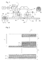
- Figure 1 schematically depicts a lithographic projection apparatus according to a particular embodiment of the invention.
- the apparatus comprises:
- the apparatus is of a reflective type (i.e. has a reflective mask). However, in general, it may also be of a transmissive type, for example (with a transmissive mask). Alternatively, the apparatus may employ another kind of patterning means, such as a programmable mirror array of a type as referred to above.
- the source LA (e.g. a laser-produced or discharge plasma source) produces a beam of radiation.
- This beam is fed into an illumination system (illuminator) IL, either directly or after having traversed conditioning means, such as a beam expander Ex, for example.
- the illuminator IL may comprise adjusting means AM for setting the outer and/or inner radial extent (commonly referred to as ⁇ -outer and ⁇ -inner, respectively) of the intensity distribution in the beam.
- ⁇ -outer and ⁇ -inner commonly referred to as ⁇ -outer and ⁇ -inner, respectively
- it will generally comprise various other components, such as an integrator IN and a condenser CO.
- the beam PB impinging on the mask MA has a desired intensity distribution in its cross-section.
- the source LA may be within the housing of the lithographic projection apparatus (as is often the case when the source LA is a mercury lamp, for example), but that it may also be remote from the lithographic projection apparatus, the radiation beam which it produces being led into the apparatus ( e.g . with the aid of suitable directing mirrors); this latter scenario is often the case when the source LA is an excimer laser.
- the current invention and Claims encompass both of these scenarios.
- the beam PB subsequently intercepts the mask MA, which is held on a mask table MT. Having been selectively reflected by the mask MA, the beam PB passes through the lens PL, which focuses the beam PB onto a target portion C of the substrate W. With the aid of the second positioning means (and interferometric measuring means IF), the substrate table WT can be moved accurately, e.g. so as to position different target portions C in the path of the beam PB. Similarly, the first positioning means can be used to accurately position the mask MA with respect to the path of the beam PB, e.g. after mechanical retrieval of the mask MA from a mask library, or during a scan.
- the mask table MT may just be connected to a short stroke actuator, or may be fixed.
- the depicted apparatus can be used in two different modes:
- Figure 2 shows a reflector 1 used in the first embodiment of the invention.
- the reflector 1 comprises a multilayer stack 2, e.g. comprising alternating layers of Molybdenum 21 and Silicon 22, grown on a substrate 4.
- additional multilayers 4 are added locally, as necessary to provide the desired correction.
- the additional multilayers 4 may be made of alternating layers 41, 42 of the same materials as the multilayer stack 2, e.g. Molybdenum and Silicon, but have their thicknesses, optimized for the desired phase change. Mathematical techniques for optimization of the various layer thicknesses as described in European Patent Applications EP-A-1 065 532 and EP-A-1 065 568 may be used.
- interferometric techniques can be used.
- Figure 3 shows the phase change ⁇ (open circles), in units of ⁇ radians, achievable for the addition of 1, 2, 3, 4, 5 or 10 periods of Mo/Si as well as resulting increases in reflectivity (open squares).
- the dashed line is a least squares fit to the phase change values.
- the notation x-y/z (with x optional) is used to describe a period of a multilayer stack where y, and optionally x, may be denoted as an absorbing material and z as a spacer material.
- the base period is enclosed in ⁇ and the additional layers in ().
- a multilayer is "tuned” if the total optical thickness (physical thickness multiplied by refractive index) of its period is equal to half the wavelength of the incident radiation, taking into account the angle of incidence as necessary.
- Ru can be used in place of or in addition to Mo and Y can be used in place of Si.
- Figure 4 shows the phase shift ⁇ , in units of ⁇ radians, achievable for the addition of 1 to 10 periods of Mo/Y (open triangles), Ru-Mo/Si (filled circles) arid Rh/Si (open squares) to a fifty period Mo/Si multilayer.
- the results of Figure 3 for the addition of optimized Mo/Si layers (open circles) are also shown for comparison.
- Figure 4 shows that the use of Ru-Mo in place of Mo and Y in place of Si can provide greater phase changes (sensitivities) for the same physical thickness of additional layers.
- the Ru and Mo layer thicknesses were fixed at 2nm but may of course be optimized as desired.
- phase changes of the additional multilayers are given with respect to a hypothetical "vacuum layer" of the same thickness as the added multilayers.
- the designs presented in Figures 3 and 4 include a final capping layer, whereas the designs of Table 1 denote, giving rise to a slight difference in presented values for comparable designs.
- Table 1 below gives calculated phase sensitivities for various multilayer structures useable as additional layers in the invention. It will be seen by comparing designs 1 and 2 that the phase sensitivity per period ⁇ increases form 0.043 ⁇ to 0.054 ⁇ as the Mo thickness is deliberately set to 4.0nm. Similarly, Ru/Si designs 3 and 4 exhibit a large change in ⁇ as the Ru thickness is increased form 1.98nm to 3.50nm. This is because of the lower n of Ru compared to Mo but the higher extinction coefficient of Ru means that there is a significant drop in peak reflectivity. The three-component Ru-Mo/Si additional layers maintain high peak reflectivities even as the Ru and Mo thicknesses are increased, with designs 6 and 7 exhibiting particularly high values of ⁇ . The yttriumbased stacks exhibit the greatest phase sensitivity due to the significant contribution of Y to the phase change with respect to vacuum.
- any figure error may be corrected by adding additional multilayers at those locations that exhibit a "valley"-like figure error.
- Another approach is to add the additional multilayers over the whole of the reflective surface and will away some or all of the added multilayers, as required, at those locations that exhibit a "hill"-like figure error.
- Filler stacks presenting a small or negligible phase change (as will be described in embodiment 2) may be added in between the additional multilayers presenting a large phase change to and-up-with an approximately level reflective surface.
- the second embodiment of the present invention provides a phase shift mask for use at EUV wavelengths.
- the phase shift mask can be used in a lithographic apparatus as described with reference to Figure 1, with or without the corrected reflectors described above.
- a phase shift reflective mask 50 is shown in Figure 5 of the accompanying drawings.
- This comprises a base multilayer stack 51 each period of which comprises a layer of absorbing material 51a and a layer of a spacer material 51b.
- a phase shifting stack 52 again each period of which comprises a layer of absorbing material 52a and a layer of a spacer material 52b, and a filler stack 53, each period of which also comprises a layer of absorbing material 53a and a layer of a spacer material 53b.
- the phase shifting stack 52 and filler stack 53 are arranged in a-pattern as necessary to pattern the projection beam to cause the desired image to be projected onto the substrate. Design rules for the phase shift mask of the present invention can be adapted as necessary from those employed for phase shift masks at other frequencies.
- phase shift mask of the present embodiment exploits the ability described above to provide multilayer stacks with both large phase sensitivities and small phase sensitivities.
- a phase shift mask necessitates selectively shifting the optical wavefront by, for instance, ⁇ radians.
- a ⁇ radian (or any other value such as ⁇ /2) phase change is readily achievable with respect to a "vacuum layer" or with respect to a filler multilayer (e.g. designs 9 and 10 in table 1), albeit at the expense of some reflectivity.
- a ⁇ phase shift is shown between the a phase shifting stack 52 of Ru-Mo/Si (design 7 in table 1) and a filler stack of Pd/Si (design 9 in table 1) after approximately 11 periods.
- An advantage of such a phase shift mask with a ⁇ -radian phase change with respect to a filler stack is that the surface of the mask may be level to within ⁇ 3 nm.
Landscapes
- Physics & Mathematics (AREA)
- Engineering & Computer Science (AREA)
- General Physics & Mathematics (AREA)
- Chemical & Material Sciences (AREA)
- Nanotechnology (AREA)
- Crystallography & Structural Chemistry (AREA)
- Manufacturing & Machinery (AREA)
- Epidemiology (AREA)
- Mathematical Physics (AREA)
- Condensed Matter Physics & Semiconductors (AREA)
- Optics & Photonics (AREA)
- Health & Medical Sciences (AREA)
- Environmental & Geological Engineering (AREA)
- Theoretical Computer Science (AREA)
- Public Health (AREA)
- Spectroscopy & Molecular Physics (AREA)
- General Engineering & Computer Science (AREA)
- High Energy & Nuclear Physics (AREA)
- Exposure And Positioning Against Photoresist Photosensitive Materials (AREA)
- Exposure Of Semiconductors, Excluding Electron Or Ion Beam Exposure (AREA)
- Optical Elements Other Than Lenses (AREA)
- Preparing Plates And Mask In Photomechanical Process (AREA)
Priority Applications (7)
| Application Number | Priority Date | Filing Date | Title |
|---|---|---|---|
| EP01304452A EP1260861A1 (de) | 2001-05-21 | 2001-05-21 | Methode zur Herstellung eines Reflektors, Reflektor und Phasenverschiebungsmaske sowie Lithographiegerät |
| EP02253475A EP1260862B1 (de) | 2001-05-21 | 2002-05-17 | Lithographisches Gerät, Methoden zur Herstellung von Bauelementen, Methode zur Herstellung eines Reflektors sowie eine Phasenschiebermaske |
| JP2002142416A JP3766041B2 (ja) | 2001-05-21 | 2002-05-17 | リソグラフィ装置、デバイス製造方法、この方法によって製造されるデバイス、反射器製造方法、この方法によって製造される反射器、位相シフト・マスク |
| KR1020020027368A KR100589235B1 (ko) | 2001-05-21 | 2002-05-17 | 리소그래피장치, 디바이스제조방법, 그 디바이스,반사기제조방법, 그 반사기 및 위상반전마스크 |
| TW091110390A TW567534B (en) | 2001-05-21 | 2002-05-17 | Lithographic projection apparatus, method of manufacturing integrated circuits, method of manufacturing a reflector, and phase shift mask |
| US10/147,309 US6777140B2 (en) | 2001-05-21 | 2002-05-17 | Lithographic apparatus, device manufacturing methods, devices manufactured thereby, method of manufacturing a reflector, reflector manufactured thereby and phase shift mask |
| US10/896,020 US6985211B2 (en) | 2001-05-21 | 2004-07-22 | Lithographic apparatus, device manufacturing methods, devices manufactured thereby, method of manufacturing a reflector, reflector manufactured thereby and phase shift mask |
Applications Claiming Priority (1)
| Application Number | Priority Date | Filing Date | Title |
|---|---|---|---|
| EP01304452A EP1260861A1 (de) | 2001-05-21 | 2001-05-21 | Methode zur Herstellung eines Reflektors, Reflektor und Phasenverschiebungsmaske sowie Lithographiegerät |
Publications (1)
| Publication Number | Publication Date |
|---|---|
| EP1260861A1 true EP1260861A1 (de) | 2002-11-27 |
Family
ID=8181970
Family Applications (1)
| Application Number | Title | Priority Date | Filing Date |
|---|---|---|---|
| EP01304452A Withdrawn EP1260861A1 (de) | 2001-05-21 | 2001-05-21 | Methode zur Herstellung eines Reflektors, Reflektor und Phasenverschiebungsmaske sowie Lithographiegerät |
Country Status (5)
| Country | Link |
|---|---|
| US (2) | US6777140B2 (de) |
| EP (1) | EP1260861A1 (de) |
| JP (1) | JP3766041B2 (de) |
| KR (1) | KR100589235B1 (de) |
| TW (1) | TW567534B (de) |
Cited By (6)
| Publication number | Priority date | Publication date | Assignee | Title |
|---|---|---|---|---|
| WO2004006017A1 (ja) * | 2002-07-02 | 2004-01-15 | Sony Corporation | 位相シフトマスクおよびその製造方法並びに半導体装置の製造方法 |
| US7952797B2 (en) | 2003-03-03 | 2011-05-31 | Carl Zeiss Smt Gmbh | Reflective optical element and EUV lithography appliance |
| US8003960B2 (en) | 2003-04-25 | 2011-08-23 | Carl Zeiss Smt Gmbh | Reflective optical element, optical system and EUV lithography device |
| CN104656376A (zh) * | 2013-11-15 | 2015-05-27 | 台湾积体电路制造股份有限公司 | 远紫外线光刻工艺和掩模 |
| WO2020081842A1 (en) * | 2018-10-17 | 2020-04-23 | Astrileux Corporation | Photomask having reflective layer with non-reflective regions |
| KR20210124252A (ko) * | 2019-02-07 | 2021-10-14 | 에이에스엠엘 네델란즈 비.브이. | 패터닝 디바이스 및 그 사용 방법 |
Families Citing this family (15)
| Publication number | Priority date | Publication date | Assignee | Title |
|---|---|---|---|---|
| EP2854159B1 (de) * | 2003-06-02 | 2018-06-20 | Nikon Corporation | Mehrschichtfilmreflektor und Röntgenstrahlexpositionssystem |
| US7499149B2 (en) * | 2003-06-24 | 2009-03-03 | Asml Netherlands B.V. | Holographic mask for lithographic apparatus and device manufacturing method |
| DE10330421A1 (de) | 2003-07-04 | 2005-02-03 | Leonhard Kurz Gmbh & Co. Kg | Belichtungsstation für Folienbahnen |
| JP2005302963A (ja) * | 2004-04-09 | 2005-10-27 | Canon Inc | 露光装置 |
| US6960775B1 (en) * | 2004-04-13 | 2005-11-01 | Asml Netherlands B.V. | Lithographic apparatus, device manufacturing method and device manufactured thereby |
| JP2005311145A (ja) * | 2004-04-23 | 2005-11-04 | Canon Inc | 露光装置、露光方法、デバイス製造方法、パターン形成装置および位置合わせ方法 |
| JP4569276B2 (ja) * | 2004-11-26 | 2010-10-27 | オムロン株式会社 | 干渉計 |
| FR2884965B1 (fr) | 2005-04-26 | 2007-06-08 | Commissariat Energie Atomique | Structure de blanc de masque ajustable pour masque euv a decalage de phase |
| JP2007134464A (ja) * | 2005-11-09 | 2007-05-31 | Canon Inc | 多層膜を有する光学素子及びそれを有する露光装置 |
| JP2007140105A (ja) * | 2005-11-18 | 2007-06-07 | Nikon Corp | 多層膜反射鏡及び露光装置 |
| KR100735531B1 (ko) | 2006-03-21 | 2007-07-04 | 삼성전자주식회사 | 보상 패턴을 포함하는 반사형 포토마스크와 그 제조방법 및반사형 블랭크 포토마스크 |
| US7771896B2 (en) * | 2006-12-22 | 2010-08-10 | Asml Netherlands B.V. | Patterning device, method of providing a patterning device, photolithographic apparatus and device manufacturing method |
| DE102011005144A1 (de) * | 2010-03-17 | 2011-09-22 | Carl Zeiss Smt Gmbh | Reflektives optisches Element, Projektionssystem und Projektionsbelichtungsanlage |
| JP6136445B2 (ja) * | 2013-03-27 | 2017-05-31 | 凸版印刷株式会社 | 反射型位相シフトマスク及び製造方法 |
| TWI650607B (zh) * | 2014-10-21 | 2019-02-11 | 日商Agc股份有限公司 | Euvl用附反射層之基板及其製造方法、以及euvl用反射型光罩基底及euvl用反射型光罩 |
Citations (2)
| Publication number | Priority date | Publication date | Assignee | Title |
|---|---|---|---|---|
| EP0708367A1 (de) * | 1994-10-20 | 1996-04-24 | AT&T Corp. | Gerät zur Darstellung von Mustern zum Einsatz im extremen UV-Bereich |
| US6159643A (en) * | 1999-03-01 | 2000-12-12 | Advanced Micro Devices, Inc. | Extreme ultraviolet lithography reflective mask |
Family Cites Families (15)
| Publication number | Priority date | Publication date | Assignee | Title |
|---|---|---|---|---|
| JP2545905B2 (ja) * | 1987-12-29 | 1996-10-23 | キヤノン株式会社 | 反射型マスクならびにこれを用いた露光方法 |
| JPH03266842A (ja) | 1990-03-16 | 1991-11-27 | Fujitsu Ltd | 反射型ホトリソグラフィ方法、反射型ホトリソグラフィ装置および反射型ホトマスク |
| JP3047541B2 (ja) * | 1991-08-22 | 2000-05-29 | 株式会社日立製作所 | 反射型マスクおよび欠陥修正方法 |
| JPH05134385A (ja) | 1991-11-11 | 1993-05-28 | Nikon Corp | 反射マスク |
| US5958629A (en) * | 1997-12-22 | 1999-09-28 | Intel Corporation | Using thin films as etch stop in EUV mask fabrication process |
| JPH11305417A (ja) | 1998-04-24 | 1999-11-05 | Hitachi Ltd | 露光方法および反射型マスク |
| JPH11352669A (ja) * | 1998-06-05 | 1999-12-24 | Hitachi Ltd | 露光方法および反射型マスク |
| JP2001057328A (ja) * | 1999-08-18 | 2001-02-27 | Nikon Corp | 反射マスク、露光装置および集積回路の製造方法 |
| US6562522B1 (en) * | 1999-10-29 | 2003-05-13 | Intel Corporation | Photomasking |
| AU2807401A (en) | 1999-11-29 | 2001-06-12 | Tohoku Techno Arch Co., Ltd. | Optical element such as multilayer film reflection mirror, production method therefor and device using it |
| US6410193B1 (en) * | 1999-12-30 | 2002-06-25 | Intel Corporation | Method and apparatus for a reflective mask that is inspected at a first wavelength and exposed during semiconductor manufacturing at a second wavelength |
| US6479195B1 (en) * | 2000-09-15 | 2002-11-12 | Intel Corporation | Mask absorber for extreme ultraviolet lithography |
| US6589717B1 (en) * | 2000-11-17 | 2003-07-08 | Advanced Micro Devices, Inc. | Photon assisted deposition of hard mask formation for use in manufacture of both devices and masks |
| KR20020052468A (ko) * | 2000-12-26 | 2002-07-04 | 박종섭 | 반도체 소자의 얼터내이팅 위상 반전 마스크 제조방법 |
| US6593037B1 (en) * | 2001-05-02 | 2003-07-15 | Advanced Micro Devices, Inc. | EUV mask or reticle having reduced reflections |
-
2001
- 2001-05-21 EP EP01304452A patent/EP1260861A1/de not_active Withdrawn
-
2002
- 2002-05-17 KR KR1020020027368A patent/KR100589235B1/ko not_active Expired - Fee Related
- 2002-05-17 US US10/147,309 patent/US6777140B2/en not_active Expired - Lifetime
- 2002-05-17 TW TW091110390A patent/TW567534B/zh not_active IP Right Cessation
- 2002-05-17 JP JP2002142416A patent/JP3766041B2/ja not_active Expired - Fee Related
-
2004
- 2004-07-22 US US10/896,020 patent/US6985211B2/en not_active Expired - Lifetime
Patent Citations (2)
| Publication number | Priority date | Publication date | Assignee | Title |
|---|---|---|---|---|
| EP0708367A1 (de) * | 1994-10-20 | 1996-04-24 | AT&T Corp. | Gerät zur Darstellung von Mustern zum Einsatz im extremen UV-Bereich |
| US6159643A (en) * | 1999-03-01 | 2000-12-12 | Advanced Micro Devices, Inc. | Extreme ultraviolet lithography reflective mask |
Non-Patent Citations (1)
| Title |
|---|
| CHOKSI N ET AL: "Maskless extreme ultraviolet lithography", 43RD INTERNATIONAL CONFERENCE ON ELECTRON, ION, AND PHOTON BEAM TECHNOLOGY AND NANOFABRICATION, MARCO ISLAND, FL, USA, 1-4 JUNE 1999, vol. 17, no. 6, Journal of Vacuum Science & Technology B (Microelectronics and Nanometer Structures), Nov. 1999, AIP for American Vacuum Soc, USA, pages 3047 - 3051, XP002183158, ISSN: 0734-211X * |
Cited By (12)
| Publication number | Priority date | Publication date | Assignee | Title |
|---|---|---|---|---|
| WO2004006017A1 (ja) * | 2002-07-02 | 2004-01-15 | Sony Corporation | 位相シフトマスクおよびその製造方法並びに半導体装置の製造方法 |
| US7952797B2 (en) | 2003-03-03 | 2011-05-31 | Carl Zeiss Smt Gmbh | Reflective optical element and EUV lithography appliance |
| US8243364B2 (en) | 2003-03-03 | 2012-08-14 | Carl Zeiss Smt Gmbh | Reflective optical element and EUV lithography appliance |
| US8537460B2 (en) | 2003-03-03 | 2013-09-17 | Carl Zeiss Smt Gmbh | Reflective optical element and EUV lithography appliance |
| US8891163B2 (en) | 2003-03-03 | 2014-11-18 | Carl Zeiss Smt Gmbh | Reflective optical element and EUV lithography appliance |
| US9910193B2 (en) | 2003-03-03 | 2018-03-06 | Carl Zeiss Smt Gmbh | Reflective optical element and EUV lithography appliance |
| US8003960B2 (en) | 2003-04-25 | 2011-08-23 | Carl Zeiss Smt Gmbh | Reflective optical element, optical system and EUV lithography device |
| US8633460B2 (en) | 2003-04-25 | 2014-01-21 | Carl Zeiss Smt Gmbh | Reflective optical element, optical system EUV and lithography device |
| CN104656376A (zh) * | 2013-11-15 | 2015-05-27 | 台湾积体电路制造股份有限公司 | 远紫外线光刻工艺和掩模 |
| CN104656376B (zh) * | 2013-11-15 | 2018-12-28 | 台湾积体电路制造股份有限公司 | 远紫外线光刻工艺和掩模 |
| WO2020081842A1 (en) * | 2018-10-17 | 2020-04-23 | Astrileux Corporation | Photomask having reflective layer with non-reflective regions |
| KR20210124252A (ko) * | 2019-02-07 | 2021-10-14 | 에이에스엠엘 네델란즈 비.브이. | 패터닝 디바이스 및 그 사용 방법 |
Also Published As
| Publication number | Publication date |
|---|---|
| JP3766041B2 (ja) | 2006-04-12 |
| JP2003059822A (ja) | 2003-02-28 |
| TW567534B (en) | 2003-12-21 |
| US20040263820A1 (en) | 2004-12-30 |
| US20030031938A1 (en) | 2003-02-13 |
| KR100589235B1 (ko) | 2006-06-14 |
| KR20030006968A (ko) | 2003-01-23 |
| US6777140B2 (en) | 2004-08-17 |
| US6985211B2 (en) | 2006-01-10 |
Similar Documents
| Publication | Publication Date | Title |
|---|---|---|
| US7466413B2 (en) | Marker structure, mask pattern, alignment method and lithographic method and apparatus | |
| US6985211B2 (en) | Lithographic apparatus, device manufacturing methods, devices manufactured thereby, method of manufacturing a reflector, reflector manufactured thereby and phase shift mask | |
| US6927004B2 (en) | Mask for use in lithography, method of making a mask, lithographic apparatus, and device manufacturing method | |
| US7759029B2 (en) | Substrate provided with an alignment mark in a substantially transmissive process layer, mask for exposing said mark, device manufacturing method, and device manufactured thereby | |
| KR101593534B1 (ko) | 정렬 타겟들을 위한 회절 요소들 | |
| EP1316851B1 (de) | Verfahren zur Mehrfachbelichtung mit Reduzierung der gedruckten Hilfsmuster | |
| US7391502B2 (en) | Lithographic apparatus, device manufacturing method, and method of manufacturing a component | |
| US6954257B2 (en) | Lithographic apparatus and device manufacturing method | |
| EP1260862B1 (de) | Lithographisches Gerät, Methoden zur Herstellung von Bauelementen, Methode zur Herstellung eines Reflektors sowie eine Phasenschiebermaske | |
| US20040120458A1 (en) | Method of fabricating an optical element, lithographic apparatus and device manufacturing method | |
| EP1400860B1 (de) | Lithographische Markierungsstruktur, lithographischer Projektionsapparat mit einer solchen Markierungsstruktur und Verfahren zur Ausrichtung eines Substrates unter Verwendung einer solchen Markierungsstruktur | |
| EP1260870A1 (de) | Ausrichtmarke | |
| EP1394815B1 (de) | Lithographiegerät mit einem Mo/Si Mehrfachschichtenspiegel mit einer Schutzschicht | |
| EP1260869A1 (de) | Substrat mit Ausrichtungsmarke in einer wesentlich transparenten Prozessschicht | |
| EP1426821B1 (de) | Methode zur Erzeugung eines optischen Elements, lithographischer Apparat sowie Methode zur Herstellung eines Geräts | |
| EP1357427B1 (de) | Lithographische Maske, lithographischer Apparat und Verfahren zur Herstellung einer Vorrichtung | |
| EP1416329A1 (de) | Lithographischer Projektionsapparat und Verfahren zur Herstellung einer Vorrichtung | |
| EP1498779A2 (de) | Ausrichtungs- oder Überlagerungs-Markenstruktur | |
| EP1369744A1 (de) | Lithographischer Apparat und Verfahren zur Herstellung einer Vorrichtung | |
| EP1500987A1 (de) | Lithographischer Apparat, Verfahren zur Herstellung eines Artikels und damit hergestellter Artikel |
Legal Events
| Date | Code | Title | Description |
|---|---|---|---|
| PUAI | Public reference made under article 153(3) epc to a published international application that has entered the european phase |
Free format text: ORIGINAL CODE: 0009012 |
|
| AK | Designated contracting states |
Kind code of ref document: A1 Designated state(s): AT BE CH CY DE DK ES FI FR GB GR IE IT LI LU MC NL PT SE TR |
|
| AX | Request for extension of the european patent |
Free format text: AL;LT;LV;MK;RO;SI |
|
| STAA | Information on the status of an ep patent application or granted ep patent |
Free format text: STATUS: THE APPLICATION IS DEEMED TO BE WITHDRAWN |
|
| 18D | Application deemed to be withdrawn |
Effective date: 20020903 |