EP1302776B1 - Automatische Abtastprüfung von komplexen integrierten Schaltungen - Google Patents
Automatische Abtastprüfung von komplexen integrierten Schaltungen Download PDFInfo
- Publication number
- EP1302776B1 EP1302776B1 EP01402617A EP01402617A EP1302776B1 EP 1302776 B1 EP1302776 B1 EP 1302776B1 EP 01402617 A EP01402617 A EP 01402617A EP 01402617 A EP01402617 A EP 01402617A EP 1302776 B1 EP1302776 B1 EP 1302776B1
- Authority
- EP
- European Patent Office
- Prior art keywords
- scan
- circuit elements
- signals
- during
- data
- Prior art date
- Legal status (The legal status is an assumption and is not a legal conclusion. Google has not performed a legal analysis and makes no representation as to the accuracy of the status listed.)
- Expired - Lifetime
Links
- 238000012360 testing method Methods 0.000 title abstract description 52
- 238000000034 method Methods 0.000 claims abstract description 24
- 230000004044 response Effects 0.000 claims abstract description 13
- 230000008569 process Effects 0.000 claims abstract description 10
- 238000010998 test method Methods 0.000 claims description 3
- 239000004020 conductor Substances 0.000 description 36
- 230000006870 function Effects 0.000 description 7
- 238000010586 diagram Methods 0.000 description 6
- 238000004519 manufacturing process Methods 0.000 description 3
- 239000000758 substrate Substances 0.000 description 3
- 239000013598 vector Substances 0.000 description 3
- 230000008901 benefit Effects 0.000 description 2
- 230000001934 delay Effects 0.000 description 2
- 230000000694 effects Effects 0.000 description 2
- 238000002546 full scan Methods 0.000 description 2
- 230000006872 improvement Effects 0.000 description 2
- 230000009467 reduction Effects 0.000 description 2
- 230000008859 change Effects 0.000 description 1
- 238000013481 data capture Methods 0.000 description 1
- 230000003247 decreasing effect Effects 0.000 description 1
- 230000007257 malfunction Effects 0.000 description 1
- 230000002093 peripheral effect Effects 0.000 description 1
- 230000000644 propagated effect Effects 0.000 description 1
Images


Classifications
-
- G—PHYSICS
- G01—MEASURING; TESTING
- G01R—MEASURING ELECTRIC VARIABLES; MEASURING MAGNETIC VARIABLES
- G01R31/00—Arrangements for testing electric properties; Arrangements for locating electric faults; Arrangements for electrical testing characterised by what is being tested not provided for elsewhere
- G01R31/28—Testing of electronic circuits, e.g. by signal tracer
- G01R31/317—Testing of digital circuits
- G01R31/3181—Functional testing
- G01R31/3185—Reconfiguring for testing, e.g. LSSD, partitioning
- G01R31/318533—Reconfiguring for testing, e.g. LSSD, partitioning using scanning techniques, e.g. LSSD, Boundary Scan, JTAG
- G01R31/318536—Scan chain arrangements, e.g. connections, test bus, analog signals
Definitions
- This invention relates generally to testing integrated circuits and more particularly to automatic scan-based testing of the functionality of complex integrated circuits.
- Complex integrated circuits often contain one or more embedded core data processors that communicate with peripherals, memory, or other circuitry on the same substrate.
- a method of automatic scan-based testing of such integrated circuits is described in US Patent N° 5 717 700, assigned to the present Applicant.
- the 'scan'-based test technique described in US Patent N° 5717 700 is a cost-effective solution to test the operation of integrated circuits, which include functional logic elements and register elements, such as flip-flop circuits or latches, with functional interconnections between the different elements.
- the integrated circuit design includes specific provision for re-configuring the interconnections of the elements of the integrated circuit so that test data signals entered serially at one or more input pins can be shifted ('scanned') along a scan chain different from the normal functional system path from one register element to another in order to place the signals of the test vector at the desired positions.
- the integrated circuit returns then temporarily to its normal functional system configuration for one or more clock pulses to produce test outputs corresponding to a particular logic function outcome from the normal logic functions in the integrated circuit, given the values of the test vector.
- the integrated circuit then reverts to the scan configuration and shifts out the test outputs along the scan chain to one or more output pins where they can be retrieved and compared with the expected results to diagnose faults.
- This scan-based test method has to be provided for during design of the integrated circuit ('Design-for-Test'). Additional scan interconnection routes for the scan chain are included linking alternative scan inputs and outputs for scan data parallel to the functional data inputs and outputs, and which are added to certain of the basic elements (flip-flops and latches) within the integrated circuits.
- the alternative input for scan data of a scan element may be implemented by placing a multiplexor in front of the standard input of the scan element to select either scan data or functional data.
- These 'scan configurable' elements are then connected together in a serial shift register fashion during the scan configuration by connecting the scan output of one element to the scan input of the next element of the scan chain in response to a scan_enable signal asserted on an 'enable' input of the scan configurable elements.
- the scan chain can then load scan test data (and simultaneously unload the test results that give internal integrated circuit state information) by allowing scan data to be transferred from one element to another on each active scan clock edge.
- the scan_enable signal After loading the scan test data to place the elements of the scan chain in a desired state for the test, the scan_enable signal is de-asserted (set to 'zero' if its asserted value is 'one') temporarily to use the functional data input of the scan elements to capture data from the logic circuit elements in functional mode for one or more clock cycles. The scan_enable signal is then re-asserted and the test results unloaded (and fresh scan test data for the next phase of the test simultaneously loaded).
- the technique of providing scan data in scan mode and switching to functional mode for more than one clock cycles may be employed to verify time delays of portions of the logic circuitry in the integrated circuit.
- the scan design has the effect of turning each selected sequential scan configurable device (flip-flop or latch) into an internal test point.
- the standard input is referred to as the D-input while the standard output is referred to as the Q-output
- the scan test data input and output being referred to as SD-input and SD-output respectively.
- the D-input of each scan configurable device is a settable test point and the Q-output a primary output test point while the SD-input and SD-output are data loading and unloading points in the scan chain.
- Partial-scan enables the test patterns developed for those modules also to be re-used in the new chip design. Partial-scan also offers an improvement in the availability of pins for introducing external scan test signals and more flexibility in the choice of different test techniques for different modules, for example.
- a potential problem for partial-scan is that the data input signals at certain points, especially at the interfaces (or 'gaskets') of the modules, for example, may not be controlled, that is to say the signal propagated may be 'unknown' (unpredictable). Even if the data input signals are controlled in the chip for which the module is first designed, it is desirable to provide for re-use of the module with a minimum of re-design of its architecture and software in future different chips. Accordingly, it is desirable to provide for selective control of at least certain scan test data input signals.
- Testing of substantially the whole chip may be obtained by dividing the complete chip into different scan domains, each incorporating several parallel scan chains, and whose boundaries may coincide in certain cases with the boundaries of the different modules; however, one module might include more than one domain or, more typically, one domain may include more than one module.
- the domains are separated during the scan configuration in response to a scan_mode signal.
- the scan data of the different domains are then entered and the tests of the different domains applied sequentially.
- Such a system and method is referred to herein as a 'domain scanning' test system and method.
- a boundary scan system for circuit boards is described in US Patents N° 5 450 415 and N° 6 115 827 it is possible to adapt such a boundary scan system for integrated circuits by adding flip-flop and multiplex elements, referred to as scan wrappers, to input end elements of the scan chains in the integrated circuits to define the values of the scan test data signals at each point where the signal would otherwise be unknown.
- scan wrappers flip-flop and multiplex elements
- this configuration creates substantial additional hardware (a large chip may include 7 scan domains and 30 or more modules each of which requires control of many unknown inputs at the interfaces), introduces an additional time lag in the system operational functions, is inflexible in terms of re-use of the modules in other future chips and the testing of the real functional path is sub-optimal.
- the present invention provides a method of testing an integrated circuit as described in the accompanying claims and an integrated circuit tested by a method as described in the accompanying claims
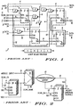
- Figure 1 illustrates a simplified module 1 in an integrated circuit.
- the module comprises logic elements 2 including gates and inverters, for example, and register elements 3, the logic elements 2 and register elements 3 being normally interconnected in a functional configuration by electrically conductive connections 4 between data input points 5 and data output points 6.
- the module 1 also includes a clock signal input point 7 to which clock signals are applied and asserted on corresponding clock inputs of the register elements 3 to enable a change of state of the register elements.
- the module 1 also includes a scan data input point 8 to which scan data signals are applied, the scan data input point 8 being the start of a scan chain comprising electrically conductive scan conductors 9 interconnecting the register elements 3 with the scan data input point 8, the scan data input SDI of the register elements 3 being connected to scan data outputs SDO of the previous register element 3 in the chain except for the first register element 3 in the chain, which is connected to the scan data input point 8 and the last register element 3 in the chain whose scan data output SDO is connected to a scan data output point 10.
- the module 1 also includes a scan enable input point 11, which is connected to scan enable conductors 12, connected to control inputs SEN of the register elements 3, the control input SEN switching the register elements from their normal data inputs D to the scan data inputs SDI when a scan_enable signal is asserted on the input 11.
- the logic elements 2 and the register elements 3 are connected by the conductors 4 between the data input point 5 and the data output point 6.
- the scan_enable signal applied to the scan enable input point 11 is not asserted so that the data inputs D of the register elements 3 are functional and not the scan data inputs SDI.
- the module then performs its normal functional operation in response to clock signals applied to the clock input point 7.
- the scan_enable signal applied to the scan enable input point 11 is asserted so that the scan data inputs SDI of the register elements 3 are operational instead of the functional data inputs D.
- Serial data applied to the scan data input 8 may then be shifted along the chain of register elements 3 in response to clock pulses applied to the clock input point 7 to load known data into the register elements 3 and set them to desired state.
- the scan_enable signal applied to the input point 11 is then de-asserted for one or more cycles of clock pulses so that the logic elements 2 and the register element 3 are interconnected again by the functional configuration of conductors 4 and the module 1 performs its logic function on data applied to the data input points 5 and the data loaded into the register elements 3.
- the scan_enable signal applied to the input point 11 is asserted again and the new state of the register elements 3 consecutive to the functioning of the module 1 with the loaded data is shifted out along the conductors 9 and the chain of register elements 3 to the scan data output point 10 where it may be compared with expected values of the test results to check the proper functioning of the module 1.
- the module 1 is shown with all of the register elements 3 connectible in the scan chain by scan conductors 9. However, it will be appreciated that in practice, especially with large modules, the architecture employed may be partial-scan in which only certain, selected ones of the register elements 3 are connected in the scan chain.
- FIG. 2 shows a previously proposed boundary scan system schematically.
- a register 3 is shown connected with the connector 4 supplying data, the conductor 12 supplying the scan_enable signal and a conductor 9 supplying the scan data input signal, the remainder of the logic elements being shown globally at 13.
- An additional register 14, such as a flip-flop circuit, is provided for a point whose inputs are treated as unknown and therefore to be controlled.
- the register 14 receives data inputs over the functional configuration conductors 4 within the module, scan data input signals over the scan chain conductors 9 and scan_enable signals over the conductors 12.
- the output of the register 14 is connected to the input of a multiplexor 15 that also receives a data input signal from the module data input point 5.
- a scan mode signal is applied to a control input 16 of the multiplexor 15 to select either the data input signal from the module data input point 5 in functional configuration or the output of the register 14 in scan and scan test configuration.
- the scan mode signal is asserted at 16 and initially the scan enable signal is asserted at 12 during a first shift phase 17, during which clock pulses are applied on the conductors 7.
- the desired scan data inputs are applied serially on the scan data input point 8 and transmitted over the scan configuration conductors 9 through the register elements 3.
- the scan enable signal is de-asserted on the conductors 12, which has the effect of forcing the D inputs of the register elements 3 and 14.
- the corresponding values then appear at the outputs of the register elements 3 and 14 as shown at 19.
- One or more clock pulses are applied at the clock input point 7, as shown at 20, so that the logic elements 13, which are now in the functional configuration, process the data over the connectors 4 interconnection.
- the scan_enable signal is then reasserted on the scan enable input point 11 to reconnect the register elements 3 and 14 in the scan configuration by conductors 9 and, during a second shift phase 22, clock pulses are applied again to the clock input point 7 to shift the data from the outputs of the register elements 3 and 14 serially to the output point 10.
- Figure 4 shows an embodiment of the present invention that avoids any need for an additional register such as 14 or an additional multiplexor such as 15.
- the scan mode signal on conductor 16 is applied directly to the scan enable input SEN of each of the normal register elements forming part of the module operational circuitry instead of the scan_enable signal, for those elements where it is desired to control the data that the register transmits over the functional configuration conductors 4 during the data capture phases 18 to 21 of the scan test.
- the scan mode signal on conductor 16 is asserted so that the corresponding register elements 3 capture the scan data input signals on the conductors 9 and not the data signals from the logic elements supplied over the conductors 4.
- Figure 5 shows the structure of those register elements 3 that are to have their inputs controlled in this manner.
- the register element 3 in this case is equivalent to a multiplexor sub-element 23 receiving as inputs the signals on the data conductor 4 from the logic element and the scan data signals on the conductor 9, the selection between the two inputs being made by the scan mode signal applied over conductor 16 to a control input of the multiplexor sub-element 23.
- the output of the multiplexor sub-element 23 is a "scan_always" signal that corresponds to the scan data signal during the whole of the scan test, including both the shift phases 17 and 22 and the test phases 18 to 21.
- the scan_always signal is applied to the data input of a simple digital flip flop 24 whose output gives the data signals on the conductor 4 and the scan data signals on the scan configuration conductors 9.
- groups of the register elements 3 whose data inputs over the lines 4 it may or may not be desired to control during the scan test process are connected to an additional multiplexor element 25, as many multiplexor elements 25 being provided as there are separate groups of register elements 3 that it may be desired to control separately.
- Each multiplexor element 25 has an input connected to a scan enable conductor 12 and another input connected to a scan mode conductor 16.
- a control input of the multiplexor 25 is connected to a respective conductor 26 to which a "scan_always_enable" signal is applied from an input point.
- the output of the multiplexor elements 25 are applied over "scan_always" conductors 27 to the scan enable inputs SEN of their respective groups of register elements 3.
- the scan_always_enable signal is asserted on line 26 for that group and the corresponding multiplexor 25 selects the scan mode signal on conductor 16 instead of the scan_enable signal on conductor 12.
- the scan mode signal is then applied on the scan_always conductor 27 to that group of register elements 3 in place of a scan_enable signal, and the scan mode signal, asserted if this domain is to be scanned, is asserted on the scan enable inputs SEN of that group of register elements 3 during the whole of the scan operation.
- the scan_always_enable signal on conductor 26 is de-asserted during the scan operation so that the corresponding multiplexor 25 selects the scan_enable signal on the conductor 12. This signal then appears at the scan_always conductor 27 and is applied to the scan enable input SEN of the corresponding group of register element 3, as shown in Figure 3.
Landscapes
- Engineering & Computer Science (AREA)
- General Engineering & Computer Science (AREA)
- Physics & Mathematics (AREA)
- General Physics & Mathematics (AREA)
- Tests Of Electronic Circuits (AREA)
- Test And Diagnosis Of Digital Computers (AREA)
- Semiconductor Integrated Circuits (AREA)
Claims (5)
- Verfahren zum Prüfen einer integrierten Schaltung, die Folgendes umfasst: Logikschaltungselemente (2, 13) und Abtastschaltungselemente (3), funktionale Verbindungen (4) zum Verbinden der Schaltungselemente (2, 3, 13) in einer funktionalen Konfiguration zum Verarbeiten von Dateneingangssignalen, mindestens einen Abtastdatensignaleingang (8) und Abtastverbindungen (9) zum selektiven Verbinden der Abtastschaltungselemente (3) mit dem Abtastdateneingang (8) in einer Mehrzahl von Abtastdomänen in den jeweiligen Abtastkonfigurationen, wobei das Verfahren Folgendes umfasst: selektives Zuführen eines Abtastmodussignals zu den Abtastschaltungselementen (3), um eine der Abtastdomänen auszuwählen, Verbinden der Abtastschaltungselemente (3) der ausgewählten Abtastdomäne in der Abtastkonfiguration in Reaktion auf ein Abtastfreigabesignal, das an Abtastfreigabeeingängen (SEN) der Abtastschaltungselemente (3) mindestens der ausgewählten Abtastdomäne während einer ersten Abtastphase (17) anliegt, Zuführen von Abtastdatensignalen zu dem Abtastdateneingang (8), so dass die Abtastdatensignale sequentiell durch die verbundenen Abtastschaltungselemente (3) der entsprechenden Domäne in Reaktion auf Taktimpulse, die mindestens den Abtastschaltungselementen (3) während der ersten Abtastphase (17) zugeführt werden, verschoben und durch sie registriert werden, Verbinden mindestens der Schaltungselemente (2, 3, 13) der ausgewählten Abtastdomäne in der funktionalen Konfiguration während einer Erfassungsphase (18 bis 21) in Reaktion auf ein Nichtanliegen des Abtastfreigabesignals, so dass die funktionale Konfiguration der ausgewählten Abtastdomäne die Dateneingangssignale und die durch die Abtastschaltungselemente (3) registrierten Signale in Reaktion auf Taktimpulse, die den Schaltungselementen während der Erfassungsphase (18 bis 21) zugeführt werden, verarbeitet, erneutes Verbinden der Abtastschaltungselemente (3) der ausgewählten Abtastdomäne in der Abtastkonfiguration in Reaktion auf ein Neuanliegen des Abtastfreigabesignals während einer zweiten Abtastphase (22), um so die Ausgangssignale der Abtastschaltungselemente (3) der ausgewählten Abtastdomäne zu mindestens einem Abtastdatensignalausgang (10) in Reaktion darauf, dass die Taktimpulse den Abtastschaltungselementen (3) während der zweiten Abtastphase (22) zugeführt werden, zu verschieben, und Vergleichen der tatsächlichen Ausgangssignale aus dem Abtastdatensignalausgang (10) mit den erwarteten Abtastausgangssignalen, dadurch gekennzeichnet, dass die Abtastschaltungselemente (3) von einer Gruppe in der ausgewählten Abtastdomäne mit anderen Schaltungselementen entsprechend der Abtastkonfiguration in Reaktion auf das Abtastmodussignal mindestens während der Erfassungsphase (18 bis 21) verbunden werden, um dadurch die von der Abtastkonfiguration während der Erfassungsphase (18 bis 21) empfangenen Signale zu verarbeiten.
- Verfahren gemäß Anspruch 1, dadurch gekennzeichnet, dass das Abtastmodussignal an den Abtastfreigabeeingängen (SEN) der Abtastschaltungselemente (3) der Gruppe mindestens während der Erfassungsphase anliegt.
- Verfahren gemäß einem beliebigen der vorhergehenden Ansprüche, bei dem für eine Mehrzahl der Abtastschaltungselemente (3) die Abtastauswahlsignale (Abtast-immer-frei) anliegen oder nicht, um zwischen dem Abtastfreigabesignal und dem Abtastmodussignal auszuwählen, um selektive Abtastsignale (Abtast-immer) zu erzeugen, die den Abtastfreigabeeingängen (SEN) der Mehrzahl von Abtastschaltungselementen (3) mindestens während der Erfassungsphase (18 bis 21) zugeführt werden, um so auszuwählen, ob die Abtastschaltungselemente (3) der Mehrzahl von Abtastschaltungselementen in die Gruppe und die von der Abtastkonfiguration empfangenen Prozesssignale eingefügt werden oder ob sie von der Gruppe und den von der funktionalen Konfiguration während der Erfassungsphase (18 bis 21) empfangenen Prozesssignalen ausgeschlossen werden.
- Integrierte Schaltung, die alle in Anspruch 1 dargelegten Komponenten umfasst und durch ein Verfahren gemäß Anspruch 2 geprüft wird, bei der mindestens eine Mehrzahl von Abtastfreigabeeingängen (SEN) der Abtastschaltungselemente (3) der Gruppe verbunden ist, um das Abtastmodussignal zu empfangen.
- Integrierte Schaltung, die alle in Anspruch 1 dargelegten Komponenten umfasst und durch ein Verfahren gemäß Anspruch 3 geprüft wird, die eine Mehrzahl von Auswahlschaltungselementen (25) mit Abtastauswahleingängen umfasst, an denen Abtastauswahlsignale (Abtast-Immer-Frei) anliegen können, um zwischen dem Abtastfreigabesignal und dem Abtastmodussignal auszuwählen, um die selektiven Abtastsignale (Abtast-Immer) zu erzeugen, wobei die Auswahlschaltungselemente (25) verbunden sind, um das ausgewählte Signal mehr als einem der Abtastschaltungselemente zuzuführen.
Priority Applications (7)
| Application Number | Priority Date | Filing Date | Title |
|---|---|---|---|
| DE60105168T DE60105168T2 (de) | 2001-10-10 | 2001-10-10 | Automatische Abtastprüfung von komplexen integrierten Schaltungen |
| AT01402617T ATE274705T1 (de) | 2001-10-10 | 2001-10-10 | Automatische abtastprüfung von komplexen integrierten schaltungen |
| EP01402617A EP1302776B1 (de) | 2001-10-10 | 2001-10-10 | Automatische Abtastprüfung von komplexen integrierten Schaltungen |
| US10/491,658 US20050039093A1 (en) | 2001-10-10 | 2002-10-01 | Automatic scan-based testing of complex integrated circuits |
| JP2003536764A JP2005505781A (ja) | 2001-10-10 | 2002-10-01 | 複雑な集積回路の自動的なスキャン・ベースのテスト |
| KR10-2004-7005275A KR20040050908A (ko) | 2001-10-10 | 2002-10-01 | 복합 집적 회로들의 자동 스캔 방식 테스팅 |
| PCT/EP2002/010998 WO2003034083A2 (en) | 2001-10-10 | 2002-10-01 | Automatic scan-based testing of complex integrated circuits |
Applications Claiming Priority (1)
| Application Number | Priority Date | Filing Date | Title |
|---|---|---|---|
| EP01402617A EP1302776B1 (de) | 2001-10-10 | 2001-10-10 | Automatische Abtastprüfung von komplexen integrierten Schaltungen |
Publications (2)
| Publication Number | Publication Date |
|---|---|
| EP1302776A1 EP1302776A1 (de) | 2003-04-16 |
| EP1302776B1 true EP1302776B1 (de) | 2004-08-25 |
Family
ID=8182919
Family Applications (1)
| Application Number | Title | Priority Date | Filing Date |
|---|---|---|---|
| EP01402617A Expired - Lifetime EP1302776B1 (de) | 2001-10-10 | 2001-10-10 | Automatische Abtastprüfung von komplexen integrierten Schaltungen |
Country Status (7)
| Country | Link |
|---|---|
| US (1) | US20050039093A1 (de) |
| EP (1) | EP1302776B1 (de) |
| JP (1) | JP2005505781A (de) |
| KR (1) | KR20040050908A (de) |
| AT (1) | ATE274705T1 (de) |
| DE (1) | DE60105168T2 (de) |
| WO (1) | WO2003034083A2 (de) |
Families Citing this family (5)
| Publication number | Priority date | Publication date | Assignee | Title |
|---|---|---|---|---|
| CN100395557C (zh) * | 2005-03-04 | 2008-06-18 | 清华大学 | 采用加权扫描选通信号的基于扫描的自测试结构的自测试方法 |
| US20130275824A1 (en) * | 2012-04-12 | 2013-10-17 | Lsi Corporation | Scan-based capture and shift of interface functional signal values in conjunction with built-in self-test |
| GB2520506B (en) * | 2013-11-21 | 2020-07-29 | Advanced Risc Mach Ltd | Partial Scan Cell |
| CN106226678B (zh) * | 2016-07-15 | 2019-02-15 | 中国人民解放军国防科学技术大学 | 一种基于并行施加测试激励的低功耗扫描测试方法及装置 |
| US12449472B2 (en) * | 2022-09-27 | 2025-10-21 | Infineon Technologies Ag | Circuit and method for testing a circuit |
Family Cites Families (3)
| Publication number | Priority date | Publication date | Assignee | Title |
|---|---|---|---|---|
| US4710931A (en) * | 1985-10-23 | 1987-12-01 | Texas Instruments Incorporated | Partitioned scan-testing system |
| US5696771A (en) * | 1996-05-17 | 1997-12-09 | Synopsys, Inc. | Method and apparatus for performing partial unscan and near full scan within design for test applications |
| CA2225879C (en) * | 1997-12-29 | 2001-05-01 | Jean-Francois Cote | Clock skew management method and apparatus |
-
2001
- 2001-10-10 DE DE60105168T patent/DE60105168T2/de not_active Expired - Fee Related
- 2001-10-10 EP EP01402617A patent/EP1302776B1/de not_active Expired - Lifetime
- 2001-10-10 AT AT01402617T patent/ATE274705T1/de not_active IP Right Cessation
-
2002
- 2002-10-01 WO PCT/EP2002/010998 patent/WO2003034083A2/en not_active Ceased
- 2002-10-01 JP JP2003536764A patent/JP2005505781A/ja active Pending
- 2002-10-01 US US10/491,658 patent/US20050039093A1/en not_active Abandoned
- 2002-10-01 KR KR10-2004-7005275A patent/KR20040050908A/ko not_active Withdrawn
Also Published As
| Publication number | Publication date |
|---|---|
| WO2003034083A3 (en) | 2003-12-24 |
| DE60105168T2 (de) | 2005-01-27 |
| WO2003034083A2 (en) | 2003-04-24 |
| ATE274705T1 (de) | 2004-09-15 |
| DE60105168D1 (de) | 2004-09-30 |
| JP2005505781A (ja) | 2005-02-24 |
| KR20040050908A (ko) | 2004-06-17 |
| US20050039093A1 (en) | 2005-02-17 |
| EP1302776A1 (de) | 2003-04-16 |
Similar Documents
| Publication | Publication Date | Title |
|---|---|---|
| US5173904A (en) | Logic circuits systems, and methods having individually testable logic modules | |
| US4860290A (en) | Logic circuit having individually testable logic modules | |
| US5717700A (en) | Method for creating a high speed scan-interconnected set of flip-flop elements in an integrated circuit to enable faster scan-based testing | |
| US5260949A (en) | Scan path system and an integrated circuit device using the same | |
| US5719878A (en) | Scannable storage cell and method of operation | |
| US6711707B2 (en) | Process of controlling plural test access ports | |
| US4914379A (en) | Semiconductor integrated circuit and method of testing same | |
| US7409612B2 (en) | Testing of integrated circuits | |
| US5477545A (en) | Method and apparatus for testing of core-cell based integrated circuits | |
| US5084874A (en) | Enhanced test circuit | |
| US5717695A (en) | Output pin for selectively outputting one of a plurality of signals internal to a semiconductor chip according to a programmable register for diagnostics | |
| US7925942B2 (en) | Augmentation instruction shift register with serial and two parallel inputs | |
| US7124340B2 (en) | Low pin count, high-speed boundary scan testing | |
| US5488614A (en) | Integrated logic circuit | |
| JP2000275303A (ja) | バウンダリスキャンテスト方法及びバウンダリスキャンテスト装置 | |
| US5513186A (en) | Method and apparatus for interconnect testing without speed degradation | |
| US4742293A (en) | Pseudo-memory circuit for testing for stuck open faults | |
| US5703884A (en) | Scanning pass test circuit | |
| US4856002A (en) | Semiconductor integrated circuit apparatus | |
| US5894548A (en) | Semiconductor device having test circuit | |
| EP1302776B1 (de) | Automatische Abtastprüfung von komplexen integrierten Schaltungen | |
| US4829237A (en) | Circuit device having a self-testing function and a testing method thereof | |
| US6519728B2 (en) | Semiconductor integrated circuit having test circuit | |
| US6061284A (en) | Core test control | |
| US5130989A (en) | Serial and parallel scan technique for improved testing of systolic arrays |
Legal Events
| Date | Code | Title | Description |
|---|---|---|---|
| PUAI | Public reference made under article 153(3) epc to a published international application that has entered the european phase |
Free format text: ORIGINAL CODE: 0009012 |
|
| AK | Designated contracting states |
Designated state(s): AT BE CH CY DE DK ES FI FR GB GR IE IT LI LU MC NL PT SE TR |
|
| AX | Request for extension of the european patent |
Extension state: AL LT LV MK RO SI |
|
| 17P | Request for examination filed |
Effective date: 20031016 |
|
| AKX | Designation fees paid |
Designated state(s): AT BE CH CY DE DK ES FI FR GB GR IE IT LI LU MC NL PT SE TR |
|
| GRAP | Despatch of communication of intention to grant a patent |
Free format text: ORIGINAL CODE: EPIDOSNIGR1 |
|
| GRAS | Grant fee paid |
Free format text: ORIGINAL CODE: EPIDOSNIGR3 |
|
| GRAA | (expected) grant |
Free format text: ORIGINAL CODE: 0009210 |
|
| AK | Designated contracting states |
Kind code of ref document: B1 Designated state(s): AT BE CH CY DE DK ES FI FR GB GR IE IT LI LU MC NL PT SE TR |
|
| PG25 | Lapsed in a contracting state [announced via postgrant information from national office to epo] |
Ref country code: CY Free format text: LAPSE BECAUSE OF FAILURE TO SUBMIT A TRANSLATION OF THE DESCRIPTION OR TO PAY THE FEE WITHIN THE PRESCRIBED TIME-LIMIT Effective date: 20040825 Ref country code: LI Free format text: LAPSE BECAUSE OF FAILURE TO SUBMIT A TRANSLATION OF THE DESCRIPTION OR TO PAY THE FEE WITHIN THE PRESCRIBED TIME-LIMIT Effective date: 20040825 Ref country code: FI Free format text: LAPSE BECAUSE OF FAILURE TO SUBMIT A TRANSLATION OF THE DESCRIPTION OR TO PAY THE FEE WITHIN THE PRESCRIBED TIME-LIMIT Effective date: 20040825 Ref country code: CH Free format text: LAPSE BECAUSE OF FAILURE TO SUBMIT A TRANSLATION OF THE DESCRIPTION OR TO PAY THE FEE WITHIN THE PRESCRIBED TIME-LIMIT Effective date: 20040825 Ref country code: BE Free format text: LAPSE BECAUSE OF FAILURE TO SUBMIT A TRANSLATION OF THE DESCRIPTION OR TO PAY THE FEE WITHIN THE PRESCRIBED TIME-LIMIT Effective date: 20040825 Ref country code: AT Free format text: LAPSE BECAUSE OF FAILURE TO SUBMIT A TRANSLATION OF THE DESCRIPTION OR TO PAY THE FEE WITHIN THE PRESCRIBED TIME-LIMIT Effective date: 20040825 Ref country code: NL Free format text: LAPSE BECAUSE OF FAILURE TO SUBMIT A TRANSLATION OF THE DESCRIPTION OR TO PAY THE FEE WITHIN THE PRESCRIBED TIME-LIMIT Effective date: 20040825 Ref country code: TR Free format text: LAPSE BECAUSE OF FAILURE TO SUBMIT A TRANSLATION OF THE DESCRIPTION OR TO PAY THE FEE WITHIN THE PRESCRIBED TIME-LIMIT Effective date: 20040825 |
|
| REG | Reference to a national code |
Ref country code: GB Ref legal event code: FG4D |
|
| REG | Reference to a national code |
Ref country code: CH Ref legal event code: EP |
|
| REG | Reference to a national code |
Ref country code: IE Ref legal event code: FG4D |
|
| REF | Corresponds to: |
Ref document number: 60105168 Country of ref document: DE Date of ref document: 20040930 Kind code of ref document: P |
|
| PG25 | Lapsed in a contracting state [announced via postgrant information from national office to epo] |
Ref country code: LU Free format text: LAPSE BECAUSE OF NON-PAYMENT OF DUE FEES Effective date: 20041010 |
|
| PG25 | Lapsed in a contracting state [announced via postgrant information from national office to epo] |
Ref country code: IE Free format text: LAPSE BECAUSE OF NON-PAYMENT OF DUE FEES Effective date: 20041011 |
|
| PG25 | Lapsed in a contracting state [announced via postgrant information from national office to epo] |
Ref country code: MC Free format text: LAPSE BECAUSE OF NON-PAYMENT OF DUE FEES Effective date: 20041031 |
|
| PG25 | Lapsed in a contracting state [announced via postgrant information from national office to epo] |
Ref country code: GR Free format text: LAPSE BECAUSE OF FAILURE TO SUBMIT A TRANSLATION OF THE DESCRIPTION OR TO PAY THE FEE WITHIN THE PRESCRIBED TIME-LIMIT Effective date: 20041125 Ref country code: DK Free format text: LAPSE BECAUSE OF FAILURE TO SUBMIT A TRANSLATION OF THE DESCRIPTION OR TO PAY THE FEE WITHIN THE PRESCRIBED TIME-LIMIT Effective date: 20041125 Ref country code: SE Free format text: LAPSE BECAUSE OF FAILURE TO SUBMIT A TRANSLATION OF THE DESCRIPTION OR TO PAY THE FEE WITHIN THE PRESCRIBED TIME-LIMIT Effective date: 20041125 |
|
| PG25 | Lapsed in a contracting state [announced via postgrant information from national office to epo] |
Ref country code: ES Free format text: LAPSE BECAUSE OF FAILURE TO SUBMIT A TRANSLATION OF THE DESCRIPTION OR TO PAY THE FEE WITHIN THE PRESCRIBED TIME-LIMIT Effective date: 20041206 |
|
| RAP2 | Party data changed (patent owner data changed or rights of a patent transferred) |
Owner name: FREESCALE SEMICONDUCTOR, INC. |
|
| NLT2 | Nl: modifications (of names), taken from the european patent patent bulletin |
Owner name: FREESCALE SEMICONDUCTOR, INC. |
|
| REG | Reference to a national code |
Ref country code: GB Ref legal event code: 732E |
|
| REG | Reference to a national code |
Ref country code: CH Ref legal event code: PL |
|
| NLV1 | Nl: lapsed or annulled due to failure to fulfill the requirements of art. 29p and 29m of the patents act | ||
| PLBE | No opposition filed within time limit |
Free format text: ORIGINAL CODE: 0009261 |
|
| STAA | Information on the status of an ep patent application or granted ep patent |
Free format text: STATUS: NO OPPOSITION FILED WITHIN TIME LIMIT |
|
| ET | Fr: translation filed | ||
| 26N | No opposition filed |
Effective date: 20050526 |
|
| REG | Reference to a national code |
Ref country code: IE Ref legal event code: MM4A |
|
| PGFP | Annual fee paid to national office [announced via postgrant information from national office to epo] |
Ref country code: GB Payment date: 20060915 Year of fee payment: 6 |
|
| PGFP | Annual fee paid to national office [announced via postgrant information from national office to epo] |
Ref country code: DE Payment date: 20061031 Year of fee payment: 6 Ref country code: IT Payment date: 20061031 Year of fee payment: 6 |
|
| PG25 | Lapsed in a contracting state [announced via postgrant information from national office to epo] |
Ref country code: PT Free format text: LAPSE BECAUSE OF NON-PAYMENT OF DUE FEES Effective date: 20050125 |
|
| GBPC | Gb: european patent ceased through non-payment of renewal fee |
Effective date: 20071010 |
|
| PG25 | Lapsed in a contracting state [announced via postgrant information from national office to epo] |
Ref country code: DE Free format text: LAPSE BECAUSE OF NON-PAYMENT OF DUE FEES Effective date: 20080501 |
|
| REG | Reference to a national code |
Ref country code: FR Ref legal event code: ST Effective date: 20080630 |
|
| PGFP | Annual fee paid to national office [announced via postgrant information from national office to epo] |
Ref country code: FR Payment date: 20061003 Year of fee payment: 6 |
|
| PG25 | Lapsed in a contracting state [announced via postgrant information from national office to epo] |
Ref country code: GB Free format text: LAPSE BECAUSE OF NON-PAYMENT OF DUE FEES Effective date: 20071010 |
|
| PG25 | Lapsed in a contracting state [announced via postgrant information from national office to epo] |
Ref country code: FR Free format text: LAPSE BECAUSE OF NON-PAYMENT OF DUE FEES Effective date: 20071031 |
|
| PG25 | Lapsed in a contracting state [announced via postgrant information from national office to epo] |
Ref country code: IT Free format text: LAPSE BECAUSE OF NON-PAYMENT OF DUE FEES Effective date: 20071010 |