EP1309040A1 - Modulares Steckverbindersystem - Google Patents
Modulares Steckverbindersystem Download PDFInfo
- Publication number
- EP1309040A1 EP1309040A1 EP02022607A EP02022607A EP1309040A1 EP 1309040 A1 EP1309040 A1 EP 1309040A1 EP 02022607 A EP02022607 A EP 02022607A EP 02022607 A EP02022607 A EP 02022607A EP 1309040 A1 EP1309040 A1 EP 1309040A1
- Authority
- EP
- European Patent Office
- Prior art keywords
- connector system
- modular connector
- plug
- socket
- housing
- Prior art date
- Legal status (The legal status is an assumption and is not a legal conclusion. Google has not performed a legal analysis and makes no representation as to the accuracy of the status listed.)
- Granted
Links
- 238000003780 insertion Methods 0.000 claims abstract description 7
- 230000037431 insertion Effects 0.000 claims abstract description 7
- 150000001875 compounds Chemical class 0.000 claims description 2
- 230000000903 blocking effect Effects 0.000 claims 1
- 238000005266 casting Methods 0.000 claims 1
- 239000011248 coating agent Substances 0.000 claims 1
- 238000000576 coating method Methods 0.000 claims 1
- 239000002184 metal Substances 0.000 claims 1
- 238000009434 installation Methods 0.000 description 3
- 238000004382 potting Methods 0.000 description 2
- 238000013459 approach Methods 0.000 description 1
- 238000002788 crimping Methods 0.000 description 1
- 238000013461 design Methods 0.000 description 1
- 230000003993 interaction Effects 0.000 description 1
- 238000009533 lab test Methods 0.000 description 1
- 230000013011 mating Effects 0.000 description 1
- 238000005476 soldering Methods 0.000 description 1
- 238000012549 training Methods 0.000 description 1
Images


Classifications
-
- H—ELECTRICITY
- H01—ELECTRIC ELEMENTS
- H01R—ELECTRICALLY-CONDUCTIVE CONNECTIONS; STRUCTURAL ASSOCIATIONS OF A PLURALITY OF MUTUALLY-INSULATED ELECTRICAL CONNECTING ELEMENTS; COUPLING DEVICES; CURRENT COLLECTORS
- H01R13/00—Details of coupling devices of the kinds covered by groups H01R12/70 or H01R24/00 - H01R33/00
- H01R13/46—Bases; Cases
- H01R13/514—Bases; Cases composed as a modular blocks or assembly, i.e. composed of co-operating parts provided with contact members or holding contact members between them
-
- H—ELECTRICITY
- H01—ELECTRIC ELEMENTS
- H01R—ELECTRICALLY-CONDUCTIVE CONNECTIONS; STRUCTURAL ASSOCIATIONS OF A PLURALITY OF MUTUALLY-INSULATED ELECTRICAL CONNECTING ELEMENTS; COUPLING DEVICES; CURRENT COLLECTORS
- H01R13/00—Details of coupling devices of the kinds covered by groups H01R12/70 or H01R24/00 - H01R33/00
- H01R13/648—Protective earth or shield arrangements on coupling devices, e.g. anti-static shielding
- H01R13/658—High frequency shielding arrangements, e.g. against EMI [Electro-Magnetic Interference] or EMP [Electro-Magnetic Pulse]
- H01R13/6591—Specific features or arrangements of connection of shield to conductive members
- H01R13/6592—Specific features or arrangements of connection of shield to conductive members the conductive member being a shielded cable
-
- H—ELECTRICITY
- H01—ELECTRIC ELEMENTS
- H01R—ELECTRICALLY-CONDUCTIVE CONNECTIONS; STRUCTURAL ASSOCIATIONS OF A PLURALITY OF MUTUALLY-INSULATED ELECTRICAL CONNECTING ELEMENTS; COUPLING DEVICES; CURRENT COLLECTORS
- H01R13/00—Details of coupling devices of the kinds covered by groups H01R12/70 or H01R24/00 - H01R33/00
- H01R13/66—Structural association with built-in electrical component
- H01R13/665—Structural association with built-in electrical component with built-in electronic circuit
- H01R13/6658—Structural association with built-in electrical component with built-in electronic circuit on printed circuit board
Definitions
- the invention relates to a modular connector system according to the preamble of claim 1.
- Such a modular connector system is from the generic DE 298 20 771 U1, DE 43 058 440 and DE 43 117 819.
- the generic connector system has proven itself. It exists but a need for a space-saving realization of a T-piece connection for connecting shielded cables, especially field devices.
- the object of the invention is therefore that of the modular connector system further develop that a socket and a plug part are created with shielded cables like a T-piece connection to the modular Connector system are feasible.
- socket part and the plug part point in the manner of the compact USB standard designed plug and socket elements.
- the circuit board is arranged in such a way that it is parallel to the walls of the preferably rectangular housing is aligned, the when lined up next to each other.
- a shield support for connection is preferably parallel to the electronic circuit board a shield of the shielded cable introduced into the housing.
- the shield connections (s) of the plug and / or the are preferably Socket part with one or more devices for screen attachment, in particular Provide screen brackets.
- This form of connection is industrial Environment quicker and easier to implement than soldering or crimping. It results a versatile application, e.g. for one Profibus, one Cambus or another bus system.
- the shielded cables are on the shield support and / or the terminal is interchangeably attached.
- the shielded cables on the shield support and / or To fix the connection terminal not changeable.
- the pre-assembly with cables has the advantage that the complex assembly of the Connector at the installation location.
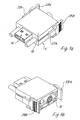
- the modular connector system comprises at least one socket part 2 (see for example Figure 3) and a plug part 4 (see for example Figure 1 or 2).
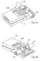
- socket part 2 and the plug part 4 with other module-like Socket or plug parts B, S if necessary, also of another design and / or function in each case in a receiving frame 42, 44, each in the connector housing 46, 48 can be inserted, which in turn can be plugged together and by means of parent locking elements 50, 52 are locked together.
- the socket part 2 and the plug part are designed according to the type of the USB standard Socket elements 12 or plug elements 14.
- the socket part and the plug part 2, 4 also each have a one or more parts closed (e.g. Fig. 1) or partially open for easier cable connection (Fig. 2) housing 16, 18, which is essentially a rectangular, flat Has shape, the grid width R of the housing 16, 18 can be designed narrow and z. B. is only 11.5 mm (see Figure 3b).
- Locking elements are located on the side walls of the housings 16, 18, respectively 20a, 20b or 22a, 22b for locking the socket and / or plug part 2.4 in one of the receiving frames 42, 44 or z. B. in a frame 24 like the figure 6 provided which, in contrast to the receiving frame of FIG. 5 individual Recordings 26 for the plug for the plug and / or socket parts 2, 4 having.
- locking elements 20, 24 according to Figure 1 or 2 each have manually operable rocker-like lugs 28a, 28b, which allow by pressing the locking elements 22a, 22b from the housing to pivot away and in this way to unlock and remove the connector part 4 on the frame.
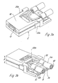
- printed circuit boards 30, 32 are parallel to the direction of insertion arranged.
- the circuit boards 30, 32 are parallel to the walls of the housing, which when inserting adjacent sockets and / or connector parts 2.4 in a frame 24 to each other or to each other.
- the printed circuit boards 30, 32 become very compact in the housing 16, 18 arranged.
- Electronic components can be placed on the printed circuit boards 32 as desired Arranged, e.g. Chokes.
- a shield support 34, 36 is located in the housing 16, 18 in each case above the printed circuit boards arranged.
- the shield support 34, 36 of the plug part 4 has one Shield bracket 38 for applying the shield 8 of the shielded cable 6c.
- the Cable cores are through the shield bracket to a terminal 40 performed, which is designed here as an example screw terminal. Alternatives are training as a terminal block is also conceivable. From the connector the cable wires with contacts of the plug and socket elements, not shown here 12, 14 connected.
- the screen support is designed such that two screens of two shielded cables 6a, 6b can be attached to the shield support. From the interaction The elements of FIGS. 1 and 3 thus result in a plug connection with T function for fieldbuses.
- the T function ensures that two cables can be connected, so that even when the plug is pulled Field device the bus is not interrupted. A field device can do so without problems be replaced. Any other signals or power connections for the field device can due to the modularity of the concept with the bus connection be connected in one plug. All other components for one Bus connectors are mandatory, can be integrated. For example, it can also be a Bus can be integrated.
- FIG. 4b 180 ° away from each other laterally out of the socket part 2.
- the screen 8 is fixed on the screen support 34, 36, for example by the shield bracket 38 or by screw terminals. But it is also conceivable to firmly connect the shielded cables 6a, 6b and 6c to the shield supports 34, 36, for example, such that a 50 cm long piece of cable from the housings 16, 18 protrudes.
- Such a variant has the advantage that none at the installation site Cable assembly must be done more on the socket and / or plug part. In this case, the interior of the housing can also be filled with a potting compound become. Potting results in increased strain relief and Vibration resistance. For example, a pre-conception with 500 mm cables conceivable, since for the bus connection of a field device often only a relatively short one Piece of cable is required.
Landscapes
- Details Of Connecting Devices For Male And Female Coupling (AREA)
- Coupling Device And Connection With Printed Circuit (AREA)
- Multi-Conductor Connections (AREA)
Abstract
Description
- Der Stecker ist geschirmt.
- Es liegen zahlreiche Labortests und Erfahrungen aus der Praxis vor, die bestätigen, daß der USB-Stecker besonders verläßlich ist. Die Anforderungen an die Steckzyklen für eine Industriesteckverbindung werden übererfüllt.
- Figur 1a/1b
- perspektivische Darstellungen eines Steckerteils eines ersten Ausführungsbeispiels der Erfindung;
- Figur 2a/2b
- perspektivische Darstellungen eines Steckerteils eines zweiten Ausführungsbeispiels der Erfindung mit teilweise offenem Gehäuse;
- Figur 3a/3b
- perspektivische Ansichten eines Buchsenteils mit teilweise offenem Gehäuse;
- Figur 4a
- ein weiteres Buchsenteil mit T-Funktion;
- Figur 4b
- das Buchsenteil aus Figur 4a in gegenüber Figur 4a gedrehter perspektivischer Darstellung;
- Figur 5
- eine Sprengansicht eines Steckverbinders; und
- Figur 6
- eine Variante eines Aufnahmerahmens.
- Buchsenteil
- 2
- Steckerteil
- 4
- abgeschirmtes Kabel
- 6, 6a, 6b
- Schirm
- 8
- Leitungsadern
- 10
- Buchsenelement
- 12
- Steckerelement
- 14a, 14b
- Gehäuse
- 16a, 14b
- Gehäuse
- 18
- Verriegelungselement
- 20a, 20b
- Verriegelungselement
- 22a, 22b
- Rahmen
- 24
- Aufnahme
- 26
- Ansatz
- 28a, 28b
- Leiterplatte
- 30
- Leiterplatte
- 32
- Schirmauflage
- 34
- Schirmauflage
- 36
- Schirmbügel
- 38
- Anschlußklemme
- 40a, 40b
- Aufnahmerahmen
- 42
- Aufnahmerahmen
- 44
- Steckergehäuse
- 46
- Steckergehäuse
- 48
- Verriegelungselemente
- 50
- Verriegelungselemente
- 52
- Buchsenteile
- B
- Steckerteile
- S
Claims (17)
- Modulares Steckverbindersystem mit wenigstens einem Buchsenteil und wenigstens Steckerteil zum Anschluß wenigstens eines abgeschirmten Kabels, wobei das Buchsenteil und/oder das Steckerteil mittels an einem Gehäuse angeordneten Verriegelungselementen jeweils modulartig in übergeordnete Aufnahmerahmen einsetzbar sind, dadurch gekennzeichnet, daß das Buchsenteil (2) und das Steckerteil (4) nach Art des USB-Standards ausgelegte Stecker- und Buchsenelemente (12, 16)aufweisen.
- Modulares Steckverbindersystem nach Anspruch 1 oder nach dem Oberbegriff des Anspruches 1, dadurch gekennzeichnet, in das Gehäuse (16, 18) eine in Einschubrichtung des Buchsen- (2) und/oder Steckerteils (4) ausgerichtete Elektronikleiterplatte (30, 32) eingebracht ist.
- Modulares Steckverbindersystem nach Anspruch 1 oder 2, dadurch gekennzeichnet, daß parallel zur Elektronikleiterplatte (30, 32) eine Schirmauflage (34, 36) zum Anschluß des Schirmes (8) des abgeschirmten Kabels (6, 6a, 6b) in das Gehäuse (16, 18) eingebracht ist.
- Modulares Steckverbindersystem nach Anspruch 3, dadurch gekennzeichnet, daß die Schirmauflage (34, 36) des Stecker- und/oder Buchsenteils wenigstens einen oder mehrere Einrichtungen zur Schirmbefestigung, insbesondere Schirmbügel (38) aufweist.
- Modulares Steckverbindersystem nach einem der vorstehenden Ansprüche, dadurch gekennzeichnet, daß die Schirmauflage (34, 36) des Stecker und/oder Buchsenteils wechselbar ausgelegt ist.
- Modulares Steckverbindersystem nach einem der vorstehenden Ansprüche, dadurch gekennzeichnet, daß das Gehäuse (16, 18) eine Rasterbreite von 11, mm aufweist.
- Modulares Steckverbindersystem nach einem der vorstehenden Ansprüche, dadurch gekennzeichnet, daß zumindest eine der Schirmauflagen (34, 36) des Stecker- und/oder Buchsenteils und die Elektronikleiterplatte (30, 32) des Stekker- (4) oder Buchsenteils (6) zur Realisierung einer T-Stückverbindung ausgelegt ist.
- Modulares Steckverbindersystem nach einem der vorstehenden Ansprüche, dadurch gekennzeichnet, daß an die Schirmauflage (34, 36) des Stecker- (4) und/oder Buchsenteils (6) zwei der abgeschirmten Kabel (6, 6a, 6b) in Einschubrichtung anschließbar sind.
- Modulares Steckverbindersystem nach einem der vorstehenden Ansprüche, dadurch gekennzeichnet, daß an die Schirmauflage (34, 36) des Stecker (4) und/oder Buchsenteils (6) zwei der abgeschirmten Kabel (6, 6a, 6b) senkrecht zur Einschubrichtung anschließbar sind.
- Modulares Steckverbindersystem nach einem der vorstehenden Ansprüche, dadurch gekennzeichnet, daß die abgeschirmten Kabel (6, 6a, 6b) an der Schirmauflage (34, 36) und/oder der Anschlußklemme (40) wechselbar befestigt sind.
- Modulares Steckverbindersystem nach einem der vorstehenden Ansprüche, dadurch gekennzeichnet, daß die abgeschirmten Kabel (6, 6a, 6b) an der Schirmauflage (34, 36) und/oder der Anschlußklemme (40) unlösbar fixiert sind.
- Modulares Steckverbindersystem nach einem der vorstehenden Ansprüche, dadurch gekennzeichnet, daß Freiräume im Stecker- und/oder Buchsengehäuse mit einer Vergußmasse ausgegossen sind.
- Modulares Steckverbindersystem nach einem der vorstehenden Ansprüche, dadurch gekennzeichnet, daß in das Gehäuse (16, 18) eine Anschlußklemme (40) zum Anschluß von Leitungsadern des abgeschirmten Kabels (6, 6a, 6b) eingebracht ist.
- Modulares Steckverbindersystem nach einem der vorstehenden Ansprüche, dadurch gekennzeichnet, daß die Anschlußklemme (40) als Schraubklemme oder als Federklemme oder IDC-Klemme ausgelegt ist.
- Modulares Steckverbindersystem nach einem der vorstehenden Ansprüche, dadurch gekennzeichnet, daß die Elektronikleiterplatte (30, 32) wenigstens eine Sperrdrossel aufweist.
- Modulares Steckverbindersystem nach einem der vorstehenden Ansprüche, dadurch gekennzeichnet, daß die Elektronikleiterplatte (30, 32) wenigstens eine schirmende Metallschicht und/oder -beschichtung aufweist.
- Modulares Steckverbindersystem nach einem der vorstehenden Ansprüche, dadurch gekennzeichnet, daß die Rastvorrichtung eine oder mehrere von Hand betätigbare Rastwippe(n) aufweist.
Applications Claiming Priority (2)
| Application Number | Priority Date | Filing Date | Title |
|---|---|---|---|
| DE20117856U | 2001-11-02 | ||
| DE20117856U DE20117856U1 (de) | 2001-11-02 | 2001-11-02 | Modulares Steckverbindersystem |
Publications (2)
| Publication Number | Publication Date |
|---|---|
| EP1309040A1 true EP1309040A1 (de) | 2003-05-07 |
| EP1309040B1 EP1309040B1 (de) | 2006-06-28 |
Family
ID=7963514
Family Applications (1)
| Application Number | Title | Priority Date | Filing Date |
|---|---|---|---|
| EP02022607A Expired - Lifetime EP1309040B1 (de) | 2001-11-02 | 2002-10-09 | Modulares Steckverbindersystem |
Country Status (4)
| Country | Link |
|---|---|
| EP (1) | EP1309040B1 (de) |
| AT (1) | ATE332021T1 (de) |
| DE (2) | DE20117856U1 (de) |
| ES (1) | ES2265469T3 (de) |
Cited By (6)
| Publication number | Priority date | Publication date | Assignee | Title |
|---|---|---|---|---|
| DE202006012687U1 (de) * | 2006-08-17 | 2007-12-27 | Weidmüller Interface GmbH & Co. KG | Modulares Steckverbindersystem |
| EP1976072A1 (de) | 2007-03-30 | 2008-10-01 | Siemens Aktiengesellschaft | Bus-Steckverbinder mit mindestens zwei Kabelanschlüssen für Busleitungen |
| WO2009146968A1 (de) * | 2008-06-06 | 2009-12-10 | Siemens Aktiengesellschaft | Stecker eines steckverbinders |
| DE202010005095U1 (de) | 2010-04-15 | 2011-08-09 | Weidmüller Interface GmbH & Co. KG | Modulares Steckverbindersystem |
| WO2020074670A1 (de) * | 2018-10-11 | 2020-04-16 | Daimler Ag | Steckeinrichtung zum laden eines energiespeichers eines kraftfahrzeugs mit elektrischer energie, kraftfahrzeug mit wenigstens einer solchen steckeinrichtung sowie ladeinfrastruktur mit wenigstens einer solchen steckeinrichtung |
| US11374348B2 (en) | 2017-03-31 | 2022-06-28 | Igus Gmbh | Modular system for plug connector modules, plug connector unit and modular housing frames for same |
Families Citing this family (3)
| Publication number | Priority date | Publication date | Assignee | Title |
|---|---|---|---|---|
| DE10355790B4 (de) * | 2003-11-26 | 2006-07-13 | Senstronic Deutschland Gmbh | Verteiler für die Automatisierung mit einem Speichermodul hierfür |
| DE102018002124A1 (de) * | 2018-03-15 | 2019-09-19 | Yamaichi Electronics Deutschland Gmbh | Steckverbinder mit Leuchtfunktion |
| DE102021117400A1 (de) | 2021-07-06 | 2023-01-12 | Harting Electric Stiftung & Co. Kg | Industriesteckverbinder mit einem Datendiodenmodul |
Citations (4)
| Publication number | Priority date | Publication date | Assignee | Title |
|---|---|---|---|---|
| CH405459A (de) * | 1963-08-05 | 1966-01-15 | Studer Draht & Kabelwerk Ag | Verfahren zur Herstellung einer permanenten Kabelverbindung und Ausrüstung zur Durchführung dieses Verfahrens |
| EP0478962A2 (de) * | 1990-10-05 | 1992-04-08 | Rohde & Schwarz GmbH & Co. KG | Mikrowellen-Streifen-Leitungsanordnung |
| DE4114921A1 (de) * | 1991-05-07 | 1992-11-12 | Ahlborn Mess Und Regelungstech | Elektrische steckverbindung |
| DE29605311U1 (de) * | 1996-03-21 | 1997-04-17 | Siemens AG, 80333 München | Vorrichtung zur Kontaktierung der Kabelschirmung eines Kabels mit einer Klemmschelle |
Family Cites Families (9)
| Publication number | Priority date | Publication date | Assignee | Title |
|---|---|---|---|---|
| DE9017670U1 (de) * | 1990-03-17 | 1991-08-14 | Licentia Patent-Verwaltungs-Gmbh, 6000 Frankfurt | Durchführung für Datenleitungen |
| DE4217205C2 (de) * | 1992-05-23 | 1994-09-08 | Amphenol Tuchel Elect | Steckverbinder |
| DE4234451C1 (de) * | 1992-10-13 | 1994-04-21 | Metz Albert Blumberger Tel | Anschlußdose für abgeschirmte Kabel, insbesondere für Datenübertragungskabel |
| US5711686A (en) * | 1996-03-01 | 1998-01-27 | Molex Incorporated | System for terminating the shield of a high speed cable |
| DE19803677B4 (de) * | 1998-01-30 | 2008-11-13 | The Whitaker Corp., Wilmington | Elektrisches Steckverbindergehäuse |
| FR2786322A1 (fr) * | 1998-09-21 | 2000-05-26 | Molex Taiwan Ltd | Connecteur electrique blinde et procede pour sa fabrication |
| DE29820771U1 (de) * | 1998-11-20 | 1999-01-14 | Weidmüller Interface GmbH & Co, 32760 Detmold | Modulares Steckverbindersystem |
| TW411044U (en) * | 1998-11-24 | 2000-11-01 | Hon Hai Prec Ind Co Ltd | Electronic connector assembly |
| TW420418U (en) * | 1999-05-15 | 2001-01-21 | Hon Hai Prec Ind Co Ltd | Electrical cable connector |
-
2001
- 2001-11-02 DE DE20117856U patent/DE20117856U1/de not_active Expired - Lifetime
-
2002
- 2002-10-09 DE DE50207370T patent/DE50207370D1/de not_active Expired - Lifetime
- 2002-10-09 EP EP02022607A patent/EP1309040B1/de not_active Expired - Lifetime
- 2002-10-09 AT AT02022607T patent/ATE332021T1/de not_active IP Right Cessation
- 2002-10-09 ES ES02022607T patent/ES2265469T3/es not_active Expired - Lifetime
Patent Citations (4)
| Publication number | Priority date | Publication date | Assignee | Title |
|---|---|---|---|---|
| CH405459A (de) * | 1963-08-05 | 1966-01-15 | Studer Draht & Kabelwerk Ag | Verfahren zur Herstellung einer permanenten Kabelverbindung und Ausrüstung zur Durchführung dieses Verfahrens |
| EP0478962A2 (de) * | 1990-10-05 | 1992-04-08 | Rohde & Schwarz GmbH & Co. KG | Mikrowellen-Streifen-Leitungsanordnung |
| DE4114921A1 (de) * | 1991-05-07 | 1992-11-12 | Ahlborn Mess Und Regelungstech | Elektrische steckverbindung |
| DE29605311U1 (de) * | 1996-03-21 | 1997-04-17 | Siemens AG, 80333 München | Vorrichtung zur Kontaktierung der Kabelschirmung eines Kabels mit einer Klemmschelle |
Cited By (9)
| Publication number | Priority date | Publication date | Assignee | Title |
|---|---|---|---|---|
| DE202006012687U1 (de) * | 2006-08-17 | 2007-12-27 | Weidmüller Interface GmbH & Co. KG | Modulares Steckverbindersystem |
| EP1976072A1 (de) | 2007-03-30 | 2008-10-01 | Siemens Aktiengesellschaft | Bus-Steckverbinder mit mindestens zwei Kabelanschlüssen für Busleitungen |
| US7604501B2 (en) | 2007-03-30 | 2009-10-20 | Siemens Aktiengesellschaft | Bus connector with at least two cable connections for bus lines |
| WO2009146968A1 (de) * | 2008-06-06 | 2009-12-10 | Siemens Aktiengesellschaft | Stecker eines steckverbinders |
| RU2442251C1 (ru) * | 2008-06-06 | 2012-02-10 | Сименс Акциенгезелльшафт | Штепсельная вилка электрического соединения |
| US8500483B2 (en) | 2008-06-06 | 2013-08-06 | Siemens Aktiengesellschaft | Plug of a plug connector |
| DE202010005095U1 (de) | 2010-04-15 | 2011-08-09 | Weidmüller Interface GmbH & Co. KG | Modulares Steckverbindersystem |
| US11374348B2 (en) | 2017-03-31 | 2022-06-28 | Igus Gmbh | Modular system for plug connector modules, plug connector unit and modular housing frames for same |
| WO2020074670A1 (de) * | 2018-10-11 | 2020-04-16 | Daimler Ag | Steckeinrichtung zum laden eines energiespeichers eines kraftfahrzeugs mit elektrischer energie, kraftfahrzeug mit wenigstens einer solchen steckeinrichtung sowie ladeinfrastruktur mit wenigstens einer solchen steckeinrichtung |
Also Published As
| Publication number | Publication date |
|---|---|
| DE50207370D1 (de) | 2006-08-10 |
| ES2265469T3 (es) | 2007-02-16 |
| ATE332021T1 (de) | 2006-07-15 |
| EP1309040B1 (de) | 2006-06-28 |
| DE20117856U1 (de) | 2003-03-13 |
Similar Documents
| Publication | Publication Date | Title |
|---|---|---|
| EP1814202B1 (de) | Kupplung | |
| DE202006006615U1 (de) | Elektronikgehäuse | |
| DE102007017571B4 (de) | Elektrisches Übergabemodul | |
| EP3164911B1 (de) | Steckverbinder | |
| EP2107648B1 (de) | Steckverbinder mit einer Schirmauflage | |
| DE102004009071B4 (de) | Elektrischer Steckverbinder | |
| DE19641440A1 (de) | Kommunikations-Auslaßdose mit niedrigem Profil | |
| EP1526612B1 (de) | Schirmanschlusseinrichtung für eine in einem Gehäuse angeordnete Leiterplatte | |
| DE10119695A1 (de) | Steckverbinder für elektronische Bauelemente | |
| EP1309040B1 (de) | Modulares Steckverbindersystem | |
| DE3239063C2 (de) | Anschlußdose für den Anschuß eines Fernsprechapparates und/oder eines oder mehrerer Fernsprech-Zusatzgeräte | |
| EP1139493B1 (de) | Elektrischer Verbinder zum Anschluss von elektrischen Leitern an ein elektrisches Gerät | |
| DE19956750B4 (de) | Steckverbinderkontakt mit Schneidanschluß | |
| DE4428687C1 (de) | Baugruppe eines elektrischen Geräts | |
| DE19830878B4 (de) | Elektrische Verbindungsanordnung zwischen zwei elektrischen Bauelementen für ein elektrisches Bauteil | |
| EP2262062B1 (de) | Steckverbinder | |
| DE19803677B4 (de) | Elektrisches Steckverbindergehäuse | |
| EP0477548A1 (de) | Steckverbindungseinrichtung für Schwachstromanlagen insbesondere der Tele- und Datenkommunikation | |
| DE202013104941U1 (de) | Elektrische Steckverbinderanordnung und Schirmanbindungselement hierzu | |
| DE202016101269U1 (de) | Klemmanschluss | |
| DE102016101271B4 (de) | Federkraftanschluss | |
| DE4238224C2 (de) | Vorrichtung zum Anschließen elektronischer Einrichtungen | |
| DE9205977U1 (de) | Mehrpoliger Kabelsteckverbinder | |
| DE102023129408A1 (de) | Anschlussadapter zum mechanischen Befestigen von elektrischen Steckverbindern verschiedener Bautypen | |
| DE102004022865B4 (de) | RJ-45-Kupplung |
Legal Events
| Date | Code | Title | Description |
|---|---|---|---|
| PUAI | Public reference made under article 153(3) epc to a published international application that has entered the european phase |
Free format text: ORIGINAL CODE: 0009012 |
|
| AK | Designated contracting states |
Designated state(s): AT BE BG CH CY CZ DE DK EE ES FI FR GB GR IE IT LI LU MC NL PT SE SK TR |
|
| AX | Request for extension of the european patent |
Extension state: AL LT LV MK RO SI |
|
| 17P | Request for examination filed |
Effective date: 20030520 |
|
| 17Q | First examination report despatched |
Effective date: 20030723 |
|
| AKX | Designation fees paid |
Designated state(s): AT BE BG CH CY CZ DE DK EE ES FI FR GB GR IE IT LI LU MC NL PT SE SK TR |
|
| GRAP | Despatch of communication of intention to grant a patent |
Free format text: ORIGINAL CODE: EPIDOSNIGR1 |
|
| GRAS | Grant fee paid |
Free format text: ORIGINAL CODE: EPIDOSNIGR3 |
|
| GRAA | (expected) grant |
Free format text: ORIGINAL CODE: 0009210 |
|
| AK | Designated contracting states |
Kind code of ref document: B1 Designated state(s): AT BE BG CH CY CZ DE DK EE ES FI FR GB GR IE IT LI LU MC NL PT SE SK TR |
|
| PG25 | Lapsed in a contracting state [announced via postgrant information from national office to epo] |
Ref country code: IT Free format text: LAPSE BECAUSE OF FAILURE TO SUBMIT A TRANSLATION OF THE DESCRIPTION OR TO PAY THE FEE WITHIN THE PRESCRIBED TIME-LIMIT;WARNING: LAPSES OF ITALIAN PATENTS WITH EFFECTIVE DATE BEFORE 2007 MAY HAVE OCCURRED AT ANY TIME BEFORE 2007. THE CORRECT EFFECTIVE DATE MAY BE DIFFERENT FROM THE ONE RECORDED. Effective date: 20060628 Ref country code: SK Free format text: LAPSE BECAUSE OF FAILURE TO SUBMIT A TRANSLATION OF THE DESCRIPTION OR TO PAY THE FEE WITHIN THE PRESCRIBED TIME-LIMIT Effective date: 20060628 Ref country code: FI Free format text: LAPSE BECAUSE OF FAILURE TO SUBMIT A TRANSLATION OF THE DESCRIPTION OR TO PAY THE FEE WITHIN THE PRESCRIBED TIME-LIMIT Effective date: 20060628 Ref country code: CZ Free format text: LAPSE BECAUSE OF FAILURE TO SUBMIT A TRANSLATION OF THE DESCRIPTION OR TO PAY THE FEE WITHIN THE PRESCRIBED TIME-LIMIT Effective date: 20060628 Ref country code: IE Free format text: LAPSE BECAUSE OF FAILURE TO SUBMIT A TRANSLATION OF THE DESCRIPTION OR TO PAY THE FEE WITHIN THE PRESCRIBED TIME-LIMIT Effective date: 20060628 Ref country code: NL Free format text: LAPSE BECAUSE OF FAILURE TO SUBMIT A TRANSLATION OF THE DESCRIPTION OR TO PAY THE FEE WITHIN THE PRESCRIBED TIME-LIMIT Effective date: 20060628 |
|
| REG | Reference to a national code |
Ref country code: GB Ref legal event code: FG4D Free format text: NOT ENGLISH |
|
| REG | Reference to a national code |
Ref country code: CH Ref legal event code: EP |
|
| REG | Reference to a national code |
Ref country code: IE Ref legal event code: FG4D Free format text: LANGUAGE OF EP DOCUMENT: GERMAN |
|
| REF | Corresponds to: |
Ref document number: 50207370 Country of ref document: DE Date of ref document: 20060810 Kind code of ref document: P |
|
| GBT | Gb: translation of ep patent filed (gb section 77(6)(a)/1977) |
Effective date: 20060731 |
|
| PG25 | Lapsed in a contracting state [announced via postgrant information from national office to epo] |
Ref country code: DK Free format text: LAPSE BECAUSE OF FAILURE TO SUBMIT A TRANSLATION OF THE DESCRIPTION OR TO PAY THE FEE WITHIN THE PRESCRIBED TIME-LIMIT Effective date: 20060928 |
|
| REG | Reference to a national code |
Ref country code: SE Ref legal event code: TRGR |
|
| PG25 | Lapsed in a contracting state [announced via postgrant information from national office to epo] |
Ref country code: CH Free format text: LAPSE BECAUSE OF NON-PAYMENT OF DUE FEES Effective date: 20061031 Ref country code: LI Free format text: LAPSE BECAUSE OF NON-PAYMENT OF DUE FEES Effective date: 20061031 Ref country code: MC Free format text: LAPSE BECAUSE OF NON-PAYMENT OF DUE FEES Effective date: 20061031 |
|
| PG25 | Lapsed in a contracting state [announced via postgrant information from national office to epo] |
Ref country code: PT Free format text: LAPSE BECAUSE OF FAILURE TO SUBMIT A TRANSLATION OF THE DESCRIPTION OR TO PAY THE FEE WITHIN THE PRESCRIBED TIME-LIMIT Effective date: 20061128 |
|
| NLV1 | Nl: lapsed or annulled due to failure to fulfill the requirements of art. 29p and 29m of the patents act | ||
| ET | Fr: translation filed | ||
| REG | Reference to a national code |
Ref country code: ES Ref legal event code: FG2A Ref document number: 2265469 Country of ref document: ES Kind code of ref document: T3 |
|
| REG | Reference to a national code |
Ref country code: IE Ref legal event code: FD4D |
|
| PLBE | No opposition filed within time limit |
Free format text: ORIGINAL CODE: 0009261 |
|
| STAA | Information on the status of an ep patent application or granted ep patent |
Free format text: STATUS: NO OPPOSITION FILED WITHIN TIME LIMIT |
|
| 26N | No opposition filed |
Effective date: 20070329 |
|
| REG | Reference to a national code |
Ref country code: CH Ref legal event code: PL |
|
| BERE | Be: lapsed |
Owner name: WEIDMULLER INTERFACE G.M.B.H. & CO. Effective date: 20061031 |
|
| PG25 | Lapsed in a contracting state [announced via postgrant information from national office to epo] |
Ref country code: AT Free format text: LAPSE BECAUSE OF NON-PAYMENT OF DUE FEES Effective date: 20061009 |
|
| PG25 | Lapsed in a contracting state [announced via postgrant information from national office to epo] |
Ref country code: GR Free format text: LAPSE BECAUSE OF FAILURE TO SUBMIT A TRANSLATION OF THE DESCRIPTION OR TO PAY THE FEE WITHIN THE PRESCRIBED TIME-LIMIT Effective date: 20060929 |
|
| PG25 | Lapsed in a contracting state [announced via postgrant information from national office to epo] |
Ref country code: BG Free format text: LAPSE BECAUSE OF FAILURE TO SUBMIT A TRANSLATION OF THE DESCRIPTION OR TO PAY THE FEE WITHIN THE PRESCRIBED TIME-LIMIT Effective date: 20060928 Ref country code: EE Free format text: LAPSE BECAUSE OF FAILURE TO SUBMIT A TRANSLATION OF THE DESCRIPTION OR TO PAY THE FEE WITHIN THE PRESCRIBED TIME-LIMIT Effective date: 20060628 |
|
| PG25 | Lapsed in a contracting state [announced via postgrant information from national office to epo] |
Ref country code: TR Free format text: LAPSE BECAUSE OF FAILURE TO SUBMIT A TRANSLATION OF THE DESCRIPTION OR TO PAY THE FEE WITHIN THE PRESCRIBED TIME-LIMIT Effective date: 20060628 Ref country code: LU Free format text: LAPSE BECAUSE OF NON-PAYMENT OF DUE FEES Effective date: 20061009 |
|
| PG25 | Lapsed in a contracting state [announced via postgrant information from national office to epo] |
Ref country code: CY Free format text: LAPSE BECAUSE OF FAILURE TO SUBMIT A TRANSLATION OF THE DESCRIPTION OR TO PAY THE FEE WITHIN THE PRESCRIBED TIME-LIMIT Effective date: 20060628 |
|
| PG25 | Lapsed in a contracting state [announced via postgrant information from national office to epo] |
Ref country code: BE Free format text: LAPSE BECAUSE OF FAILURE TO SUBMIT A TRANSLATION OF THE DESCRIPTION OR TO PAY THE FEE WITHIN THE PRESCRIBED TIME-LIMIT Effective date: 20061031 |
|
| PGFP | Annual fee paid to national office [announced via postgrant information from national office to epo] |
Ref country code: DE Payment date: 20131021 Year of fee payment: 12 Ref country code: SE Payment date: 20131022 Year of fee payment: 12 Ref country code: GB Payment date: 20131021 Year of fee payment: 12 Ref country code: FR Payment date: 20131022 Year of fee payment: 12 |
|
| PGFP | Annual fee paid to national office [announced via postgrant information from national office to epo] |
Ref country code: ES Payment date: 20131029 Year of fee payment: 12 Ref country code: IT Payment date: 20131029 Year of fee payment: 12 |
|
| REG | Reference to a national code |
Ref country code: DE Ref legal event code: R119 Ref document number: 50207370 Country of ref document: DE |
|
| REG | Reference to a national code |
Ref country code: SE Ref legal event code: EUG |
|
| GBPC | Gb: european patent ceased through non-payment of renewal fee |
Effective date: 20141009 |
|
| PG25 | Lapsed in a contracting state [announced via postgrant information from national office to epo] |
Ref country code: DE Free format text: LAPSE BECAUSE OF NON-PAYMENT OF DUE FEES Effective date: 20150501 Ref country code: SE Free format text: LAPSE BECAUSE OF NON-PAYMENT OF DUE FEES Effective date: 20141010 Ref country code: GB Free format text: LAPSE BECAUSE OF NON-PAYMENT OF DUE FEES Effective date: 20141009 |
|
| REG | Reference to a national code |
Ref country code: FR Ref legal event code: ST Effective date: 20150630 |
|
| PG25 | Lapsed in a contracting state [announced via postgrant information from national office to epo] |
Ref country code: IT Free format text: LAPSE BECAUSE OF NON-PAYMENT OF DUE FEES Effective date: 20141009 Ref country code: FR Free format text: LAPSE BECAUSE OF NON-PAYMENT OF DUE FEES Effective date: 20141031 |
|
| REG | Reference to a national code |
Ref country code: ES Ref legal event code: FD2A Effective date: 20151126 |
|
| PG25 | Lapsed in a contracting state [announced via postgrant information from national office to epo] |
Ref country code: ES Free format text: LAPSE BECAUSE OF NON-PAYMENT OF DUE FEES Effective date: 20141010 |