EP1349264B1 - Basisstufe für Ladungspumpeschaltung - Google Patents
Basisstufe für Ladungspumpeschaltung Download PDFInfo
- Publication number
- EP1349264B1 EP1349264B1 EP02425199A EP02425199A EP1349264B1 EP 1349264 B1 EP1349264 B1 EP 1349264B1 EP 02425199 A EP02425199 A EP 02425199A EP 02425199 A EP02425199 A EP 02425199A EP 1349264 B1 EP1349264 B1 EP 1349264B1
- Authority
- EP
- European Patent Office
- Prior art keywords
- transistors
- biasing
- inverters
- charge pump
- terminals
- Prior art date
- Legal status (The legal status is an assumption and is not a legal conclusion. Google has not performed a legal analysis and makes no representation as to the accuracy of the status listed.)
- Expired - Lifetime
Links
- 239000003990 capacitor Substances 0.000 claims description 14
- 238000005516 engineering process Methods 0.000 claims description 8
- 230000000295 complement effect Effects 0.000 claims description 4
- 230000006870 function Effects 0.000 description 5
- 230000015654 memory Effects 0.000 description 3
- 239000000758 substrate Substances 0.000 description 3
- 239000002184 metal Substances 0.000 description 2
- 230000003247 decreasing effect Effects 0.000 description 1
- 230000000694 effects Effects 0.000 description 1
- 230000003071 parasitic effect Effects 0.000 description 1
- 239000004065 semiconductor Substances 0.000 description 1
- 239000000126 substance Substances 0.000 description 1
Images


Classifications
-
- H—ELECTRICITY
- H02—GENERATION; CONVERSION OR DISTRIBUTION OF ELECTRIC POWER
- H02M—APPARATUS FOR CONVERSION BETWEEN AC AND AC, BETWEEN AC AND DC, OR BETWEEN DC AND DC, AND FOR USE WITH MAINS OR SIMILAR POWER SUPPLY SYSTEMS; CONVERSION OF DC OR AC INPUT POWER INTO SURGE OUTPUT POWER; CONTROL OR REGULATION THEREOF
- H02M3/00—Conversion of DC power input into DC power output
- H02M3/02—Conversion of DC power input into DC power output without intermediate conversion into AC
- H02M3/04—Conversion of DC power input into DC power output without intermediate conversion into AC by static converters
- H02M3/06—Conversion of DC power input into DC power output without intermediate conversion into AC by static converters using resistors or capacitors, e.g. potential divider
- H02M3/07—Conversion of DC power input into DC power output without intermediate conversion into AC by static converters using resistors or capacitors, e.g. potential divider using capacitors charged and discharged alternately by semiconductor devices with control electrode, e.g. charge pumps
- H02M3/073—Charge pumps of the Schenkel-type
-
- G—PHYSICS
- G11—INFORMATION STORAGE
- G11C—STATIC STORES
- G11C5/00—Details of stores covered by group G11C11/00
- G11C5/14—Power supply arrangements, e.g. power down, chip selection or deselection, layout of wirings or power grids, or multiple supply levels
- G11C5/145—Applications of charge pumps; Boosted voltage circuits; Clamp circuits therefor
-
- H—ELECTRICITY
- H02—GENERATION; CONVERSION OR DISTRIBUTION OF ELECTRIC POWER
- H02M—APPARATUS FOR CONVERSION BETWEEN AC AND AC, BETWEEN AC AND DC, OR BETWEEN DC AND DC, AND FOR USE WITH MAINS OR SIMILAR POWER SUPPLY SYSTEMS; CONVERSION OF DC OR AC INPUT POWER INTO SURGE OUTPUT POWER; CONTROL OR REGULATION THEREOF
- H02M3/00—Conversion of DC power input into DC power output
- H02M3/02—Conversion of DC power input into DC power output without intermediate conversion into AC
- H02M3/04—Conversion of DC power input into DC power output without intermediate conversion into AC by static converters
- H02M3/06—Conversion of DC power input into DC power output without intermediate conversion into AC by static converters using resistors or capacitors, e.g. potential divider
- H02M3/07—Conversion of DC power input into DC power output without intermediate conversion into AC by static converters using resistors or capacitors, e.g. potential divider using capacitors charged and discharged alternately by semiconductor devices with control electrode, e.g. charge pumps
- H02M3/071—Conversion of DC power input into DC power output without intermediate conversion into AC by static converters using resistors or capacitors, e.g. potential divider using capacitors charged and discharged alternately by semiconductor devices with control electrode, e.g. charge pumps adapted to generate a negative voltage output from a positive voltage source
Definitions
- the present invention relates to a basic stage for a charge pump circuit.
- the invention relates to a basic stage for a charge pump circuit having at least an input terminal and an output terminal, and comprising:
- the invention relates particularly, but not exclusively, to a charge pump circuit for generating positive and negative voltages suitable for use in non volatile memory devices and the following description is made with reference to this field of application for convenience of illustration only.
- semiconductor non volatile memories such as EPROM, EEPROM and Flash memories, require for the correct operation thereof voltage values which are higher than a supply voltage reference VDD, and lower than a ground voltage reference GND.
- the erasing operation of a non volatile memory requires a positive overvoltage equal to about 10V as well as a negative overvoltage equal to -8V, both generated from a supply voltage reference ranging between 1.8V and 5V and a ground voltage reference GND, that is conventionally equal to 0V.
- charge pump circuits To generate these positive and negative overvoltages charge pump circuits are presently used. These circuits are generally realised by cascading a plurality of basic stages.
- the most known charge pump circuit is the so-called four-phase charge pump circuit, comprising a cascade of N driven basic stages, each one being driven by the two phases of a clock signal CK and ⁇ CK.
- CK and ⁇ CK For the correct operation of such a circuit, two consecutive basic stages must be driven by different phases and thus four phases are required to drive the whole charge pump circuit.
- a basic stage for a known charge pump circuit is schematically shown in figure 1, globally indicated with 1.
- the basic stage 1 has an input terminal IN connected to the input terminal of the charge pump circuit, if it is the first stage, or to an output terminal of a previous stage, as well as an output terminal connected to an input terminal of a following stage or to the output terminal of the charge pump circuit, if it is the last stage.
- the basic stage 1 comprises a first M1 and second M2 MOS transistors of the N-channel type having the conduction terminals connected to said input terminal IN and to a first C1 and second C2 capacitors in correspondence with an internal circuit node X and of the output terminal OUT respectively.
- the transistors M1 and M2 have also the control terminals cross-connected to the output terminal OUT and to the internal circuit node X respectively.
- the basic stage 1 has also a first CK and second ⁇ CK driving signals applied to the capacitors C1 and C2, these driving signals being one opposite to the other.
- the second capacitor C2 is used for the charge transfer performed by the basic stage 1, the first capacitor C1 aiming only at generating a high overdrive voltage during the charging of the second capacitor C2.
- the transistors used in the known charge pump circuits are usually of the "High Voltage” type since they must support a voltage being twice the circuit supply voltage VDD, applied to the control terminal thereof in particular operating conditions.
- the cascade structure of a charge pump circuit using basic stages like the stage 1 is schematically shown in figure 2 and globally indicated with 2.
- the charge pump circuit 2 comprises a plurality of basic stages S1, S2, ..., SN, each stage having the structure shown in figure 1.
- the charge pump circuit 2 uses four driving signals A, ⁇ A, B and ⁇ B suitable to ensure a constant output power supply.
- they are step signals with different phases as shown in figure 3: it is thus impossible to use too high frequencies since there is the risk to loose the right correlation required for the correct operation of the charge pump circuit 2.
- the charge pump circuit 2 also requires a further output stage to reduce the ripple at the output terminal OUT of the last stage SN.
- the charge pump circuit according to these documents comprises a plurality of basic stages as the one schematically shown in figure 4 and globally indicated with 3.
- the basic stage 3 has a first node UP corresponding to the highest voltage node and a second node DOWN corresponding to the lowest voltage node.
- the node UP can be connected to the output terminal of a charge pump circuit comprising the basic stage 3 or to the input terminal of a following stage, while the node DOWN can be connected to a supply reference or to an output terminal of a previous stage.
- the basic stage 3 comprises a first MP1 and second MP2 MOS transistors of the P-channel type, having the conduction terminals connected to the node UP and to a first XL and second XR internal circuit nodes respectively.
- the basic stage 3 also comprises a third MN 1 and a fourth MN2 MOS transistors of the N-channel type, having the conduction terminals connected to the internal circuit nodes XL and XR respectively, and to the node DOWN.
- the first MP1 and third MN1 transistors realise a first inverter inserted between the nodes UP and DOWN and having the first internal circuit node XL as central point.
- the second MP2 and the fourth MN2 transistors realise a second inverter inserted between the nodes UP and DOWN and having the second internal circuit node XR as central point.
- the first transistor MP1 also has the control terminal connected to the control terminal of the third transistor MN1 as well as to the second internal circuit node XR.
- the second transistor MP2 also has the control terminal connected to the control terminal of the fourth transistor MN2 as well as to the first internal circuit node XL.
- the first and second transistors MP1 and MP2 also have the bulk terminals connected to the node UP, while the third MN1 and the fourth MN2 transistors have the bulk terminals connected to the node DOWN.
- the basic stage 3 also comprises a first CL and second CR capacitors connected to the nodes XL and XR respectively, and receiving a first CK and second CK_N driving signals.
- the PMOS transistors MP1 and MP2 have the function of multiplexing the voltage values at the nodes XL and XR, connecting the highest voltage value node to the node UP.
- the charge pump circuit obtained through a cascade of basic stages like the stage 3 requires only two driving signals and it is referred to as two-phase charge pump circuit. This allows higher frequencies to be used for these signals without risking to loose the synchronism of the basic stage cascade.
- Such a two-phase charge pump circuit has a voltage value which is substantially constant at the output terminal (corresponding to the node UP of the last cascade stage).
- the output voltage stability allows Low Voltage transistors to be used, these transistors having lower size and greater conductivity characteristics with respect to the High Voltage transistors used in the four-phase charge pump circuits.
- Suitable arrangements must therefore be provided in the layout phase of the charge pump circuit to avoid such a latch-up phenomenon.
- the technical problem underlying the present invention is to provide a basic stage for a charge pump circuit, having such structural and functional characteristics as to avoid latch-up phenomena, allowing in the meanwhile a negative charge pump circuit to be realised and thus overcoming the limits of the charge pump circuits according to the prior art.
- the solutive idea underlying the present invention is to bias in a suitable way the bulk terminals of the transistors comprised in each basic stage of the charge pump circuit to avoid any forward bias of the junctions thereof, thus obtaining a unique layout for positive and negative charge pump circuits.
- the basic stage 10 has a first node UP corresponding to the highest voltage node and a second node DOWN corresponding to the lowest voltage node.
- the node UP can be connected to the output terminal of a charge pump circuit comprising the basic stage 3 or to the input terminal of a following stage, while the node DOWN can be connected to a supply reference or to an output terminal of a previous stage.
- the basic stage 10 comprises a first MP1 and second MP2 MOS transistors of the P-channcl type, having the conduction terminals connected to the node UP and to a first XL and second XR internal circuit nodes respectively.
- the basic stage 10 also comprises a third MN 1 and fourth MN2 MOS transistors of the N-channel type, having the conduction terminals connected to the internal circuit nodes XL and XR respectively and to the node DOWN.
- the first MP1 and third MN1 transistors realise a first inverter inserted between the nodes UP and DOWN and having the first internal circuit node XL as central point.
- the second MP2 and fourth MN2 transistors realise a second inverter inserted between the nodes UP and DOWN and having the second internal circuit node XR as central point.
- the first transistor MP1 also has the control terminal connected to the control terminal of the third transistor MN1 as well as to the second internal circuit node XR.
- the second transistor MP2 also has the control terminal connected to the control terminal of the fourth transistor MN2 as well as to the first internal circuit node XL.
- the transistors MP1 and MP2 select the highest voltage node between the first XL and second XR internal circuit nodes and they connect it to the node UP, while the transistors MN1 and MN2 select the lowest voltage node between the first XL and second XR internal circuit nodes and they connect it to the node DOWN.
- the basic stage 10 comprises also a first CL and second CR capacitors connected to the nodes XL and XR respectively and receiving a first CK and second CK_N driving signals.
- the second driving signal CR_N is the logic negation of the first driving signal CK.
- the basic stage 10 also comprises a first biasing structure 11 connected to the control terminals of the PMOS transistors MP1 and MP2, as well as to the internal circuit nodes XL and XR.
- the first biasing structure 11 comprises a first MOS biasing transistor MP3 of the P-channel type, having a control terminal connected to the control terminal of the first transistor MP1, as well as a drain terminal connected to the first internal circuit node XL. Further, the first biasing transistor MP3 receives a first biasing signal BP at the source and bulk terminals thereof, the signal BP being also applied to the bulk terminal of the first transistor MP1.
- the first biasing structure 11 comprises a second MOS biasing transistor MP4 of the P-channel type, having a control terminal connected to the control terminal of the second transistor MP2, as well as a drain terminal connected to the second internal circuit node XR. Further, the second biasing transistor MP4 receives a first biasing signal BP on the source and bulk terminals thereof, the signal BP being also applied to the bulk terminal of the second transistor MP2.
- the first biasing structure 11 comprises transistors MP3 and MP4 having far smaller size with respect to the size of the transistors MP1 and MP2 of the basic stage 10 of the charge pump. Substantially, the first biasing structure 11 has the same function as the transistors MP1 and MP2, i.e. it selects the highest voltage node between the first XL and second XR internal circuit nodes and connects such a highest voltage node to the bulk terminals of the PMOS transistors, forcing the value of the first biasing signal BP.
- the node UP of the basic stage 10 is the input of a following stage in the charge pump circuit and it is necessarily a high-value capacitive load, while the bulk terminals of the PMOS transistors are connected only to the NWELL wherein those transistors are realised.
- the forward bias of the junctions p+/NWELL of the transistors MP3 and MP4 occurs with far lower currents than the current of the known structure comprising only the transistors MP1, MP2, MN1 and MN2.
- the quantity of current involved in that junction is proportional to the ratio between the capacities among which the charge is reassessed and the capacity of the NWELL with respect to the capacitors CL and CR of the basic stage of the charge pump is lower by two orders of magnitude.
- the transistors MP3 and MP4 of the first biasing structure 11 force the node UP to the highest voltage value at the internal circuit nodes XL and XR in advance with respect to the transistors MP1 and MP2 of the basic stage 10 of the charge pump.
- the basic stage 10 also comprises a second biasing structure 12 connected to the control terminals of the NMOS transistors MN1 and MN2, as well as to the internal circuit nodes XL and XR.
- the second biasing structure 12 comprises a third MOS biasing transistor MN3 of the N-channel type, having a control terminal connected to the control terminal of the third transistor MN1, as well as a drain terminal connected to the first internal circuit node XL. Further, the third biasing transistor MN3 receives a second biasing signal BN on the source and bulk terminals thereof, the signal BN being also applied to the bulk terminal of the third transistor MN1.
- the second biasing structure 12 comprises a fourth MOS biasing transistor MN4 of the N-channel type, having a control terminal connected to the control terminal of the fourth transistor MN2, as well as a drain terminal connected to the second internal circuit node XR. Further, the fourth biasing transistor MN4 receives the second biasing signal BN on the source and bulk terminals thereof, the signal BN being also applied to the bulk terminal of the fourth transistor MN2.
- the second biasing structure 12 comprises transistors MN3 and MN4 having far smaller size with respect to the size of the transistors MN1 and MN2 of the basic stage 10 of the charge pump.
- the second biasing structure 12 has the same function as the transistors MN1 and MN2, i.e. it selects the lowest voltage node between the first XL and second XR internal circuit nodes and it connects such lowest voltage node to the bulk terminals of the NMOS transistors, forcing the value of the second biasing signal BN.
- the node DOWN of the basic stage 10 is the input of a previous stage in the charge pump circuit and it is necessarily a high-value capacitive load, while the bulk terminals of the NMOS transistors are connected only to the PWELL wherein those transistors are realised.
- the forward bias of the junctions N+/PWELL of the transistors MN3 and MN4 occurs with very lower currents than the current of the known structure comprising only the transistors MP1, MP2, MN1 and MN2.
- the quantity of current involved in that junction is proportional to the ratio between the capacities among which the charge is reassessed and the capacity of the PWELL with respect to the capacitors CL and CR of the basic stage of the charge pump is lower by two orders of magnitude.
- the transistors MN3 and MN4 of the second biasing structure 12 force the node DOWN to the lowest voltage value at the internal circuit nodes XL and XR in advance with respect to the transistors MN1 and MN2 of the basic stage 10 of the charge pump.
- the NMOS transistors are realised in a triple-well technology and they have a first bulk terminal corresponding to the PWELL and a second well terminal corresponding to the NWELL of the triple-well structure, represented in the figure as connected to the bulk terminal by means of respective diodes D1, D2, D3 and D4.
- the biasing of the NWELL and PWELL is not provided by outer signals, but it is generated in each basic stage (signals BP and BN) or it is forced to the voltage references VDD and GND.
- the first driving signal CK is at a high logic value
- the first internal circuit node XL is at a highest voltage value: thus, that first node XL corresponds to the source terminal of the first transistor MP1 and of the first biasing transistor MP3.
- the second internal circuit node XR is, on the contrary, at a lower potential since it is driven by the second driving signal CK_N, which is the negation of the first driving signal CK.
- the first biasing signal BP brings the bulk terminals of the PMOS transistors MP1, MP2, MP3 and MP4 at a higher potential value avoiding the forward bias of the junctions P+/Nwell of such transistors.
- the second transistor MP2 is off, the control and source terminals thereof being at the same potential.
- the first internal circuit node XL is at the lowest voltage value: that first node XL corresponds to the source terminal of the third transistor MN1 and of the third biasing transistor MN3.
- the second internal circuit node XR is at a higher potential since it is driven by the second driving signal CK_N, which is the negation of the first driving signal CK.
- the second biasing signal BN brings the bulk and well terminals of the NMOS transistors MN1, MN2, MN3 and MN4 at a lower potential value, thereby avoiding the forward bias of the junctions N+/Pwell of such transistors.
- the fourth biasing transistor MN2 is off, the control and source terminals thereof being at the same potential.
- the described basic stage 10 is thus used to realise a positive charge pump circuit, forcing the bulk terminals of the transistors MP1, MP2, MP3 and MP4, corresponding to a single contact NWELL of all the PMOS transistors, to the value of the first biasing signal BP, forcing the bulk terminals of the transistors MN1, MN2, MN3 and MN4, corresponding to a single contact PWELL of all the NMOS transistors of each basic stage, to the value of the second biasing signal BN and forcing the terminal NWELL of the triple-WELL structure, wherein the NMOS transistors are realised, to the value of the second biasing signal BN.
- the P-type substrate is also ground-biased.
- biasing structures 11 and 12 are self-consistent and they achieve the function
- the scheme of Figure 6 takes into account voltage values Y higher than 0V, owing to the biasing of the wells Nwell of the PMOS transistors MP1 and MP2.
- the voltage values Z have no limitations for the well-known and widely-used triple-well NMOS technologies provided that, for negative voltage values Z, the Nwell and Pwell terminals of the stage 10 are connected to each other.
- the basic stage 10 is used also to realise a charge pump circuit for a negative voltage.
- the NWELL of the triple-well structure wherein the NMOS transistors are realised, is connected to the supply voltage reference VDD (and it does not receive the second biasing signal BN anymore, as seen for the positive pump basic stage). Therefore, the terminal of the PWELL wherein the NMOS transistors are realised can be brought to negative voltages without bringing the NWELL containing it underground, since it is separately biased at a no negative potential value (in the example shown, the supply voltage reference VDD).
- the highest voltage value at the nodes XL and XR varies from the negative supply voltage value (-VDD) and a value u which is certainly positive and lower than the positive supply voltage value VDD, ensuring the correct biasing of that NWELL.
- Such a basic stage 10 represents a charge pump circuit having only one stage.
- the first basic stage to be used in such a chain has the bulk terminals of the PMOS transistors, corresponding to the only terminal of the NWELL wherein they are realised, biased through the first biasing signal BP, the bulk terminals of the NMOS transistors, corresponding to the terminal of the PWELL wherein they are realised, biased through the second biasing signal BN and the terminal of the well NWELL of the triple-well structure wherein they are realised the NMOS transistors connected to the supply voltage reference VDD.
- the P-type substrate is still ground-biased.
- the basic stages following the first one in the chain composing the negative pump circuit have, on the contrary, the bulk terminals of the PMOS transistors, corresponding to the single terminal of the NWELL wherein they are realised, biased to ground GND.
- the output voltage of the previous stages in the chain is certainly negative and the structure for biasing the bulk terminals of the PMOS transistors cannot be used since the NWELL containing them cannot be biased at negative voltage values which would direct-connect the parasitic diode NWELL/P-type substrate (always connected to the ground reference GND).
- biasing transistors MP3 and MP4 loose their function.
- these transistors MP3 and MP4 are parallel-connected to the transistors MP1 and MP2 of the charge pump basic stage.
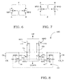
- biasing structure 11 comprising the transistors MP3 and MP4 taking into consideration a basic stage 100 having only one biasing structure for the NMOS transistors, as schematically shown in figure 8.
- the basic stage 100 comprises a biasing structure 120 comprising MOS biasing transistors MN3 and MN4 of the N-channel type, which are connected in the same way as the biasing transistors of the biasing structure 12 of figure 5.
- the well terminals of the biasing transistors MN3 and MN4 are connected to the supply voltage reference VDD.
- the basic stage 100 provides that the bulk terminals of the transistors MP1 and MP2 are connected to the ground GND, eliminating the need to use a biasing structure 11 for those PMOS transistors. In that case, it is necessary to use High Voltage PMOS transistors. It should be noted that the basic stage 100, except for the depletion effect on the transistors MP1 and MP2 which is inevitable if PMOS transistors are used, still shows the following advantages:
Landscapes
- Engineering & Computer Science (AREA)
- Power Engineering (AREA)
- Semiconductor Integrated Circuits (AREA)
- Dc-Dc Converters (AREA)
- Electronic Switches (AREA)
Claims (12)
- Basisstufe für eine Ladungspumpenschaltung mit mindestens einem Eingangsanschluss (UP) und einem Ausgangsanschluss (DOWN) und umfassend:wobei der erste Vorspann-Transistor (MN3) mit einem Steueranschluss versehen ist, der mit dem zweiten internen Knoten (XR) verbunden ist, sowie mit einem Abflussanschluss (drain terminal) versehen ist, der mit dem ersten internen Knoten (XL) verbunden ist, und der zweite Vorspann-Transistor (MN4) mit einem Steueranschluss versehen ist, der mit dem ersten internen Knoten (XL) verbunden ist, sowie mit einem Abflussanschluss versehen ist, der mit dem zweiten internen Knoten (XR) verbunden ist;mindestens einen ersten Wechselrichter, der zwischen den Eingangs- und Ausgangsanschlüssen (UP, DOWN) eingefügt ist, und umfassend ein erstes komplementäres Paar von Transistoren (MP1, MN1), die einen ersten internen Knoten (XL) definieren,mindestens einen zweiten Wechselrichter, der zwischen den Eingangs- und Ausgangsanschlüssen (UP, DOWN) eingefügt ist, und umfassend ein zweites komplementäres Paar von Transistoren (MP2, MN2), die einen zweiten internen Knoten (XR) definieren, wobei die ersten (MP1, MN1) und zweiten (MP2, MN2) Paare von Transistoren ihre Steueranschlüsse über Kreuz mit den zweiten (XR) und den ersten (XL) internen Knoten verbunden haben,einzelne erste und zweite Kondensatoren (CL, CR), die an den ersten und zweiten internen Knoten (XL, XR) angeschlossen sind und erste und zweite Ansteuersignale (CK, CK_N) empfangen;mindestens eine erste Vorspann-Anordnung (12), die mit den ersten und zweiten internen Knoten (XL, XR) verbunden ist und einen ersten (MN3) und einen zweiten (MN4) Vorspann-Transistor umfasst, die jeweils mit dem ersten und zweiten Wechselrichter gekoppelt sind,
dadurch gekennzeichnet, dass der erste und zweite Vorspann-Transistor (MN3, MN4) und die ersten Transistoren (MN1, MN2) der ersten und zweiten Wechselrichter in der Dreiwannentechnologie (triple-well technology) realisiert sind und Wannenanschlüsse haben, die von den Substratanschlüssen (bulk terminals) verschieden sind. - Basisstufe nach Anspruch 1, dadurch gekennzeichnet, dass diese eine zweite Vorspann-Anordnung (11) aufweist, die mit den ersten und zweiten internen Knoten (XL, XR) verbunden ist und einen dritten (MP3) und vierten Vorspann-Transistor (MP4) umfasst, die jeweilig mit dem ersten und zweiten Wechselrichter verbunden sind.
- Basisstufe nach Anspruch 2, dadurch gekennzeichnet, dass der dritte Vorspann-Transistor (MP3) einen Steueranschluss, der mit dem zweiten internen Knoten (XR) verbunden ist, sowie einen Abflussanschluss hat, der mit dem ersten internen Knoten (XL) verbunden ist, und dass der vierte Vorspann-Transistor (MP4) einen Steueranschluss, der mit dem ersten internen Knoten (XL) verbunden ist, sowie einen Abflussanschluss hat, der mit dem zweiten internen Knoten (XR) verbunden ist.
- Basisstufe nach einem der Ansprüche 1 bis 3, dadurch gekennzeichnet, dass die ersten und zweiten Vorspann-Transistoren (MN3, MN4) und die ersten Transistoren (MN1, MN2) der ersten und zweiten Wechselrichter n-Kanal-leitende MOS-Transistoren sind.
- Basisstufe nach einem der Ansprüche 1 bis 3, dadurch gekennzeichnet, dass die dritten und vierten Vorspann-Transistoren (MP4, MP4) und die zweiten Transistoren (MP1, MP2) der ersten und zweiten Wechselrichter p-Kanal leitende MOS-Transistoren sind.
- Basisstufe nach einem der vorhergehenden Ansprüche, dadurch gekennzeichnet, dass die ersten und zweiten Vorspann-Transistoren (MN3, MN4) und die ersten Transistoren (MN1 und MN2) der ersten und zweiten Wechselrichter Niederspannungstransistoren sind.
- Basisstufe nach einem der vorhergehenden Ansprüche, dadurch gekennzeichnet, dass die ersten und zweiten Transistoren (MP1, MP2) Hochspannungstransistoren sind.
- Basisstufe nach einem der Ansprüche 1 bis 7, dadurch gekennzeichnet, dass diese für eine positive Ladungspumpenschaltung konfiguriert ist, die die Substratanschlüsse der ersten und zweiten Vorspann-Transistoren (MN3, MN4) und der ersten Transistoren (MN1, MN2) der ersten und zweiten Wechselrichter auf ein gleiches erstes Vorspann-Signal (BN) treibt, die Substratanschlüsse der dritten und vierten Vorspann-Transistoren (MP3, MP4) und der zweiten Transistoren (MP1, MP2) der ersten und zweiten Wechselrichter auf ein gleiches zweites Vorspann-Signal (BP) treibt und die Wannenanschlüsse der ersten und zweiten Vorspann-Transistoren (MN3, MN4) und ersten Transistoren (MN1, MN2) der ersten und zweiten Wechselrichter, die in einer Dreiwannentechnologie realisiert sind auf das erste Vorspann-Signal (BN) treibt.
- Basisstufe nach einem der Ansprüche 1 bis 7, dadurch gekennzeichnet, dass diese für eine negative Ladungspumpenschaltung konfiguriert ist, die die Substratanschlüsse der ersten und zweiten Vorspann-Transistoren (MN3, MN4) und der ersten Transistoren (MN1, MN2) der ersten und zweiten Wechselrichter auf ein gleiches erstes Vorspann-Signal (BN) treibt, die Substratanschlüsse der dritten und vierten Vorspann-Transistoren (MP3, MP4) und der zweiten Transistoren (MP1, MP2) der ersten und zweiten Wechselrichter auf ein gleiches zweites Vorspann-Signal (BP) treibt und die Wannenanschlüsse der ersten und zweiten Vorspann-Transistoren (MN3, MN4) und der ersten Transistoren (MN1, MN2) der ersten und zweiten Wechselrichter, die in der Dreiwannentechnologie realisiert sind, auf eine Versorgungs-Bezugsspannung (VDD) treibt.
- Basisstufe nach einem der Ansprüche 1 bis 7, dadurch gekennzeichnet, dass diese für eine negative Ladungspumpenschaltung konfiguriert ist, die Substratanschlüsse der ersten und zweiten Vorspann-Transistoren (MN3, MN4) und der ersten Transistoren (MN1, MN2) der ersten und zweiten Wechselrichter auf ein gleiches erstes Vorspann-Signal (BN) treibt, die Substratanschlüsse der dritten und vierten Vorspannungs-Transistoren (MP3, MP4) und der zweiten Transistoren (MP1, MP2) der ersten und zweiten Wechselrichter auf eine Bezugserdspannung (GND) treibt und die Wannenanschlüsse der ersten und zweiten Vorspann-Transistoren (MN3, MN4) und der ersten Transistoren (MN1, MN2) der ersten und zweiten Wechselrichter, die in einer Dreiwannentechnologie realisiert sind, auf eine Versorgungs-Bezugsspannung (VDD) treibt.
- Positive Ladungspumpenschaltung umfassend eine Vielzahl von Basisstufen in Kaskadenschaltung, dadurch gekennzeichnet, dass jede der Basisstufen nach Anspruch 8 realisiert ist.
- Negative Ladungspumpenschaltung umfassend eine Vielzahl von Basisstufen in Kaskadenschaltung, dadurch gekennzeichnet, dass diese mindestens eine erste Basisstufe realisiert nach Anspruch 10 und eine Vielzahl von Basisstufen in Kaskadenschaltung realisiert nach Anspruch 9 umfasst.
Priority Applications (3)
| Application Number | Priority Date | Filing Date | Title |
|---|---|---|---|
| DE60207190T DE60207190D1 (de) | 2002-03-29 | 2002-03-29 | Basisstufe für Ladungspumpeschaltung |
| EP02425199A EP1349264B1 (de) | 2002-03-29 | 2002-03-29 | Basisstufe für Ladungspumpeschaltung |
| US10/402,852 US7002399B2 (en) | 2002-03-29 | 2003-03-28 | Basic stage for a charge pump circuit |
Applications Claiming Priority (1)
| Application Number | Priority Date | Filing Date | Title |
|---|---|---|---|
| EP02425199A EP1349264B1 (de) | 2002-03-29 | 2002-03-29 | Basisstufe für Ladungspumpeschaltung |
Publications (2)
| Publication Number | Publication Date |
|---|---|
| EP1349264A1 EP1349264A1 (de) | 2003-10-01 |
| EP1349264B1 true EP1349264B1 (de) | 2005-11-09 |
Family
ID=27798973
Family Applications (1)
| Application Number | Title | Priority Date | Filing Date |
|---|---|---|---|
| EP02425199A Expired - Lifetime EP1349264B1 (de) | 2002-03-29 | 2002-03-29 | Basisstufe für Ladungspumpeschaltung |
Country Status (3)
| Country | Link |
|---|---|
| US (1) | US7002399B2 (de) |
| EP (1) | EP1349264B1 (de) |
| DE (1) | DE60207190D1 (de) |
Cited By (1)
| Publication number | Priority date | Publication date | Assignee | Title |
|---|---|---|---|---|
| CN109164866A (zh) * | 2018-08-31 | 2019-01-08 | 南方科技大学 | 基于负电荷泵增强的低压差线性稳压器和电源管理芯片 |
Families Citing this family (14)
| Publication number | Priority date | Publication date | Assignee | Title |
|---|---|---|---|---|
| FR2884072A1 (fr) * | 2005-04-01 | 2006-10-06 | St Microelectronics Sa | Procede de controle du fonctionnement d'une pompe de charge et circuit integre de pompe de charge correspondant |
| US20070109035A1 (en) * | 2005-11-16 | 2007-05-17 | Michael Tsivyan | Charge pump |
| US20080068068A1 (en) * | 2006-09-19 | 2008-03-20 | Sridhar Yadala | Method and system for charge pumps |
| KR100909837B1 (ko) | 2007-08-14 | 2009-07-28 | 창원대학교 산학협력단 | 단위전하펌프 |
| KR100926677B1 (ko) | 2007-08-14 | 2009-11-17 | 창원대학교 산학협력단 | 단위전하펌프 |
| US8847671B2 (en) | 2009-09-01 | 2014-09-30 | Aptus Power Semiconductor | Methods and circuits for a low input voltage charge pump |
| US8441307B2 (en) * | 2009-09-01 | 2013-05-14 | Aptus Power Semiconductor | Methods and circuits for a low input voltage charge pump |
| US9026063B2 (en) * | 2011-05-17 | 2015-05-05 | Triquint Semiconductor, Inc. | Complementary metal-oxide semiconductor direct current to direct current converter |
| US9379103B2 (en) * | 2012-10-17 | 2016-06-28 | Semtech Corporation | Semiconductor device and method of preventing latch-up in a charge pump circuit |
| US10365833B2 (en) | 2016-01-22 | 2019-07-30 | Micron Technology, Inc. | Apparatuses and methods for encoding and decoding of signal lines for multi-level communication architectures |
| US10283187B2 (en) * | 2017-07-19 | 2019-05-07 | Micron Technology, Inc. | Apparatuses and methods for providing additional drive to multilevel signals representing data |
| US10461636B2 (en) * | 2017-10-23 | 2019-10-29 | Stmicroelectronics International N.V. | Voltage multiplier circuit with a common bulk and configured for positive and negative voltage generation |
| CN111490664B (zh) * | 2019-01-29 | 2021-07-06 | 合肥格易集成电路有限公司 | 一种驱动电路 |
| US11031865B2 (en) | 2019-08-12 | 2021-06-08 | Stmicroelectronics International N.V. | Charge pump circuit configured for positive and negative voltage generation |
Family Cites Families (11)
| Publication number | Priority date | Publication date | Assignee | Title |
|---|---|---|---|---|
| CH593510B5 (de) * | 1975-08-14 | 1977-12-15 | Ebauches Sa | |
| JP2805991B2 (ja) * | 1990-06-25 | 1998-09-30 | ソニー株式会社 | 基板バイアス発生回路 |
| DE69408665T2 (de) * | 1994-08-12 | 1998-10-15 | Cons Ric Microelettronica | Spannungserhöher vom Ladungspumpentype |
| US6100557A (en) * | 1996-10-10 | 2000-08-08 | Macronix International Co., Ltd. | Triple well charge pump |
| JP4026947B2 (ja) * | 1998-08-24 | 2007-12-26 | 株式会社ルネサステクノロジ | 昇圧回路 |
| US6252429B1 (en) * | 1999-05-24 | 2001-06-26 | International Business Machines Corporation | Method and apparatus for improving device matching and switching point tolerance in silicon-on-insulator cross-coupled circuits |
| FR2794301B1 (fr) * | 1999-05-28 | 2004-10-08 | St Microelectronics Sa | Procede de multiplication de tension, et dispositif multiplicateur de tension correspondant |
| US6429723B1 (en) * | 1999-11-18 | 2002-08-06 | Texas Instruments Incorporated | Integrated circuit with charge pump and method |
| TW486869B (en) * | 1999-12-27 | 2002-05-11 | Sanyo Electric Co | Voltage producing circuit and a display device provided with such voltage producing circuit |
| KR100347140B1 (ko) * | 1999-12-31 | 2002-08-03 | 주식회사 하이닉스반도체 | 전압 변환 회로 |
| KR100404001B1 (ko) * | 2001-12-29 | 2003-11-05 | 주식회사 하이닉스반도체 | 차지 펌프 회로 |
-
2002
- 2002-03-29 DE DE60207190T patent/DE60207190D1/de not_active Expired - Lifetime
- 2002-03-29 EP EP02425199A patent/EP1349264B1/de not_active Expired - Lifetime
-
2003
- 2003-03-28 US US10/402,852 patent/US7002399B2/en not_active Expired - Fee Related
Cited By (1)
| Publication number | Priority date | Publication date | Assignee | Title |
|---|---|---|---|---|
| CN109164866A (zh) * | 2018-08-31 | 2019-01-08 | 南方科技大学 | 基于负电荷泵增强的低压差线性稳压器和电源管理芯片 |
Also Published As
| Publication number | Publication date |
|---|---|
| US20030214347A1 (en) | 2003-11-20 |
| US7002399B2 (en) | 2006-02-21 |
| EP1349264A1 (de) | 2003-10-01 |
| DE60207190D1 (de) | 2005-12-15 |
Similar Documents
| Publication | Publication Date | Title |
|---|---|---|
| US6819162B2 (en) | Charge pump for negative voltages | |
| EP1349264B1 (de) | Basisstufe für Ladungspumpeschaltung | |
| US6501325B1 (en) | Low voltage supply higher efficiency cross-coupled high voltage charge pumps | |
| KR100407100B1 (ko) | 차지 펌프 회로 | |
| US7920018B2 (en) | Booster circuit | |
| US6912159B2 (en) | Boosting circuit and non-volatile semiconductor storage device containing the same | |
| US20080042731A1 (en) | High efficiency bi-directional charge pump circuit | |
| US20070273431A1 (en) | Charge pump-type booster circuit | |
| JP4851903B2 (ja) | 半導体チャージポンプ | |
| US7994844B2 (en) | Multiple-stage charge pump with charge recycle circuit | |
| KR20010103677A (ko) | 차지 펌프 회로 및 그 제어 방법 | |
| US9634562B1 (en) | Voltage doubling circuit and charge pump applications for the voltage doubling circuit | |
| US6026003A (en) | Charge pump circuit and method for generating a bias voltage | |
| KR100203136B1 (ko) | 래치-업을 방지하는 상승전압발생기 | |
| JP4699851B2 (ja) | 昇圧回路 | |
| JP4785411B2 (ja) | チャージポンプ回路 | |
| JP5211355B2 (ja) | 電源回路及び携帯機器 | |
| US20060273843A1 (en) | High efficiency bi-directional charge pump circuit | |
| US7683699B2 (en) | Charge pump | |
| KR100403528B1 (ko) | 차지 펌프 회로 및 그 제어 방법 | |
| Racape et al. | A PMOS-switch based charge pump, allowing lost cost implementation on a CMOS standard process | |
| JP2009225580A (ja) | チャージポンプ回路 | |
| KR100296861B1 (ko) | 전하 펌프 | |
| JP4730638B2 (ja) | 半導体装置 | |
| Ahmadi et al. | A new CMOS charge pump for low voltage applications |
Legal Events
| Date | Code | Title | Description |
|---|---|---|---|
| PUAI | Public reference made under article 153(3) epc to a published international application that has entered the european phase |
Free format text: ORIGINAL CODE: 0009012 |
|
| AK | Designated contracting states |
Kind code of ref document: A1 Designated state(s): AT BE CH CY DE DK ES FI FR GB GR IE IT LI LU MC NL PT SE TR |
|
| AX | Request for extension of the european patent |
Extension state: AL LT LV MK RO SI |
|
| 17P | Request for examination filed |
Effective date: 20040212 |
|
| 17Q | First examination report despatched |
Effective date: 20040316 |
|
| AKX | Designation fees paid |
Designated state(s): DE FR GB IT |
|
| GRAP | Despatch of communication of intention to grant a patent |
Free format text: ORIGINAL CODE: EPIDOSNIGR1 |
|
| GRAS | Grant fee paid |
Free format text: ORIGINAL CODE: EPIDOSNIGR3 |
|
| GRAA | (expected) grant |
Free format text: ORIGINAL CODE: 0009210 |
|
| AK | Designated contracting states |
Kind code of ref document: B1 Designated state(s): DE FR GB IT |
|
| REG | Reference to a national code |
Ref country code: GB Ref legal event code: FG4D |
|
| REF | Corresponds to: |
Ref document number: 60207190 Country of ref document: DE Date of ref document: 20051215 Kind code of ref document: P |
|
| PG25 | Lapsed in a contracting state [announced via postgrant information from national office to epo] |
Ref country code: DE Free format text: LAPSE BECAUSE OF FAILURE TO SUBMIT A TRANSLATION OF THE DESCRIPTION OR TO PAY THE FEE WITHIN THE PRESCRIBED TIME-LIMIT Effective date: 20060210 |
|
| ET | Fr: translation filed | ||
| PLBE | No opposition filed within time limit |
Free format text: ORIGINAL CODE: 0009261 |
|
| STAA | Information on the status of an ep patent application or granted ep patent |
Free format text: STATUS: NO OPPOSITION FILED WITHIN TIME LIMIT |
|
| 26N | No opposition filed |
Effective date: 20060810 |
|
| PGFP | Annual fee paid to national office [announced via postgrant information from national office to epo] |
Ref country code: GB Payment date: 20080225 Year of fee payment: 7 Ref country code: IT Payment date: 20080307 Year of fee payment: 7 |
|
| PGFP | Annual fee paid to national office [announced via postgrant information from national office to epo] |
Ref country code: FR Payment date: 20080328 Year of fee payment: 7 |
|
| GBPC | Gb: european patent ceased through non-payment of renewal fee |
Effective date: 20090329 |
|
| REG | Reference to a national code |
Ref country code: FR Ref legal event code: ST Effective date: 20091130 |
|
| PG25 | Lapsed in a contracting state [announced via postgrant information from national office to epo] |
Ref country code: GB Free format text: LAPSE BECAUSE OF NON-PAYMENT OF DUE FEES Effective date: 20090329 Ref country code: FR Free format text: LAPSE BECAUSE OF NON-PAYMENT OF DUE FEES Effective date: 20091123 |
|
| PG25 | Lapsed in a contracting state [announced via postgrant information from national office to epo] |
Ref country code: IT Free format text: LAPSE BECAUSE OF NON-PAYMENT OF DUE FEES Effective date: 20090329 |