EP1350588A2 - Method of manufacturing semiconductor device - Google Patents
Method of manufacturing semiconductor device Download PDFInfo
- Publication number
- EP1350588A2 EP1350588A2 EP03251732A EP03251732A EP1350588A2 EP 1350588 A2 EP1350588 A2 EP 1350588A2 EP 03251732 A EP03251732 A EP 03251732A EP 03251732 A EP03251732 A EP 03251732A EP 1350588 A2 EP1350588 A2 EP 1350588A2
- Authority
- EP
- European Patent Office
- Prior art keywords
- solder
- reduced pressure
- furnace
- pressure furnace
- laminate
- Prior art date
- Legal status (The legal status is an assumption and is not a legal conclusion. Google has not performed a legal analysis and makes no representation as to the accuracy of the status listed.)
- Granted
Links
Images


Classifications
-
- B—PERFORMING OPERATIONS; TRANSPORTING
- B23—MACHINE TOOLS; METAL-WORKING NOT OTHERWISE PROVIDED FOR
- B23K—SOLDERING OR UNSOLDERING; WELDING; CLADDING OR PLATING BY SOLDERING OR WELDING; CUTTING BY APPLYING HEAT LOCALLY, e.g. FLAME CUTTING; WORKING BY LASER BEAM
- B23K1/00—Soldering, e.g. brazing, or unsoldering
- B23K1/0008—Soldering, e.g. brazing, or unsoldering specially adapted for particular articles or work
- B23K1/0016—Soldering of electronic components
-
- B—PERFORMING OPERATIONS; TRANSPORTING
- B23—MACHINE TOOLS; METAL-WORKING NOT OTHERWISE PROVIDED FOR
- B23K—SOLDERING OR UNSOLDERING; WELDING; CLADDING OR PLATING BY SOLDERING OR WELDING; CUTTING BY APPLYING HEAT LOCALLY, e.g. FLAME CUTTING; WORKING BY LASER BEAM
- B23K1/00—Soldering, e.g. brazing, or unsoldering
- B23K1/008—Soldering within a furnace
-
- B—PERFORMING OPERATIONS; TRANSPORTING
- B23—MACHINE TOOLS; METAL-WORKING NOT OTHERWISE PROVIDED FOR
- B23K—SOLDERING OR UNSOLDERING; WELDING; CLADDING OR PLATING BY SOLDERING OR WELDING; CUTTING BY APPLYING HEAT LOCALLY, e.g. FLAME CUTTING; WORKING BY LASER BEAM
- B23K1/00—Soldering, e.g. brazing, or unsoldering
- B23K1/20—Preliminary treatment of work or areas to be soldered, e.g. in respect of a galvanic coating
- B23K1/206—Cleaning
-
- H—ELECTRICITY
- H10—SEMICONDUCTOR DEVICES; ELECTRIC SOLID-STATE DEVICES NOT OTHERWISE PROVIDED FOR
- H10W—GENERIC PACKAGES, INTERCONNECTIONS, CONNECTORS OR OTHER CONSTRUCTIONAL DETAILS OF DEVICES COVERED BY CLASS H10
- H10W72/00—Interconnections or connectors in packages
- H10W72/071—Connecting or disconnecting
- H10W72/0711—Apparatus therefor
-
- H—ELECTRICITY
- H05—ELECTRIC TECHNIQUES NOT OTHERWISE PROVIDED FOR
- H05K—PRINTED CIRCUITS; CASINGS OR CONSTRUCTIONAL DETAILS OF ELECTRIC APPARATUS; MANUFACTURE OF ASSEMBLAGES OF ELECTRICAL COMPONENTS
- H05K1/00—Printed circuits
- H05K1/02—Details
- H05K1/03—Use of materials for the substrate
- H05K1/0306—Inorganic insulating substrates, e.g. ceramic, glass
-
- H—ELECTRICITY
- H05—ELECTRIC TECHNIQUES NOT OTHERWISE PROVIDED FOR
- H05K—PRINTED CIRCUITS; CASINGS OR CONSTRUCTIONAL DETAILS OF ELECTRIC APPARATUS; MANUFACTURE OF ASSEMBLAGES OF ELECTRICAL COMPONENTS
- H05K3/00—Apparatus or processes for manufacturing printed circuits
- H05K3/0058—Laminating printed circuit boards onto other substrates, e.g. metallic substrates
-
- H—ELECTRICITY
- H05—ELECTRIC TECHNIQUES NOT OTHERWISE PROVIDED FOR
- H05K—PRINTED CIRCUITS; CASINGS OR CONSTRUCTIONAL DETAILS OF ELECTRIC APPARATUS; MANUFACTURE OF ASSEMBLAGES OF ELECTRICAL COMPONENTS
- H05K3/00—Apparatus or processes for manufacturing printed circuits
- H05K3/30—Assembling printed circuits with electric components, e.g. with resistors
- H05K3/32—Assembling printed circuits with electric components, e.g. with resistors electrically connecting electric components or wires to printed circuits
- H05K3/34—Assembling printed circuits with electric components, e.g. with resistors electrically connecting electric components or wires to printed circuits by soldering
- H05K3/341—Surface mounted components
-
- H—ELECTRICITY
- H10—SEMICONDUCTOR DEVICES; ELECTRIC SOLID-STATE DEVICES NOT OTHERWISE PROVIDED FOR
- H10W—GENERIC PACKAGES, INTERCONNECTIONS, CONNECTORS OR OTHER CONSTRUCTIONAL DETAILS OF DEVICES COVERED BY CLASS H10
- H10W72/00—Interconnections or connectors in packages
- H10W72/071—Connecting or disconnecting
- H10W72/073—Connecting or disconnecting of die-attach connectors
- H10W72/07331—Connecting techniques
- H10W72/07336—Soldering or alloying
-
- H—ELECTRICITY
- H10—SEMICONDUCTOR DEVICES; ELECTRIC SOLID-STATE DEVICES NOT OTHERWISE PROVIDED FOR
- H10W—GENERIC PACKAGES, INTERCONNECTIONS, CONNECTORS OR OTHER CONSTRUCTIONAL DETAILS OF DEVICES COVERED BY CLASS H10
- H10W72/00—Interconnections or connectors in packages
- H10W72/071—Connecting or disconnecting
- H10W72/073—Connecting or disconnecting of die-attach connectors
- H10W72/07331—Connecting techniques
- H10W72/07337—Connecting techniques using a polymer adhesive, e.g. an adhesive based on silicone or epoxy
-
- H—ELECTRICITY
- H10—SEMICONDUCTOR DEVICES; ELECTRIC SOLID-STATE DEVICES NOT OTHERWISE PROVIDED FOR
- H10W—GENERIC PACKAGES, INTERCONNECTIONS, CONNECTORS OR OTHER CONSTRUCTIONAL DETAILS OF DEVICES COVERED BY CLASS H10
- H10W72/00—Interconnections or connectors in packages
- H10W72/30—Die-attach connectors
- H10W72/351—Materials of die-attach connectors
- H10W72/352—Materials of die-attach connectors comprising metals or metalloids, e.g. solders
-
- H—ELECTRICITY
- H10—SEMICONDUCTOR DEVICES; ELECTRIC SOLID-STATE DEVICES NOT OTHERWISE PROVIDED FOR
- H10W—GENERIC PACKAGES, INTERCONNECTIONS, CONNECTORS OR OTHER CONSTRUCTIONAL DETAILS OF DEVICES COVERED BY CLASS H10
- H10W90/00—Package configurations
- H10W90/701—Package configurations characterised by the relative positions of pads or connectors relative to package parts
- H10W90/731—Package configurations characterised by the relative positions of pads or connectors relative to package parts of die-attach connectors
- H10W90/732—Package configurations characterised by the relative positions of pads or connectors relative to package parts of die-attach connectors between stacked chips
Definitions
- the present invention relates to a method of manufacturing a semiconductor device, and more particularly to a method of manufacturing a power semiconductor device represented by a power module.
- the power module has an arrangement in which an element, having a silicon chip or the like soldered on to an insulator substrate, such as a ceramic substrate having a metal circuit sheet, is soldered on to a metal base.
- the manufacture of power semiconductor devices has previously been carried out, in general, by one of the following three methods.
- preliminary soldering is first carried out using a continuous furnace (a tunnel furnace) in a reduced pressure atmosphere to provide solder on electrodes on a bottom face of a silicon chip.
- the silicon chip is soldered on to an insulator substrate with the solder there between.
- wire bonding is carried out.
- the resulting element is then soldered, in the reduced pressure atmosphere, on to a metal base made of copper using a flux.
- a silicon chip and an insulator substrate are soldered together in a continuous furnace with a reduced pressure atmosphere. After this, wire bonding is carried out. The resulting element is then soldered on to a metal base using the continuous furnace in the reduced atmosphere.
- a silicon chip, an insulator substrate and a metal base are soldered together with flux cored solder. After this, wire bonding is carried out.
- a large current flowing therein causes a significantly large amount of heat to be generated in the silicon chip. This can be as much as several tens to several thousands of watts.
- An excellent heat dissipation characteristic is therefore required in the power semiconductor device.
- the presence of voids in a solder bonded layer between the silicon chip and the insulator substrate, or in a solder bonded layer between the insulator substrate and the metal base prevents heat dissipation. This brings about significant degradation in the heat dissipation characteristics of the semiconductor device, thereby damaging the device. It is therefore important that as few voids as possible are present in the solder bonded layer.
- voids are generated in the solder bonded layer.
- a gas such as carbon dioxide gas
- Voids can also be created during soldering when materials adsorbed on to surfaces of the solder or the components to be bonded, or tin oxide, copper oxide on the patterned copper surface, nickel oxide on the patterned metal surface or plating thereon, or the like are reduced and H 2 O produced thereby is gasified to create voids.
- voids may also be caused by gasses generated by vaporization of a flux when the flux itself remains in the solder bonded layer.
- countermeasures have generally been taken in order to prevent the surfaces of the components to be bonded from being oxidized, and to keep the surfaces clean.
- Solder materials without dissolved gas or solder materials with good wettability may also be used, and soldering may be carried out in a depressurized atmosphere.
- countermeasures have been taken so as to optimize the soldering profile and to control deformation of the components to be bonded.
- solder is provided on a substrate and electronic parts are temporarily mounted on the solder sections before the solder is heated and melted in a vacuum, in orderto solder the electronic parts (JP-A-7-79071).
- no reduction gas such as hydrogen gas is used.
- a method of manufacturing a semiconductor device including the step of carrying out solder bonding of an insulator substrate having a conductor layer on a metal base, and the step of mounting a semiconductor chip on the insulator substrate, wherein the step of carrying out solder bonding includes the step of melting solder under atmospheric pressure, the step of reducing the pressure of the melted solder, the step of returning the pressure of the melted solder to atmospheric pressure, and the step of solidifying the melted solder (JP-A-11-186331).
- the method is one in which a vacuum operation is applied to solder bonding using a flux. No reference is made in the publication to hydrogen or a reduced pressure atmosphere.
- the soldering apparatus includes a processing vessel, means for controlling the atmosphere and pressure in the processing vessel by producing a low oxygen concentration atmosphere through evacuation and introducing a high purity gas, and heating means provided in the processing vessel.
- the solder bonding is carried out by heating a circuit board with the heating means, and by controlling the pressure of the atmosphere in the processing vessel (JP-A-8-242069).
- the silicon chip is mounted on a jig, and both preliminary soldering and further soldering of the silicon chip to the insulator substrate are carried out. This repetitive soldering increases the probability of damaging the silicon chips, and is liable to cause failure in their electrical characteristics.
- a bimetallic effect due to differences in the coefficients of thermal expansion between the silicon chip, the metal circuit board, and the ceramic may produce warping in the insulator substrate after soldering.
- the produced warping creates nonuniform stress in the silicon chip during wire bonding.
- the resulting damage can cause failure in the electrical characteristics of the silicon chips.
- a continuous soldering furnace having a total length close to 10m is used.
- a continuous flow of a gas necessary for soldering such as hydrogen or nitrogen, must always be provided.
- differences in heat capacity among materials fed into the furnace necessitates control of the furnace temperature whenever a material is fed in.
- the soldering is carried out under atmospheric pressure (normal pressure) using the continuous furnace.
- atmospheric pressure normal pressure
- solder material with less dissolved gas, or to store or pack the solder materials or components to be bonded so that their surfaces do not become oxidized. This, however, brings about a rise in the cost of the materials.
- precise control of the oxygen concentration, the dew point, and the temperature profile in the soldering furnace is required, which results in a significant increase in the operational costs of the soldering furnace.
- insufficient depressurization causes traces of removed fluxes, i.e. traces of travelled fluxes, to be left as voids in the solder bonded layer.
- the method takes so much time to remove all of the fluxes by depressurization that a decrease in productivity, in the case of a batch furnace, results.
- rosin a main ingredient of the flux, can adhere to the inside of the depressurized chamber or can be deposited on to piping. This necessitates frequent cleaning of the inside of the apparatus, with the result that maintaining and controlling the apparatus becomes extremely expensive.
- soldering carried out at 300°C or more causes sticking of scorched flux. Therefore, no soldering can be carried out at 300°C or more.
- the present invention has been devised in order to overcome the problems described above, with the object of providing a method of manufacturing a semiconductor device in which a method of bonding a laminate, including at least two components to be bonded with a solder sheet there between, is carried out in a short time by a soldering process which makes it possible to obtain a semiconductor device with few voids in the solder bonded layer.
- a first method of manufacturing a semiconductor device comprising the steps of:
- a second method of manufacturing a semiconductor device including the steps of:
- solder bonding of the components to be bonded is simultaneously carried out in the reduced pressure furnace, while voids in the solder are removed. Warping of the component to be bonded, induced by bonding different kinds of materials, is also quickly removed.
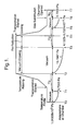
- Fig. 1 is a chart showing an example of temperature atmosphere and pressure profiles in a chamber and a processing operation in the method according to the invention.
- an insulator substrate 2 is laminated on to a metal base 1, with a bonding solder sheet 3 placed between them.
- a silicon chip 4 is further laminated to this structure, with a bonding solder sheet 5 placed between the silicon chip and the insulator substrate.
- Such a laminate 10 is, as shown in Fig. 3, mounted on a transport stage 12 in a reduced pressure furnace 11.
- the transport stage 12 has a structure which can move back and forth between a hot plate 13 which heats the laminate 10, and a water cooling plate 14 for cooling the laminate 10.
- the reduced pressure furnace 11 is first sealed to start depressurization in the furnace (Fig. 1, timing T0).
- the transport stage 12 is in a "stand-by" state, that is, it is separated from both the hot plate 13 and the water cooling plate 14.
- hydrogen gas is introduced into the reduced pressure furnace 11 (Fig. 1, timing T1).
- the flow rate of the hydrogen gas is, for example, 10 litres per second.
- the transport stage 12 is transferred to the hot plate 13. This heats the laminate 10 until the temperature reaches a target bonding temperature.
- depressurization inside the reduced pressure furnace 11 is started again (Fig. 1, timing T2). Then, after the reduced pressure furnace 11 has been evacuated to a certain degree, for example 13.1967Pa, depressurization is continued further, for one minute, for example. This reduces the pressure in the reduced pressure furnace 11 to approximately 4.1323 to 3.7324 x 10 -1 Pa.
- the one minute continuation of the depressurization removes voids produced by insufficient wetting between the solder and the component to be bonded, along with voids produced by dissolved gas included in the solder material.
- the reason for taking the continuation time as one minute is that no further void removing effect can be obtained, even if the depressurization is continued for longer than one minute.
- the void 21 in the solder sheet 3 or 5 is filled with gases of oxidizing components.
- a portion of the solder which comes into contact with the void 21 is therefore oxidized when the void 21 passes through it. This causes the wettability of the solder in the portion which the void 21 has passed through to decrease, and a tunnel-like void is left in the solder.
- Hydrogen gas filling the open void reduces the oxidized inner surface, which helps maintain the wettability of the solder surface.
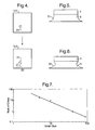
- Another reason for continuing to introduce hydrogen gas is to reduce the surface tension of the solder sheet 5, by continuing the reduction by hydrogen whilst heating the solder with the hot plate 13, thereby stabilizing a solder fillet shape 31 as shown in Fig. 5. This lengthens the solder life and decreases crack generation. As shown in Fig.6, if solidification of the solder sheet 5 by cooling is started soon after depressurization of the inside of the furnace without continuing to introduce hydrogen gas, a non-uniform solder fillet shape 32 results. This is due to the large surface tension of the solder sheet, and causes the solder life to be shortened due to the generation of cracks caused by thermal influences.
- the surface tension of the solder sheet 5 can be reduced by continuing to heat the solder sheet 5, increasing the time for exposing the solder sheet 5 to hydrogen gas, or combining them.
- the time for which the introduction of hydrogen gas is continued is adequately taken as one minute.
- the transport stage 12 is transferred from the hot plate 13 to the water cooling plate 14, which begins to cool the laminate 10 down (Fig. 1, timing T4).
- the laminate 10 is cooled at a rate of, for example, 300°C per minute.
- the temperature of the laminate 10 becomes, for example, 50 to 60°C, removal of the hydrogen gas in the reduced pressure furnace 11 begins (Fig. 1, timing T5).
- the temperature of the hot plate 13 is preferably higher than the melting point of solder (by around 50°C).
- the temperature of the hot plate 13 is taken as 350 to 360°C, with variations within the surface thereof taken into consideration.
- the temperature of the hot plate 13 is 280 to 290°C according to the above explanation.
- the temperature of the hot plate 13 is preferably taken as 300 to 310°C.
- the rate of cooling (rate of solidification) of the solder must be taken into consideration. More specifically, in the processes described above, the silicon chip 4, the insulator substrate 2, and the metal base 1, which differ in their coefficients of thermal expansion, are simultaneously solder bonded. Once soldering is completed, this causes the metal base 1, which has the largest coefficient of thermal expansion, to warp out of shape so as to become convex toward the side of the insulator substrate 2. This influences the entire laminate 10 through the solder-bonded layers, to cause a maximum warping in the order of 0.3mm. If this deformation is present during the next wire bonding step, it can cause a failure in electrical characteristics as explained above. Therefore, it is necessary to remove the deformation before carrying out the wire bonding step.
- Fig. 7 is a characteristic diagram showing a relationship between a grain size and a rate of creep of Sn-Pb solder (Sn-37Pb solder). It is known from the diagram that the rate of creep tends to increase as the diameter of the grain decreases. The tendency is the same in a solder material with a different ratio of composition of Sn and Pb. Therefore, by increasing the rate of creep, the metal structure (grain) can be made more fine.
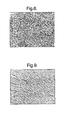
- Figs. 8 and 11 show SEM images of metal structures of Sn-Pb solder (Sn-37Pb solder) when the cooling rate is changed.
- Figs. 8 to 11 are images for the cooling rates of 600°C per minute, 300°C per minute, 5°C per minute, and 0.5°C per minute, respectively. From these images, it can be seen that the solder structure becomes finer as the cooling rate increases. Therefore, from the relationships of rate of creep to grain size to cooling rate, it is known that the rate of creep can be increased by increasing the cooling rate (rate of solidification) of the solder. Therefore, the cooling rate is preferably taken as 250°C per minute or more, for example, as 300°C per minute.
- the cooling rate of 250°C per minute or more causes the deformation of the metal base 1 to fall to within a range of 0 to -0.1mm (the sign "-" indicates that the warp is convex toward the side of the insulator substrate 2), which can eliminate an adverse effect on wire bonding.
- the cooling rate of 250°C per minute or less cannot sufficiently restore the warped metal base 1 so that the wire bonding is liable to be adversely affected.
- the temperature and cooling time of the water cooling plate 14 are selected so that the cooling rate of the solder is 250°C per minute or more.
- the size of the solder sheet 5 is also 5mm square or less.
- Such considerably small sizes of the silicon chip and the solder sheet cause preliminary preparation of soldering to be time consuming, or cause insufficient positioning of the silicon chip 4 to the solder sheet 5, which can produce bonding failure.
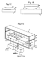
- Fig. 14 is a cross sectional view showing an example of an arrangement inside a reduced pressure furnace.
- the reduced pressure furnace 11 includes a main body 111 and a lid 113 put thereon, with packing 112 held between them in order to keep the inside of the furnace gas tight.
- a hydrogen gas introducing pipe 114 for supplying hydrogen gas to the furnace
- a nitrogen gas introducing pipe 115 for supplying nitrogen gas to the furnace
- an exhaust hole 116 there are provided in the reduced pressure furnace 11.
- the hydrogen gas introducing pipe 114 is attached onto the rear side of the hot plate 13 in a spiral, spreading from the centre thereof toward outside. This is not shown in Fig. 14, however, in order to avoid complication of the figure.
- An arrangement is provided in which, from a plurality of holes provided on the spiral pipe, hydrogen gas heated by the hot plate 13 is uniformly blown off into the inside of the furnace. This enhances the reducing power.
- the hydrogen gas introducing pipe 114 and the nitrogen gas introducing pipe 115 are connected to a hydrogen gas supply source and a nitrogen gas supply source (not shown) respectively, outside the furnace.
- a vacuum pump 15 is connected to the exhaust hole 116.
- the water cooling plate 14 is connected to a chiller 16 on the outside of the furnace for circulating cooling water for the water cooling plate 14. Moreover, the transport stage 12 travels along transporting rails 17 between the hot plate 13 and the water cooling plate 14.
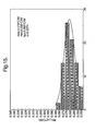
- Fig. 15 shows an example of the thermal resistance distribution in a plurality of semiconductor devices manufactured by a method according to the invention.
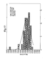
- Fig. 17 shows an example of the thermal resistance distribution in a plurality of semiconductor devices manufactured by the first method of the above-explained prior art.
- an averaged value, the maximum value, and the minimum value of the thermal resistance distribution are 0.266°C/W, 0.279°C/W, and 0.250°C/W, respectively.
- the standard deviation is 0.0074.
- the averaged value, the maximum value, the minimum value, and the standard deviation of the thermal resistance distribution are 0.287°C/W, 0.334°C/W, and 0.272°C/W, and 0.0103, respectively.
- values of the thermal resistance and the deviation thereof are apparently smaller in the method according to the present invention. Namely, it was ascertained that a void fraction in a solder bonded layer and the deviation thereof can be made smaller by the method according to the invention than those in the conventional method, thereby enhancing the heat dissipation of the semiconductor device.
- the solder sheet 3, the insulator substrate 2, the solder sheet 5, and the silicon chip 4 are laminated, in that order, on the metal base 1.
- the laminate 10 is fed into the bonding assembling apparatus provided with a reduced pressure furnace 11. After evacuating the inside of the furnace, a surface of each of the components included in the laminate 10 is reduced by introducing hydrogen into the furnace 11 until the pressure inside the furnace 11 is greater than atmospheric pressure. After the solder is heated and melted, the voids in the solder sheets 3 and 5 are removed by evacuating until it contains a vacuum the furnace again.
- the invention is not limited to the method described above, but can be modified.
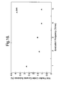
- the evacuation steps between the timings T2 and T3 in Fig. 1 are normally carried out once.
- the evacuation step can be repeated a plurality of times. Depressurization and pressurization repeated in this way cause shaking in the melting solder which eases the removal of the voids.
- Fig. 16 shows the relationship between the frequency of evacuation and the void fraction in the solder bonded layer where the evacuation is repeated up to five times. The void fraction becomes small as the frequency is increased, however after five repetitions no further affect is obtained by a further increase in frequency.
- the hot plate and the cooling plate are disposed in close proximity to each other in the reduced pressure furnace. Therefore, the temperature of the portion of the hot plate adjacent to the cooling plate decreases. Meanwhile, the temperature of the portion of the cooling plate adjacent to the hot plate increases.
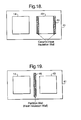
- Figs. 18 to 21 Examples of ways of eliminating these portion with such non-uniform temperature are shown in Figs. 18 to 21.
- thermal insulation is provided by ceramic walls 44 on the outer periphery of a hot plate 43 in the reduced pressure furnace, in order to prevent thermal interference.
- a partition wall 45 is provided between the hot plate 43 and the cooling plate 14 to prevent thermal interference.
- iron group materials and ceramic materials may be used to construct the partition wall 45.
- a carbon plate 46 which has a thickness of 2 to 3mm is laid on the hot plate 43.
- the carbon plate 46 which is made of a material which heats up easily but is difficult to cool, retains the heat so as to maintain the uniform temperature of the hot plate, and therefore no heat can be transferred to the cooling plate14.
- a heat shield plate 47 is provided above the hot plate 43, thereby keeping active hydrogen near the hot plate 43. This causes the arrangement to exhibit a hydrogen activation effect at soldering, and results in heat insulation by hydrogen gas around the hot plate 43.
- solder bonding of a metal base and an insulator substrate and solder bonding of the insulator substrate and a silicon chip are simultaneously performed. Meanwhile, voids in the solder are removed and warping of the metal base caused by the bonding of different kinds of materials is quickly removed. Therefore, within ten minutes from beginning the operation of a reduced pressure furnace, a semiconductor device can be obtained which has solder bonded layers of higher quality and reliability and which dissipates heat more efficiently than conventional ones. Additionally, operational costs are reduced and adverse effects on the environment are prevented by the method according to the invention.
Landscapes
- Engineering & Computer Science (AREA)
- Mechanical Engineering (AREA)
- Die Bonding (AREA)
Abstract
Description
Claims (12)
- A method of manufacturing a semiconductor device comprising the steps of:feeding a laminate (10) into a reduced pressure furnace (11), the laminate including at least two components (1, 2, 4) to be bonded with a solder sheet (3, 5) there between;evacuating the inside of the reduced pressure furnace in a first depressurization step;introducing hydrogen into the reduced pressure furnace in a first reduction step, until the pressure in the reduced pressure furnace is higher than atmospheric pressure, before heating and melting the solder sheet; andduring the first reduction step, heating the inside of the reduced pressure furnace to a bonding temperature to melt the solder sheet while maintaining the composition and pressure of the atmosphere therein.
- The method according to claim 1 further comprising the step of, after heating the reduced pressure furnace (11), removing the voids (21) in the liquefied solder by evacuating the reduced pressure furnace, while keeping the temperature therein at the bonding temperature.
- A method of manufacturing a semiconductor device comprising the steps of the method of claim 1, further including the steps of:removing the voids (21) in the liquefied solder by evacuating the reduced pressure furnace (11), while keeping the temperature therein at the bonding temperature; andintroducing hydrogen into the reduced pressure furnace in a second reduction step, until the pressure in the reduced pressure furnace is higher than atmospheric pressure while keeping the temperature therein at the bonding temperature, and maintaining this for a specified length of time.
- A method of manufacturing a semiconductor device including the steps of:feeding a laminate (10) into a reduced pressure furnace (11), the laminate including at least two components (1, 2, 4) to be bonded with a solder sheet (3, 5) there between;heating the laminate up to a bonding temperature to melt the solder sheet;removing the voids (21) in the liquefied solder by evacuating the reduced pressure furnace, while keeping the temperature therein at the bonding temperature; andintroducing hydrogen into the reduced pressure furnace in a second reduction step, until the pressure in the reduced pressure furnace is higher than atmospheric pressure while keeping the temperature therein at the bonding temperature, and maintaining this for a specified length of time.
- The method according to claims 3 or 4, further comprising the step of rapidly cooling the laminate (10) while maintaining the composition and pressure of the atmosphere inside the reduced pressure furnace (11).
- The method according to claim 5, further comprising the steps of:making the solder structure finer to increase the rate of creep during cooling in order to remove warping of the components (1, 2, 4) to be bonded due to differences in coefficients of thermal expansion among the components;during the cooling step, evacuating the reduced pressure furnace (11) in a second depressurization step; andafter the second depressurization step, introducing nitrogen into the reduced pressure furnace until the pressure in the reduced pressure furnace is higher than atmospheric pressure, before opening the reduced pressure furnace.
- The method according to either of claims 5 or 6, wherein the rate of cooling is 250°C per minute or more, and preferably 300°C per minute or more.
- The method according to any of claims 5 to 7 wherein, during cooling, the atmosphere of hydrogen inside the reduced pressure furnace (11) is replaced by the atmosphere of nitrogen when the temperature therein becomes 60°C or below.
- The method according to any of claims 2 to 8 wherein, during void removing step, the steps of introducing hydrogen into the reduced pressure furnace (11) until the pressure in the reduced pressure furnace is higher than atmospheric pressure, and removing the voids (21) in the liquefied solder by evacuating the reduced pressure furnace while keeping the temperature therein at the bonding temperature, may be carried out between one and five times.
- The method according to any preceding claim, wherein the hydrogen gas, while being heated by a heating plate (13, 43) heating the laminate (10) on the inside of the reduced pressure furnace(11), is uniformly supplied over the heating plate.
- The method according to any preceding claim wherein, while the solder sheet (3, 5) is melting, the oxygen concentration inside the reduced pressure furnace (11) is kept at 30ppm or below, and wherein the dew point thereof is kept at -30°C or below.
- The method according to any of claims 1 to 15, wherein the oxygen concentration inside the reduced pressure furnace (11) is kept at 10ppm or below, and wherein the dew point thereof is kept at -50°C or below.
Applications Claiming Priority (2)
| Application Number | Priority Date | Filing Date | Title |
|---|---|---|---|
| JP2002094650 | 2002-03-29 | ||
| JP2002094650A JP3809806B2 (en) | 2002-03-29 | 2002-03-29 | Manufacturing method of semiconductor device |
Publications (3)
| Publication Number | Publication Date |
|---|---|
| EP1350588A2 true EP1350588A2 (en) | 2003-10-08 |
| EP1350588A3 EP1350588A3 (en) | 2004-09-22 |
| EP1350588B1 EP1350588B1 (en) | 2006-08-02 |
Family
ID=28035863
Family Applications (1)
| Application Number | Title | Priority Date | Filing Date |
|---|---|---|---|
| EP03251732A Expired - Lifetime EP1350588B1 (en) | 2002-03-29 | 2003-03-20 | Method of manufacturing semiconductor device |
Country Status (5)
| Country | Link |
|---|---|
| US (1) | US6905063B2 (en) |
| EP (1) | EP1350588B1 (en) |
| JP (1) | JP3809806B2 (en) |
| CN (1) | CN1266753C (en) |
| DE (1) | DE60307157T2 (en) |
Cited By (4)
| Publication number | Priority date | Publication date | Assignee | Title |
|---|---|---|---|---|
| DE102007010882A1 (en) * | 2007-03-06 | 2008-09-25 | Infineon Technologies Ag | Solder connection for use between semiconductor chip and substrate, has soldering material layer arranged between power semiconductor chip and upper surface region of substrate, where layer exhibits repeatedly meltable soldering material |
| WO2013057252A3 (en) * | 2011-10-21 | 2013-08-29 | Asscon Systemtechnik-Elektronik Gmbh | Device and method for soldering |
| CN110402076A (en) * | 2018-04-25 | 2019-11-01 | 松下知识产权经营株式会社 | Component mounting line, component mounting method and quality control system |
| EP3706161A4 (en) * | 2017-10-31 | 2021-03-10 | Senju Metal Industry Co., Ltd | BRAZED SEAL AND BRAZED SEAL FORMING PROCESS |
Families Citing this family (39)
| Publication number | Priority date | Publication date | Assignee | Title |
|---|---|---|---|---|
| US7306133B2 (en) * | 2003-04-25 | 2007-12-11 | St Assembly Test Services Ltd. | System for fabricating an integrated circuit package on a printed circuit board |
| JP2005205418A (en) * | 2004-01-20 | 2005-08-04 | Denso Corp | Manufacturing method of bonded structure |
| US7347354B2 (en) * | 2004-03-23 | 2008-03-25 | Intel Corporation | Metallic solder thermal interface material layer and application of the same |
| JP2007000915A (en) * | 2005-06-27 | 2007-01-11 | Shinko Seiki Co Ltd | Soldering method and soldering apparatus |
| JP2007180447A (en) * | 2005-12-28 | 2007-07-12 | Toyota Industries Corp | Soldering method, soldering apparatus, and semiconductor device manufacturing method |
| JP2007207899A (en) * | 2006-01-31 | 2007-08-16 | Toyota Industries Corp | Soldering apparatus, soldering method, and semiconductor device manufacturing method |
| JP4924920B2 (en) * | 2006-06-28 | 2012-04-25 | 三菱マテリアル株式会社 | Method for bonding the entire bonding surface of an element to a substrate using an Au-Sn alloy solder paste |
| DE102007005345B4 (en) * | 2007-02-02 | 2014-06-18 | Seho Systemtechnik Gmbh | Method for reflow soldering and device for carrying out the method |
| KR20090005488A (en) * | 2007-07-09 | 2009-01-14 | 삼성전자주식회사 | Reflow apparatus and method |
| KR20100048615A (en) * | 2008-10-31 | 2010-05-11 | 엘지디스플레이 주식회사 | Apparatus for fabricating display device |
| JP5343566B2 (en) * | 2009-01-08 | 2013-11-13 | 富士通株式会社 | Joining method and reflow apparatus |
| JP5424201B2 (en) * | 2009-08-27 | 2014-02-26 | アユミ工業株式会社 | Heat-melt treatment apparatus and heat-melt treatment method |
| JP2012074636A (en) * | 2010-09-29 | 2012-04-12 | Sumitomo Bakelite Co Ltd | Joining method, semiconductor device, multilayer circuit board, and electronic component |
| TW201301413A (en) * | 2011-06-20 | 2013-01-01 | 華新麗華股份有限公司 | Wafer bonding equipment |
| TW201301412A (en) * | 2011-06-20 | 2013-01-01 | 華新麗華股份有限公司 | Wafer bonding method |
| DE102012104707A1 (en) * | 2012-05-31 | 2013-12-05 | Benteler Automobiltechnik Gmbh | Method for producing an exhaust gas heat exchanger |
| JP6116165B2 (en) * | 2012-09-14 | 2017-04-19 | 昭和電工株式会社 | Aluminum brazing method |
| JP6144495B2 (en) * | 2013-01-24 | 2017-06-07 | オリジン電気株式会社 | Heat bonding apparatus and method for manufacturing heat bonded product |
| JP5902107B2 (en) * | 2013-01-24 | 2016-04-13 | オリジン電気株式会社 | Heat bonding apparatus and method for manufacturing heat bonded product |
| JP2014157858A (en) * | 2013-02-14 | 2014-08-28 | Fuji Electric Co Ltd | Semiconductor device manufacturing method |
| DE112014002345B4 (en) * | 2013-05-10 | 2021-02-11 | Fuji Electric Co., Ltd. | Semiconductor device and manufacturing method for the semiconductor device |
| JP2015009262A (en) * | 2013-07-01 | 2015-01-19 | 三菱電機株式会社 | Reflow device |
| JP6278251B2 (en) * | 2013-09-27 | 2018-02-14 | 富士電機株式会社 | Bonding assembly equipment |
| JP6365919B2 (en) * | 2013-09-27 | 2018-08-01 | 富士電機株式会社 | Manufacturing method of semiconductor device |
| EP3088116B1 (en) * | 2013-12-25 | 2018-06-27 | Senju Metal Industry Co., Ltd. | Vacuum soldering apparatus and control method therefor |
| JP6554788B2 (en) * | 2014-12-03 | 2019-08-07 | 富士電機株式会社 | Manufacturing method of semiconductor device |
| CN105234569A (en) * | 2015-10-13 | 2016-01-13 | 甘肃虹光电子有限责任公司 | Hydrogen furnace welding method |
| CN105428266B (en) * | 2015-11-30 | 2018-02-16 | 中国电子科技集团公司第三十八研究所 | The product of flip-chip eutectic bonding method and acquisition with medium bridge |
| CN105562868B (en) * | 2016-01-15 | 2018-11-23 | 山东融创电子科技有限公司 | A kind of semiconductor material welding technique for diode fabrication process |
| CN106229306B (en) * | 2016-07-18 | 2019-07-05 | 浙江益中智能电气有限公司 | A kind of core method in the stabilisation of power device chip |
| KR101827170B1 (en) * | 2016-11-25 | 2018-02-07 | 현대자동차주식회사 | Clip for fixing outer parts of vehicle |
| CN106601625A (en) * | 2016-12-21 | 2017-04-26 | 贵州振华风光半导体有限公司 | Clean-free hybrid integrated circuit welding method |
| CN111805039B (en) * | 2019-04-11 | 2022-02-08 | 中科同帜半导体(江苏)有限公司 | Online positive pressure welding furnace system and operation method thereof |
| DE102019218157A1 (en) * | 2019-11-25 | 2021-05-27 | Zf Friedrichshafen Ag | Power module with housed power semiconductors for the controllable electrical power supply of a consumer and a method for production |
| US12284749B2 (en) | 2019-11-25 | 2025-04-22 | Zf Friedrichshafen Ag | Power module with housed power semiconductors for controllable electrical power supply of a consumer, and method for producing same |
| CN112908954A (en) * | 2021-03-01 | 2021-06-04 | 宁波施捷电子有限公司 | Hot-pressed part and preparation method and application thereof |
| CN113385763B (en) * | 2021-07-14 | 2022-08-26 | 成都共益缘真空设备有限公司 | Vacuum reflow soldering positive and negative pressure combined soldering process |
| CN117086429A (en) * | 2023-10-18 | 2023-11-21 | 苏州申翰智能机器人有限公司 | Reflow soldering device based on semiconductor substrate and operation process thereof |
| CN117798567B (en) * | 2024-02-29 | 2024-06-04 | 西北电子装备技术研究所(中国电子科技集团公司第二研究所) | Eutectic welding table capable of rapidly increasing and decreasing temperature |
Family Cites Families (12)
| Publication number | Priority date | Publication date | Assignee | Title |
|---|---|---|---|---|
| US4448853A (en) * | 1981-04-15 | 1984-05-15 | Bbc Brown, Boveri & Company, Limited | Layered active brazing material and method for producing it |
| US4645116A (en) * | 1982-10-08 | 1987-02-24 | At&T Bell Laboratories | Fluxless bonding of microelectronic chips |
| US4614837A (en) * | 1985-04-03 | 1986-09-30 | Allied Corporation | Method for placing electrically conductive paths on a substrate |
| US4709849A (en) * | 1985-11-27 | 1987-12-01 | Fry Metals, Inc. | Solder preform and methods employing the same |
| US4860942A (en) * | 1987-11-30 | 1989-08-29 | Ceradyne, Inc. | Method for soldering void-free joints |
| JPH0779071A (en) | 1993-09-07 | 1995-03-20 | Mitsubishi Electric Corp | Electronic component soldering method and soldering apparatus |
| US6090701A (en) * | 1994-06-21 | 2000-07-18 | Kabushiki Kaisha Toshiba | Method for production of semiconductor device |
| JP3136390B2 (en) * | 1994-12-16 | 2001-02-19 | 株式会社日立製作所 | Solder joining method and power semiconductor device |
| JP3294460B2 (en) | 1995-03-06 | 2002-06-24 | 株式会社日立製作所 | Circuit board manufacturing method |
| US7124753B2 (en) * | 1997-04-04 | 2006-10-24 | Chien-Min Sung | Brazed diamond tools and methods for making the same |
| JP3753524B2 (en) | 1997-11-20 | 2006-03-08 | 株式会社日立製作所 | Manufacturing method of electronic parts |
| JP3347279B2 (en) | 1997-12-19 | 2002-11-20 | 三菱電機株式会社 | Semiconductor device and method of manufacturing the same |
-
2002
- 2002-03-29 JP JP2002094650A patent/JP3809806B2/en not_active Expired - Lifetime
-
2003
- 2003-03-20 EP EP03251732A patent/EP1350588B1/en not_active Expired - Lifetime
- 2003-03-20 CN CNB031076343A patent/CN1266753C/en not_active Expired - Lifetime
- 2003-03-20 DE DE60307157T patent/DE60307157T2/en not_active Expired - Lifetime
- 2003-03-26 US US10/400,188 patent/US6905063B2/en not_active Expired - Lifetime
Cited By (6)
| Publication number | Priority date | Publication date | Assignee | Title |
|---|---|---|---|---|
| DE102007010882A1 (en) * | 2007-03-06 | 2008-09-25 | Infineon Technologies Ag | Solder connection for use between semiconductor chip and substrate, has soldering material layer arranged between power semiconductor chip and upper surface region of substrate, where layer exhibits repeatedly meltable soldering material |
| DE102007010882B4 (en) * | 2007-03-06 | 2009-01-29 | Infineon Technologies Ag | Method for producing a solder joint between a semiconductor chip and a substrate |
| WO2013057252A3 (en) * | 2011-10-21 | 2013-08-29 | Asscon Systemtechnik-Elektronik Gmbh | Device and method for soldering |
| EP3706161A4 (en) * | 2017-10-31 | 2021-03-10 | Senju Metal Industry Co., Ltd | BRAZED SEAL AND BRAZED SEAL FORMING PROCESS |
| US10968932B2 (en) | 2017-10-31 | 2021-04-06 | Senju Metal Industry Co., Ltd. | Soldered joint and method for forming soldered joint |
| CN110402076A (en) * | 2018-04-25 | 2019-11-01 | 松下知识产权经营株式会社 | Component mounting line, component mounting method and quality control system |
Also Published As
| Publication number | Publication date |
|---|---|
| EP1350588B1 (en) | 2006-08-02 |
| US6905063B2 (en) | 2005-06-14 |
| DE60307157T2 (en) | 2006-12-07 |
| JP3809806B2 (en) | 2006-08-16 |
| US20030222126A1 (en) | 2003-12-04 |
| DE60307157D1 (en) | 2006-09-14 |
| EP1350588A3 (en) | 2004-09-22 |
| JP2003297860A (en) | 2003-10-17 |
| CN1266753C (en) | 2006-07-26 |
| CN1449005A (en) | 2003-10-15 |
Similar Documents
| Publication | Publication Date | Title |
|---|---|---|
| EP1350588B1 (en) | Method of manufacturing semiconductor device | |
| KR101049427B1 (en) | Soldering method | |
| CN105679686B (en) | The manufacturing method and engagement assembling device of semiconductor device | |
| CN104517865A (en) | Semi-conductor device manufacture method | |
| JP3207506B2 (en) | Manufacturing method of electronic circuit device | |
| US20050156324A1 (en) | Method for manufacturing connection construction | |
| CN104517860B (en) | Engage assembling device | |
| TWI723424B (en) | Manufacturing method of semiconductor device | |
| CN103459075B (en) | Soldering apparatus, soldering method, and produced substrate and electronic component | |
| US8944310B2 (en) | Method of manufacturing a semiconductor device | |
| JPH08168876A (en) | Solder joining method and power semiconductor device | |
| JP4864591B2 (en) | Soldering method and soldering apparatus | |
| EP1295665B1 (en) | Method of manufacturing mount structure without introducing degraded bonding strength of electronic parts due to segregation of low-strength/low-melting point alloy | |
| CN115472513A (en) | Vacuum backflow process for chip welding and mounting | |
| JP2015103688A (en) | Bonding method, semiconductor device, manufacturing system and oxide film removing device (chip bonding process using non-cleaning flux) | |
| JPH04196333A (en) | Method and device for solid-phase welding | |
| JPH11121921A (en) | Electronic component soldering method and apparatus | |
| US9434028B2 (en) | Soldering method and method of manufacturing semiconductor device | |
| JP3240876B2 (en) | Mounting method of chip with bump | |
| JP2002368044A (en) | Method of assembling electronic component with solder ball and electronic component | |
| JP3385925B2 (en) | Electronic circuit manufacturing method | |
| CN121693204A (en) | Method and apparatus for forming an electronic device | |
| Barnes | Void free die attachment for multichip modules using solder alloys | |
| JPH03207573A (en) | Method and apparatus for producing joined body | |
| JPH08277172A (en) | Interface cleaning solder joining method and device and applied products |
Legal Events
| Date | Code | Title | Description |
|---|---|---|---|
| PUAI | Public reference made under article 153(3) epc to a published international application that has entered the european phase |
Free format text: ORIGINAL CODE: 0009012 |
|
| AK | Designated contracting states |
Kind code of ref document: A2 Designated state(s): AT BE BG CH CY CZ DE DK EE ES FI FR GB GR HU IE IT LI LU MC NL PT RO SE SI SK TR |
|
| AX | Request for extension of the european patent |
Extension state: AL LT LV MK |
|
| PUAL | Search report despatched |
Free format text: ORIGINAL CODE: 0009013 |
|
| AK | Designated contracting states |
Kind code of ref document: A3 Designated state(s): AT BE BG CH CY CZ DE DK EE ES FI FR GB GR HU IE IT LI LU MC NL PT RO SE SI SK TR |
|
| AX | Request for extension of the european patent |
Extension state: AL LT LV MK |
|
| 17P | Request for examination filed |
Effective date: 20040930 |
|
| 17Q | First examination report despatched |
Effective date: 20050406 |
|
| AKX | Designation fees paid |
Designated state(s): DE GB |
|
| GRAP | Despatch of communication of intention to grant a patent |
Free format text: ORIGINAL CODE: EPIDOSNIGR1 |
|
| GRAS | Grant fee paid |
Free format text: ORIGINAL CODE: EPIDOSNIGR3 |
|
| GRAA | (expected) grant |
Free format text: ORIGINAL CODE: 0009210 |
|
| AK | Designated contracting states |
Kind code of ref document: B1 Designated state(s): DE GB |
|
| REG | Reference to a national code |
Ref country code: GB Ref legal event code: FG4D |
|
| REF | Corresponds to: |
Ref document number: 60307157 Country of ref document: DE Date of ref document: 20060914 Kind code of ref document: P |
|
| PLBE | No opposition filed within time limit |
Free format text: ORIGINAL CODE: 0009261 |
|
| STAA | Information on the status of an ep patent application or granted ep patent |
Free format text: STATUS: NO OPPOSITION FILED WITHIN TIME LIMIT |
|
| 26N | No opposition filed |
Effective date: 20070503 |
|
| PGFP | Annual fee paid to national office [announced via postgrant information from national office to epo] |
Ref country code: GB Payment date: 20080326 Year of fee payment: 6 |
|
| GBPC | Gb: european patent ceased through non-payment of renewal fee |
Effective date: 20090320 |
|
| PG25 | Lapsed in a contracting state [announced via postgrant information from national office to epo] |
Ref country code: GB Free format text: LAPSE BECAUSE OF NON-PAYMENT OF DUE FEES Effective date: 20090320 |
|
| REG | Reference to a national code |
Ref country code: DE Ref legal event code: R082 Ref document number: 60307157 Country of ref document: DE Representative=s name: GRUENECKER, KINKELDEY, STOCKMAIR & SCHWANHAEUS, DE Effective date: 20110826 Ref country code: DE Ref legal event code: R081 Ref document number: 60307157 Country of ref document: DE Owner name: FUJI ELECTRIC CO., LTD., JP Free format text: FORMER OWNER: FUJI ELECTRIC SYSTEMS CO., LTD., TOKYO/TOKIO, JP Effective date: 20110826 Ref country code: DE Ref legal event code: R081 Ref document number: 60307157 Country of ref document: DE Owner name: FUJI ELECTRIC CO., LTD., KAWASAKI-SHI, JP Free format text: FORMER OWNER: FUJI ELECTRIC SYSTEMS CO., LTD., TOKYO/TOKIO, JP Effective date: 20110826 Ref country code: DE Ref legal event code: R082 Ref document number: 60307157 Country of ref document: DE Representative=s name: GRUENECKER PATENT- UND RECHTSANWAELTE PARTG MB, DE Effective date: 20110826 |
|
| PGFP | Annual fee paid to national office [announced via postgrant information from national office to epo] |
Ref country code: DE Payment date: 20220203 Year of fee payment: 20 |
|
| REG | Reference to a national code |
Ref country code: DE Ref legal event code: R071 Ref document number: 60307157 Country of ref document: DE |