EP1382411A2 - Procédé de mesure du profil d'intensité d'un faisceau d'électrons,notamment d'un faisceau d'un dispositif d'usinage par faisceau d'électrons,et/ou de mesure d'une optique pour un faisceau d'électrons et/ou d'ajustage d'une optique pour un faisceau d'électrons,structure de mesure pour un tel procédé et dispositif d'usinage par faisceau d'électrons - Google Patents
Procédé de mesure du profil d'intensité d'un faisceau d'électrons,notamment d'un faisceau d'un dispositif d'usinage par faisceau d'électrons,et/ou de mesure d'une optique pour un faisceau d'électrons et/ou d'ajustage d'une optique pour un faisceau d'électrons,structure de mesure pour un tel procédé et dispositif d'usinage par faisceau d'électrons Download PDFInfo
- Publication number
- EP1382411A2 EP1382411A2 EP03015282A EP03015282A EP1382411A2 EP 1382411 A2 EP1382411 A2 EP 1382411A2 EP 03015282 A EP03015282 A EP 03015282A EP 03015282 A EP03015282 A EP 03015282A EP 1382411 A2 EP1382411 A2 EP 1382411A2
- Authority
- EP
- European Patent Office
- Prior art keywords
- electron beam
- measuring structure
- measuring
- backscatter
- optics
- Prior art date
- Legal status (The legal status is an assumption and is not a legal conclusion. Google has not performed a legal analysis and makes no representation as to the accuracy of the status listed.)
- Granted
Links
Images



Classifications
-
- H—ELECTRICITY
- H01—ELECTRIC ELEMENTS
- H01J—ELECTRIC DISCHARGE TUBES OR DISCHARGE LAMPS
- H01J37/00—Discharge tubes with provision for introducing objects or material to be exposed to the discharge, e.g. for the purpose of examination or processing thereof
- H01J37/30—Electron-beam or ion-beam tubes for localised treatment of objects
- H01J37/315—Electron-beam or ion-beam tubes for localised treatment of objects for welding
-
- B—PERFORMING OPERATIONS; TRANSPORTING
- B23—MACHINE TOOLS; METAL-WORKING NOT OTHERWISE PROVIDED FOR
- B23K—SOLDERING OR UNSOLDERING; WELDING; CLADDING OR PLATING BY SOLDERING OR WELDING; CUTTING BY APPLYING HEAT LOCALLY, e.g. FLAME CUTTING; WORKING BY LASER BEAM
- B23K15/00—Electron-beam welding or cutting
-
- H—ELECTRICITY
- H01—ELECTRIC ELEMENTS
- H01J—ELECTRIC DISCHARGE TUBES OR DISCHARGE LAMPS
- H01J37/00—Discharge tubes with provision for introducing objects or material to be exposed to the discharge, e.g. for the purpose of examination or processing thereof
- H01J37/30—Electron-beam or ion-beam tubes for localised treatment of objects
- H01J37/304—Controlling tubes by information coming from the objects or from the beam, e.g. correction signals
-
- H—ELECTRICITY
- H01—ELECTRIC ELEMENTS
- H01J—ELECTRIC DISCHARGE TUBES OR DISCHARGE LAMPS
- H01J2237/00—Discharge tubes exposing object to beam, e.g. for analysis treatment, etching, imaging
- H01J2237/30—Electron or ion beam tubes for processing objects
- H01J2237/304—Controlling tubes
- H01J2237/30433—System calibration
-
- H—ELECTRICITY
- H01—ELECTRIC ELEMENTS
- H01J—ELECTRIC DISCHARGE TUBES OR DISCHARGE LAMPS
- H01J2237/00—Discharge tubes exposing object to beam, e.g. for analysis treatment, etching, imaging
- H01J2237/30—Electron or ion beam tubes for processing objects
- H01J2237/304—Controlling tubes
- H01J2237/30455—Correction during exposure
-
- H—ELECTRICITY
- H01—ELECTRIC ELEMENTS
- H01J—ELECTRIC DISCHARGE TUBES OR DISCHARGE LAMPS
- H01J2237/00—Discharge tubes exposing object to beam, e.g. for analysis treatment, etching, imaging
- H01J2237/30—Electron or ion beam tubes for processing objects
- H01J2237/304—Controlling tubes
- H01J2237/30472—Controlling the beam
- H01J2237/30477—Beam diameter
Definitions
- the invention relates to a method for measuring the Intensity profile of an electron beam, in particular a beam of an electron beam processing apparatus, and / or for measuring an optic for an electron beam and / or for adjusting an optic for an electron beam, a measuring structure for such a method and an electron beam processing device.
- optics for an electron beam any Arrangement are understood, which the geometry the beam cross section of an electron beam and / or the orientation of the beam axis of an electron beam can influence.
- These are in practice electrical and / or magnetic optical components, in particular electric and / or magnetic lenses, stigmators and Deflector.
- An optic can be through a single such component be formed or meherer include such components.
- Electron beam welder used electron beam knows and measures as soon as possible before the process can.
- mapping properties of a Beam optics of the electron beam processing apparatus and the Possibility of beam cross-section and imaging properties automatically adjust to setpoints would be for the Machining workpieces with electron beam welding advantageous.
- the measurement of the intensity profile takes place of an electron beam so that successively known Parts of the electron beam in a catcher, in particular a Faraday cage is passed.
- a catcher in particular a Faraday cage
- different measuring bodies can be used, to pass a part of the jet into the receiver, wherein the electron beam by means of a magnetic field is deflected relative to the measuring body, so that successively different cross-sectional parts of the electron beam get into the catcher.
- the simplest such measuring body comprises a threshold edge.
- Two opposite such measuring body form a Measuring structure with a slit behind which the penetrated part of the beam by a lying there Sensor is measured.
- the beam profile can be measured in one direction.
- the intensity profile of a Electron beam also in a second direction be measured, wherein the electron beam sub-beam for sub-beam is passed over the hole one after the other, by means of the o. g. Magnetic field, the control technology from Scanning Electron Microscopy is known.
- a disadvantage in the prior art is that one on the axis of the electron gun (below short: jet main axis) arranged catcher at the Place in an electron beam processing device place takes away where the workpiece is placed. A branch off from the actual electron beam path in a second Beam path arranged catcher (sensor) needs additional space. Also one has in this case for the Measurement of the intensity profiles are not exactly the same Ratio as in later welding.
- the electron beam is passed through a Relative movement to a measuring structure on different Spots of this lead the different backscatter properties and the electron current of the Backscattered electrons become dependent on the relative movement measured by electron beam and measuring structure.
- a corresponding sensor for example a sensor ring, around the electron beam around near anyway existing deflection magnets are arranged without additional space is needed.
- Another advantage of the method according to the invention is that for its implementation only a passive Measuring structure is additionally required, so that the measuring room no additional electrical cables laid have to be what are used for mass production Electron-beam welders at which the workpieces be inserted and removed on pallets, would be difficult.
- the development according to claim 2 has the advantage that Measuring structures, as they are already known used can be, wherein the transmitting part of the measuring structure, so the opening, not backscattered and the Remains of the measuring structure at least weak backscattered.
- the development according to claim 7 serves one Improvement of the backscatter behavior of the backscatter surface.
- the development of the invention according to claim 9 is in With regard to high resolution of the measuring method of advantage.
- the backscattered electrons measured in a very simple way.
- Corresponding sensor rings are also in such electron beam processing equipment often already available, where also the possibility for the raster electronic imaging of a workpiece surface consists.
- the Intensity profile within a given total deflection range for the electron beam at different uniformly distributed over the deflection area Measure digits.
- measuring structure with narrow backscattering bands, so you can easily Give a rough information of the intensity distribution in the electron beam over a larger measuring area receive.
- Such measuring structures are also suitable for debugging the imaging properties of electron beam optics and as an actual signal generator for a control circuit, with which the cross section of the electron beam is automatically minimized and / or desired imaging properties the optics are set.
- the intensity profile of the electron beam in two mutually perpendicular Measured directions so that you get a complete planar information about the energy density in the electron beam Has. Do you do this for different Focusing conditions (changing the energization of the focusing lens) or different position of the measuring structure on the beam axis, so you get a complete spatial Beam tomography.
- the method according to claim 19 allows, under Use of a regular measuring structure, which in itself for the measurement of the intensity profile of an electron beam was thought, at the same time also the imaging properties to measure the electron beam optics.
- the measuring structure specified in claim 22 has a mechanically particularly simple construction.
- the development of the measuring structure according to claim 23 serves again to falsifications of the measurement result by avoiding geometric effects.
- a measuring structure according to claim 24 is characterized mechanically very simple construction and good contrast out.
- a measuring structure as indicated in claim 28 is, on the one hand, in a simple way, the imaging properties the electron beam optics test (on the Grid lines) and at the same time the intensity profiles of the electron beam for different deflection angles easy to determine (on the backscatter surfaces).
- the claim 29 relates to a Meßvefahren, with which from the stream of passing through the measuring structure Electrons the beam cross section and / or the imaging properties the optics are determined.
- Claims 30 to 33 relate to electron beam processing equipment, where in a simple way the intensity profile of the electron beam and the imaging properties the optics for the electron beam measured can be.
- the sensors are used to measure the backscattered electrons so used that a grid electronic recording made of a measuring structure, the parts with different Has back scattering properties, and this recording is then evaluated. Out of distortions in the picture, especially with the help of a computer on the quality of the magnetic optics of focusing unit and optics be closed back.
- Measuring structure which has a regular structure, in particular a grid or net covers, so usual from the optics known calculation method for calculating the distortion can be used.
- the grid or grid lines consist of one strongly backscattering material, especially a metal, while their underground from a not or only weak backscattering material is formed, for example Graphite.
- a measuring structure with regularly arranged locations increased permeability (eg holes) or with regularly arranged places increased backscatter (e.g., backscattered areas) or with a grid or mesh are the subject of the present invention, preferred Embodiments the o.g. material properties exhibit.
- a needle or more needles with ground end surface or other backscatter elements in the method for measuring the intensity profile is / are used, in a measuring structure with grid are preferably releasably used to both intensity profiles of the beam as well as imaging properties of the To be able to measure optics.
- a backscatter arrangement and a backscattering grid arrangement also on laterally adjacent Areas of the top of the base of a measuring structure provide so that these areas optionally on the main beam axis can be made.
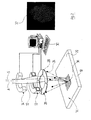
- an electron beam welder becomes an electron beam 10 of one shown as a single lens 12 focusable focusing unit.
- This can in particular a stigmator (two at 90 ° arranged Cylindrical lenses) which are separately controllable, to modify the shape of the beam cross section, in particular to bring to circular shape.
- the main beam direction is indicated at A, this is the direction in which the electron beam 10 of not shown in detail electron gun of the welding machine is generated and in which he on a workpiece (not shown) under working conditions hits if it is not distracted.
- the electron beam 10 can by means of a magnetic Deflection unit 14, which lies behind the lens 12, vertically be deflected to the beam direction.
- the deflection unit 14 comprises at least two separately controllable coils (not shown in detail) for deflecting the electron beam 10 in two mutually perpendicular directions.
- the focusing unit 12 and the optics 14 form together an optic 15 of the electron beam welding apparatus.
- This consists of a graphite plate as the 18th trained base with a flat surface 20, of in the central area, i. in the area to which the Electron beam 10 impinges when it comes from the deflection unit 14 is not strongly deflected, vertically upwards a tungsten needle 22 protrudes.
- the tungsten needle 22 is at its to the electron beam source pointing, perpendicular to the main beam direction A standing flat end surface smoothed. Also the Surface 20 of the graphite plate 18 is perpendicular the main ray direction A.
- the diameter of the tungsten needle 22 is dimensioned so that it is significantly smaller than the diameter of the electron beam 10 is.
- the smooth ground transversal end face of the tungsten needle 22 acts strongly backscattering, i. Electrons from the Electron beam 10 are in the direction A, from which the Electron beam 10 comes in one direction with a Component in the direction of the electron source, deflected back. Backscatter electrons from the needle 22, which received when the electron beam 10 is the tip of the needle 22 sweeps are in Figure 1 schematically at 24 suggests.
- the backscattered electrons are detected by means of a sensor ring, which is generally indicated at 26 and four sensor segments 28 is measured, with the sensor ring 26th the path of the electron beam seen in cross section surrounds, wherein the sensor ring is a conventional ring the kind is, as it usually in grid electronic Observation devices for collecting backscattered electrons is used. For this reason, the Sensor ring 26 both for measuring the current of the backscattered electrons as well as for imaging.
- the mean direction of the Electron beam can be understood as used by the Optics 14 is generated, apart from deflections smaller Amplitude that occurs to the electron beam 10 over the end surface of a tungsten needle 22 to raster.
- the electron beam 10 in diameter in the Level of the measuring structure 16 and the surface 20 larger is as the tungsten needle 22, meet when painting the tungsten needle 22 by the electron beam 10 different Electron beam parts on the tungsten needle, and a different intensity of the beam in these Split leads to a different number of backscattered electrons.
- the optics 15 of a Computing, control and storage unit 30 electronically controlled, and signals from the sensor ring are the Arithmetic, control and storage unit 30 supplied and in Detected depending on the deflection control signals.
- the focusing unit 12 and the deflection unit 14 separately controllable are separately controllable.
- FIG. 34 With another measuring structure, shown in FIG is and is designated there by 34, can be using essentially the same construction Goodness of the lens 12 and the deflector 14 measure what an important piece of information for assessing the quality represents the electron beam welding device.
- the measuring structure 34 also includes a graphite plate here 18 with a surface 20.
- a Metal net 36 i. a network whose network lines are made of metal consist. The net can lie directly on the graphite 18, so that also backscattered electrons 24 from the lines of the network, while the graphite background does not backscatter.
- FIG. 1 A difference from FIG. 1 also exists insofar as 36 better network picture of lens 12 and place Deflection unit 14 are reversed.
- Image forming method can be done by means of the sensor ring 26 shows an image 38 of the metal mesh 36 in front of the graphite background be generated.
- image 38 evaluation may be due to deviations of the individual lines from theirs straight course and the distortions at the edge of the pictured Net on the quality of the magnetic optics of the deflection unit 14 be inferred.
- the measuring structure 34 may - as a modification - part of the measuring structure 16 be from Figure 1, in which case the tungsten needle 22 in a small graphite plate in the large graphite plate 18 is used, and then removed is the metal net 36 in the graphite plate 18 then Approved.
- a needle assembly and a Grid arrangement also lying side by side on a common Provide base graphite plate and the two Parts of the graphite plate alternatively in the beam path make, e.g. with a calibrated threaded spindle or with a small cylinder and the end plates prescriptive attacks.
- the measuring structures 16 and 34 and the above-mentioned combined measuring structures are designed so that they easy and precise in the electron beam welding machine can be used and easily removed again (e.g., using dowel pins), so that the electron beam welding machine its actual Exercise function. It suffices for this, if in one Image plane the ability to accurately positioned Attachment of the graphite plate 18 is.
- the measuring structures 16 and 34 are passive components, do not need additional lines in the measuring space / working space the electron beam welding device are laid, around the beam cross section and the imaging properties optics 15 to determine.
- FIG. 3 shows in plan view a measuring structure 16, which again a base 20 made of graphite.
- the upper boundary surface the base 20 is concavely curved spherical, wherein the radius of the upper end face 40 the distance of the base 20 from the main point H of the beam deflecting unit 14 of the electron beam welding apparatus equivalent.
- the main point should be understood the point at which the electron beam in idealized representation of the direction of incidence kinks (similar to optical Lenses).
- a network 42 is applied, which arranged from each other at right angles Sets of backscattering 44, 46 consists.
- the backscatter bands 44, 46 are again made of a high-density metal such as. Tungsten manufactured and can be on any be prepared known manner, e.g. by cutting out from a thin polished sheet with a laser beam or by gluing appropriately narrow polished ones Ribbons in the desired pattern on the face 40th
- FIG. 5 the cross section of FIG. 5, so that their free tops each form a backscatter surface 48.
- FIG. 6 shows a middle section through a further one modified measuring structure 16, wherein the base 20th single tungsten needles 22 carries, each obliquely are made that their axis through the main point H the electron beam deflection unit runs.
- the measuring structure 16 of Figure 6 thus has a variety of small backplanes, each perpendicular to the Direction of a deflected electron beam and have the same distance from the main point H.
- the tungsten needles 22 are either arranged so that her foot sections on the top of the base 20 a square Form grid, or even so, that respectively a set of tungsten needles 22 equidistant from the axis of the electron gun are arranged and the belonging to this sentence tungsten needles 22 in the circumferential direction arranged at equidistant angular distance are.
- the further modified measuring structure according to FIG. 7 is similar in the right part of that of Figure 6 with the proviso that the ends of the tungsten needles 22 are all in the same Lie flat and are preferably arranged there, the end faces form a square grid.
- the tungsten needles 22 all perpendicular to the surface of the base 20.
- a such arrangement of the tungsten needles 22 may sometimes occur be of interest if you are not at the intensity distribution the electrons in the electron beam itself (perpendicular to the beam direction S) is interested but only at the electron distribution, as far as for the Welding is relevant (or even if the deflection radius is big against the deflection distance).
- the workpiece surface usually perpendicular to the main beam direction A of the electron gun is, form the many backscattering end faces of the tungsten needles 22 according to the left half of Figure 7, the workpiece surface at a variety of support points.
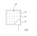
- the embodiment of Figure 8 shows a measuring arrangement for measuring beam cross-section and imaging properties, the one measuring structure 16 and a rear this lying electrically conductive collector plate 50th includes.
- the measuring structure 16 consists of a plate 52 made of tungsten, in the regular grid small diameter having drilled holes 54 are incorporated, e.g. by electron beam drilling.
- This arrangement works in transmission and measures the Electricity from the with an ammeter (not shown) connected collector plate 50 trapped electrons depending on the deflection (and possibly the focus) of the electron beam.
Landscapes
- Chemical & Material Sciences (AREA)
- Analytical Chemistry (AREA)
- Engineering & Computer Science (AREA)
- Mechanical Engineering (AREA)
- Electron Sources, Ion Sources (AREA)
- Analysing Materials By The Use Of Radiation (AREA)
Applications Claiming Priority (2)
| Application Number | Priority Date | Filing Date | Title |
|---|---|---|---|
| DE10232230 | 2002-07-17 | ||
| DE10232230A DE10232230A1 (de) | 2002-07-17 | 2002-07-17 | Verfahren zum Vermessen des Intensitätsprofils eines Elektronenstrahls, insbesondere eines Strahls eines Elektronenstrahlbearbeitungsgeräts, und/oder zum Vermessen einer Optik für einen Elektronenstrahl und/oder zum Justieren einer Optik für einen Elektronenstrahl, Meßstruktur für ein solches Verfahren und Elektronenstrahlbearbeitungsgerät |
Publications (3)
| Publication Number | Publication Date |
|---|---|
| EP1382411A2 true EP1382411A2 (fr) | 2004-01-21 |
| EP1382411A3 EP1382411A3 (fr) | 2004-02-11 |
| EP1382411B1 EP1382411B1 (fr) | 2011-10-05 |
Family
ID=29762007
Family Applications (1)
| Application Number | Title | Priority Date | Filing Date |
|---|---|---|---|
| EP03015282A Expired - Lifetime EP1382411B1 (fr) | 2002-07-17 | 2003-07-07 | Procédé de mesure du profil d'intensité d'un faisceau d'électrons,notamment d'un faisceau d'un dispositif d'usinage par faisceau d'électrons,et/ou de mesure d'une optique pour un faisceau d'électrons et/ou d'ajustage d'une optique pour un faisceau d'électrons,structure de mesure pour un tel procédé et dispositif d'usinage par faisceau d'électrons |
Country Status (3)
| Country | Link |
|---|---|
| US (1) | US6977382B2 (fr) |
| EP (1) | EP1382411B1 (fr) |
| DE (1) | DE10232230A1 (fr) |
Families Citing this family (14)
| Publication number | Priority date | Publication date | Assignee | Title |
|---|---|---|---|---|
| US20060196853A1 (en) * | 2005-03-04 | 2006-09-07 | The Regents Of The University Of California | Micro-joining using electron beams |
| US7375345B2 (en) * | 2005-10-26 | 2008-05-20 | Tetra Laval Holdings & Finance S.A. | Exposed conductor system and method for sensing an electron beam |
| DE102009050521B4 (de) * | 2009-10-23 | 2023-02-16 | Pro-Beam Ag & Co. Kgaa | Thermisches Materialbearbeitungsverfahren |
| US8791426B2 (en) * | 2009-11-24 | 2014-07-29 | Lawrence Livermore National Security, Llc. | Electron beam diagnostic system using computed tomography and an annular sensor |
| DE102012102608B4 (de) | 2012-03-27 | 2016-07-21 | Aixacct Systems Gmbh | Verfahren zur Ermittlung von Strahlparametern eines Ladungsträgerstrahls, Messeinrichtung sowie Ladungsträgerstrahlvorrichtung |
| US9383460B2 (en) * | 2012-05-14 | 2016-07-05 | Bwxt Nuclear Operations Group, Inc. | Beam imaging sensor |
| US9535100B2 (en) | 2012-05-14 | 2017-01-03 | Bwxt Nuclear Operations Group, Inc. | Beam imaging sensor and method for using same |
| US10049852B2 (en) | 2014-11-05 | 2018-08-14 | Howmedica Osteonics Corp. | Assessment and calibration of a high energy beam |
| US9324541B1 (en) * | 2014-11-18 | 2016-04-26 | Exnodes Inc. | Certified wafer inspection |
| AU2018273352B2 (en) | 2017-05-22 | 2023-07-27 | Howmedica Osteonics Corp. | Device for in-situ fabrication process monitoring and feedback control of an electron beam additive manufacturing process |
| DE102018210522B4 (de) * | 2018-06-27 | 2021-03-18 | Carl Zeiss Smt Gmbh | Verfahren und Vorrichtung zur Untersuchung eines Strahls geladener Teilchen |
| US11117195B2 (en) | 2018-07-19 | 2021-09-14 | The University Of Liverpool | System and process for in-process electron beam profile and location analyses |
| DE102021202506A1 (de) | 2021-03-15 | 2022-03-24 | Carl Zeiss Smt Gmbh | Verfahren zum Bestimmen einer Strahlform eines Elektronenstrahls |
| CN118795529B (zh) * | 2024-09-12 | 2025-03-21 | 西安赛隆增材技术股份有限公司 | 一种用于增材制造设备的电子束流检测装置及方法 |
Citations (1)
| Publication number | Priority date | Publication date | Assignee | Title |
|---|---|---|---|---|
| DE10129013A1 (de) | 2001-06-15 | 2003-01-02 | Infineon Technologies Ag | Schneller A/D-Wandler mit hoher Auflösung |
Family Cites Families (9)
| Publication number | Priority date | Publication date | Assignee | Title |
|---|---|---|---|---|
| US3409799A (en) | 1966-08-29 | 1968-11-05 | Ibm | Automatic focusing system for beam devices |
| FR2085049A5 (fr) * | 1970-03-24 | 1971-12-17 | Steigerwald Strahltech | |
| US3752962A (en) * | 1972-03-14 | 1973-08-14 | Western Data Prod Inc | Magnetic card handling system |
| JPS59114818A (ja) * | 1982-12-21 | 1984-07-03 | Toshiba Corp | 電子ビ−ムパタ−ン描画方法 |
| GB8607222D0 (en) * | 1986-03-24 | 1986-04-30 | Welding Inst | Charged particle collection |
| DE3718177A1 (de) * | 1987-05-29 | 1988-12-15 | Leybold Ag | Einrichtung fuer elektronenstrahlfokussierung, insbesondere beim elektronenstrahlschweissen |
| US5169488A (en) * | 1990-10-25 | 1992-12-08 | International Business Machines Corporation | Method of forming planarized, reusable calibration grids |
| JPH1125898A (ja) * | 1997-05-08 | 1999-01-29 | Hitachi Ltd | 電子顕微鏡の分解能評価方法および分解能評価用試料 |
| JP2002008960A (ja) * | 2000-06-19 | 2002-01-11 | Advantest Corp | ターゲットマーク部材、その製造方法および電子ビーム露光装置 |
-
2002
- 2002-07-17 DE DE10232230A patent/DE10232230A1/de not_active Ceased
-
2003
- 2003-07-07 EP EP03015282A patent/EP1382411B1/fr not_active Expired - Lifetime
- 2003-07-15 US US10/619,933 patent/US6977382B2/en not_active Expired - Lifetime
Patent Citations (1)
| Publication number | Priority date | Publication date | Assignee | Title |
|---|---|---|---|---|
| DE10129013A1 (de) | 2001-06-15 | 2003-01-02 | Infineon Technologies Ag | Schneller A/D-Wandler mit hoher Auflösung |
Also Published As
| Publication number | Publication date |
|---|---|
| US20050173650A1 (en) | 2005-08-11 |
| DE10232230A1 (de) | 2004-02-05 |
| EP1382411A3 (fr) | 2004-02-11 |
| US6977382B2 (en) | 2005-12-20 |
| EP1382411B1 (fr) | 2011-10-05 |
Similar Documents
| Publication | Publication Date | Title |
|---|---|---|
| DE102013109843A1 (de) | Verfahren und Vorrichtung zur Korrektur von Computertomographiemessungen mit einem Koordinatenmessgerät | |
| DE19544299C2 (de) | Verfahren und Vorrichtung zum Vermessen von Strukturen | |
| EP1382411B1 (fr) | Procédé de mesure du profil d'intensité d'un faisceau d'électrons,notamment d'un faisceau d'un dispositif d'usinage par faisceau d'électrons,et/ou de mesure d'une optique pour un faisceau d'électrons et/ou d'ajustage d'une optique pour un faisceau d'électrons,structure de mesure pour un tel procédé et dispositif d'usinage par faisceau d'électrons | |
| DE4428363C2 (de) | Röntgen-Mikrodiffraktometer | |
| DE69128104T2 (de) | Elektronenmikroskop, Probenstellglied für ein Elektronenmikroskop und Verfahren zum Beobachten von mikroskopischen Bildern | |
| DE112011104595B4 (de) | Vorrichtung mit einem geladenen Teilchenstrahl sowie Verfahren zur Steuerung | |
| DE102010000473A1 (de) | Verfahren zum Messen eines Objektes | |
| DE102013104490A1 (de) | Verfahren und Vorrichtung zur Bestimmung der Geometrie von Strukturen mittels Computertomografie | |
| EP1760457A2 (fr) | Procédé et dispositif destinés au calibrage d'un système de mesure | |
| WO2012130666A1 (fr) | Procédé de détermination de la position du point focal d'un faisceau laser dans le champ d'action ou l'espace de travail de ce dernier | |
| WO2010108852A1 (fr) | Procédé et dispositif de génération de données d'images tridimensionnelles | |
| DE102017010055A1 (de) | Laserstrahlschweißen von geometrischen Figuren mit OCT-Nahtführung | |
| DE102014212563B4 (de) | Messvorrichtung und Verfahren zum Bestimmen einer Positionsänderung eines Teilchenstrahls eines Rasterteilchenmikroskops | |
| DE102013102669B4 (de) | Proben-Überwachungsverfahren, Proben-Vorbereitungsverfahren und Ladungspartikelstrahl-Vorrichtung | |
| DE102011006588A1 (de) | Teilchenstrahlgerät mit Detektoranordnung | |
| EP0578664B1 (fr) | Dispositif de radiographie d'objets | |
| DE102022212675A1 (de) | EUV-Reflektometer und Messverfahren | |
| DE3531741A1 (de) | Tomographiegeraet | |
| DE102016008184A1 (de) | Messvorrichtung und Verfahren zum Überwachen eines Bearbeitungsprozesses zur Materialbearbeitung unter synchroner Ansteuerung eines Bearbeitungsscanners und eines Referenzarmscanners | |
| EP1473540B1 (fr) | Procédé et dispositif pour déterminer le niveau de plusieurs points de mesure | |
| DE102011076893A1 (de) | Verfahren und Teilchenstrahlgerät zum Fokussieren eines Teilchenstrahls | |
| DE4121326C2 (de) | Orthogonal-Meßverfahren | |
| EP1872085B1 (fr) | Procede pour mesurer des structures d'un objet | |
| DE102010003095A1 (de) | Verfahren und Vorrichtung zur Prüfung flächenhafter, lichtempfindlicher Halbleiterbauelemente, insbesondere Solarzellen | |
| DE102011052924A1 (de) | Vorrichtung und Verfahren zur Messung der Strahlablenkung mittels Frequenzanalyse |
Legal Events
| Date | Code | Title | Description |
|---|---|---|---|
| PUAI | Public reference made under article 153(3) epc to a published international application that has entered the european phase |
Free format text: ORIGINAL CODE: 0009012 |
|
| PUAL | Search report despatched |
Free format text: ORIGINAL CODE: 0009013 |
|
| AK | Designated contracting states |
Kind code of ref document: A2 Designated state(s): AT BE BG CH CY CZ DE DK EE ES FI FR GB GR HU IE IT LI LU MC NL PT RO SE SI SK TR |
|
| AX | Request for extension of the european patent |
Extension state: AL LT LV MK |
|
| AK | Designated contracting states |
Kind code of ref document: A3 Designated state(s): AT BE BG CH CY CZ DE DK EE ES FI FR GB GR HU IE IT LI LU MC NL PT RO SE SI SK TR |
|
| AX | Request for extension of the european patent |
Extension state: AL LT LV MK |
|
| 17P | Request for examination filed |
Effective date: 20040623 |
|
| AKX | Designation fees paid |
Designated state(s): DE FR GB |
|
| 17Q | First examination report despatched |
Effective date: 20100913 |
|
| GRAP | Despatch of communication of intention to grant a patent |
Free format text: ORIGINAL CODE: EPIDOSNIGR1 |
|
| GRAS | Grant fee paid |
Free format text: ORIGINAL CODE: EPIDOSNIGR3 |
|
| GRAA | (expected) grant |
Free format text: ORIGINAL CODE: 0009210 |
|
| AK | Designated contracting states |
Kind code of ref document: B1 Designated state(s): DE FR GB |
|
| REG | Reference to a national code |
Ref country code: GB Ref legal event code: FG4D Free format text: NOT ENGLISH |
|
| REG | Reference to a national code |
Ref country code: DE Ref legal event code: R081 Ref document number: 50313980 Country of ref document: DE Owner name: PRO-BEAM AG & CO. KGAA, DE Free format text: FORMER OWNER: PRO-BEAM AG & CO. KGAA, 82152 PLANEGG, DE |
|
| REG | Reference to a national code |
Ref country code: DE Ref legal event code: R096 Ref document number: 50313980 Country of ref document: DE Effective date: 20111201 |
|
| PLBE | No opposition filed within time limit |
Free format text: ORIGINAL CODE: 0009261 |
|
| STAA | Information on the status of an ep patent application or granted ep patent |
Free format text: STATUS: NO OPPOSITION FILED WITHIN TIME LIMIT |
|
| 26N | No opposition filed |
Effective date: 20120706 |
|
| REG | Reference to a national code |
Ref country code: DE Ref legal event code: R097 Ref document number: 50313980 Country of ref document: DE Effective date: 20120706 |
|
| REG | Reference to a national code |
Ref country code: FR Ref legal event code: ST Effective date: 20160513 |
|
| REG | Reference to a national code |
Ref country code: FR Ref legal event code: PLFP Year of fee payment: 14 |
|
| REG | Reference to a national code |
Ref country code: FR Ref legal event code: RN Effective date: 20160726 |
|
| PG25 | Lapsed in a contracting state [announced via postgrant information from national office to epo] |
Ref country code: FR Free format text: LAPSE BECAUSE OF NON-PAYMENT OF DUE FEES Effective date: 20150731 |
|
| REG | Reference to a national code |
Ref country code: FR Ref legal event code: FC Effective date: 20161013 |
|
| PG25 | Lapsed in a contracting state [announced via postgrant information from national office to epo] |
Ref country code: FR Free format text: LAPSE BECAUSE OF NON-PAYMENT OF DUE FEES Effective date: 20150731 |
|
| PGRI | Patent reinstated in contracting state [announced from national office to epo] |
Ref country code: FR Effective date: 20161013 |
|
| REG | Reference to a national code |
Ref country code: FR Ref legal event code: PLFP Year of fee payment: 15 |
|
| REG | Reference to a national code |
Ref country code: FR Ref legal event code: PLFP Year of fee payment: 16 |
|
| PGFP | Annual fee paid to national office [announced via postgrant information from national office to epo] |
Ref country code: GB Payment date: 20220722 Year of fee payment: 20 Ref country code: DE Payment date: 20220720 Year of fee payment: 20 |
|
| PGFP | Annual fee paid to national office [announced via postgrant information from national office to epo] |
Ref country code: FR Payment date: 20220720 Year of fee payment: 20 |
|
| REG | Reference to a national code |
Ref country code: DE Ref legal event code: R071 Ref document number: 50313980 Country of ref document: DE |
|
| REG | Reference to a national code |
Ref country code: GB Ref legal event code: PE20 Expiry date: 20230706 |
|
| PG25 | Lapsed in a contracting state [announced via postgrant information from national office to epo] |
Ref country code: GB Free format text: LAPSE BECAUSE OF EXPIRATION OF PROTECTION Effective date: 20230706 |