EP1388960A1 - Optischer Faserverstärker mit automatischer Verstärkungssteuerung - Google Patents
Optischer Faserverstärker mit automatischer Verstärkungssteuerung Download PDFInfo
- Publication number
- EP1388960A1 EP1388960A1 EP03291960A EP03291960A EP1388960A1 EP 1388960 A1 EP1388960 A1 EP 1388960A1 EP 03291960 A EP03291960 A EP 03291960A EP 03291960 A EP03291960 A EP 03291960A EP 1388960 A1 EP1388960 A1 EP 1388960A1
- Authority
- EP
- European Patent Office
- Prior art keywords
- optical
- input
- amplifier
- amplification
- power
- Prior art date
- Legal status (The legal status is an assumption and is not a legal conclusion. Google has not performed a legal analysis and makes no representation as to the accuracy of the status listed.)
- Withdrawn
Links
- 230000003287 optical effect Effects 0.000 title claims abstract description 147
- 230000003321 amplification Effects 0.000 claims abstract description 100
- 238000003199 nucleic acid amplification method Methods 0.000 claims abstract description 100
- 238000011144 upstream manufacturing Methods 0.000 claims abstract description 15
- 238000005259 measurement Methods 0.000 claims abstract description 3
- 101001128814 Pandinus imperator Pandinin-1 Proteins 0.000 claims description 43
- 101001024685 Pandinus imperator Pandinin-2 Proteins 0.000 claims description 14
- 238000000034 method Methods 0.000 claims description 11
- 230000005540 biological transmission Effects 0.000 claims description 10
- 230000007423 decrease Effects 0.000 claims description 6
- 239000013307 optical fiber Substances 0.000 claims description 6
- 238000012986 modification Methods 0.000 abstract description 7
- 230000004048 modification Effects 0.000 abstract description 7
- 235000021183 entrée Nutrition 0.000 description 9
- 239000000835 fiber Substances 0.000 description 9
- 230000008859 change Effects 0.000 description 8
- 238000004891 communication Methods 0.000 description 6
- 238000012937 correction Methods 0.000 description 4
- 238000001228 spectrum Methods 0.000 description 4
- 230000003247 decreasing effect Effects 0.000 description 3
- 238000000605 extraction Methods 0.000 description 3
- 238000003780 insertion Methods 0.000 description 3
- 230000037431 insertion Effects 0.000 description 3
- 230000009467 reduction Effects 0.000 description 3
- 230000001052 transient effect Effects 0.000 description 3
- 241001644893 Entandrophragma utile Species 0.000 description 2
- 230000032683 aging Effects 0.000 description 2
- 238000012790 confirmation Methods 0.000 description 2
- 238000010586 diagram Methods 0.000 description 2
- 230000008439 repair process Effects 0.000 description 2
- 230000003595 spectral effect Effects 0.000 description 2
- 241001080024 Telles Species 0.000 description 1
- 230000015556 catabolic process Effects 0.000 description 1
- 238000006243 chemical reaction Methods 0.000 description 1
- 230000007547 defect Effects 0.000 description 1
- 238000006731 degradation reaction Methods 0.000 description 1
- 230000001419 dependent effect Effects 0.000 description 1
- 238000001514 detection method Methods 0.000 description 1
- 230000000694 effects Effects 0.000 description 1
- 238000012423 maintenance Methods 0.000 description 1
- 239000000463 material Substances 0.000 description 1
- 238000012544 monitoring process Methods 0.000 description 1
- 238000011017 operating method Methods 0.000 description 1
Images


Classifications
-
- H—ELECTRICITY
- H04—ELECTRIC COMMUNICATION TECHNIQUE
- H04B—TRANSMISSION
- H04B10/00—Transmission systems employing electromagnetic waves other than radio-waves, e.g. infrared, visible or ultraviolet light, or employing corpuscular radiation, e.g. quantum communication
- H04B10/29—Repeaters
- H04B10/291—Repeaters in which processing or amplification is carried out without conversion of the main signal from optical form
- H04B10/293—Signal power control
- H04B10/294—Signal power control in a multiwavelength system, e.g. gain equalisation
- H04B10/296—Transient power control, e.g. due to channel add/drop or rapid fluctuations in the input power
Definitions
- the invention relates to optical amplification devices, and more particularly optical gain uniform gain devices intended for be used for fiber optic transmission systems with multiplexing wave length. Such amplifying devices are used to compensate for regular loss on the line. These amplifying devices are of identical over the entire link, and have a gain as flat as possible over the entire wavelength range used in the transmission, for a given input power.
- the gain of an amplifier device differs depending on the length waveform of the signal to be amplified. On a network with multiple amplifiers, these differences in gain between the different frequencies accumulate. Some channels frequency are thus penalized. In order to provide good quality of service for disadvantaged channels, a first solution consisted in bringing together successive amplifiers. We then use a larger quantity of amplifiers and the cost of the network is therefore high.
- Gain leveling techniques over the frequency spectrum ranging from 1530 to 1560 nanometers are known.
- the use of equalization filters gain, modification of the fiber doping profile or the use of fibers made of specific materials allow the uniformity of gain to be reduced to 1 dB close on the 1530-1560 nm spectrum. These different techniques do not allow however to reach such a gain value only for an input power nominal. When the input power deviates from the nominal value, the uniformity of gain drops quickly.
- An optical amplification device described in document US-B-6,257 329, includes an optical amplifier, a variable optical attenuator (VOA) placed at the input of the optical amplifier, and a controller (CONT) commanding the variable optical attenuator and the optical amplifier.
- the controller is connected to a high speed information network (IN) used so that each node of the network can memorize the network topology.
- the large information network speed sends data to the controller regarding the parameters of network operation, such as inter-amplifier attenuation also called “Span attenuation” or simply “span” in the following ("span attenuation "(in English).
- the controller monitors in particular the input power (PIN) and the output power (POUT) of the amplifier.
- a variation of the inter-amplifier attenuation or a modification of the network topology upstream of the optical amplifier is declared to the controller by the information network (IN).
- the the controller then has the amplitude of the variation of the input power.
- the controller imposes corrections on the variable optical attenuator to maintain the input power of the optical amplifier at its nominal value.
- the optical amplifier thus provides output power, a noise factor and approximately constant gain uniformity.
- the network high speed information system communicates this information to the controller.
- the controller then acts on the optical amplifier to keep its gain constant.
- This optical amplification device and its operating method have drawbacks.
- the monitoring process is slow. It is dependent on information transmitted to the controller by the high speed information network.
- the correction of the optical amplifier by the controller is only possible after reception of the information transmitted by the high speed information network.
- the amplifier optics then works with an input power far from its power nominal for a duration greater than several hundred milliseconds. All optical amplifiers whose number of channels has been changed accumulates a gain defect during this period. This causes degradation transient service.
- the controller is waiting for confirmation from the network information at high speed to determine that the variation is due to a change the number of channels before applying a correction on the attenuator variable optics.
- the reduction in the number of channels at the input of the attenuator optics implies a decrease in power at the input of the device amplification. For example, there is a 15dB drop in input power when switching from 32 to 1 channel at the input of such an optical amplification device.
- the maintenance of the gain uniformity of the optical amplifier during such a reduction of power deteriorates the noise factor (called NF), the signal to noise ratio optical amplifier (called OSNR), as well as gain uniformity.
- NF noise factor
- OSNR signal to noise ratio optical amplifier
- the variable optical attenuator maintains a constant power at the input of the optical amplifier.
- the signal-to-noise ratio at the output of the amplifier is then degraded.
- S / B PIN - Nf + C (PIN being the power in dBm at the input of the amplifier, Nf being the factor of external noise, and C being a constant). This therefore involves bringing together successive amplifier devices with an associated cost increase.
- the number of channels intended to be amplified by each amplification device is a known information.
- the number of channels present at the input of the first device amplification can therefore be known by the controller from a network of information.
- knowing that the optical power per channel is a constant data also determinable AttSpan optical attenuation will be easily calculated according to the value of the signal strength received by the first device and of this known number of channels.
- the invention proposes to perform a power measurement at the input of a optical amplification device with a variable attenuator and an amplifier optical.
- the number of input channels is determined according to the power measured.
- the amplifier gain value is changed according to this number of channels.
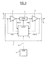
- FIG. 1 represents the structure of a first embodiment of an optical amplification device capable of implementing the invention.
- the device comprises a variable optical attenuator 4, the input of which is connected to an optical fiber 8 of a communication network.
- the input of an optical amplifier 3 is connected downstream of the output of the variable optical attenuator 4.
- the output of the optical amplifier 3 is connected to an optical fiber 9 of the communication network.
- the optical amplification device 1 also includes a controller 5, likely to control the variable optical attenuator 4 and the gain of the amplifier optical 3.
- the controller 5 is thus connected to the variable optical attenuator 4 and optical amplifier 3.
- Controller 5 also measures optical power Pin1 at the input of the variable optical attenuator 4, the optical powers Pin2 and Pout2 at the input and output of the optical amplifier 3.
- the controller 5 is preferably also connected to a control 7 via a network communication 6.
- the optical amplification device can quickly adapt the gain of the optical amplifier 3 without having to wait for confirmation of the change of the number of channels by an optical communication link. This avoids transient transmission problems when changing the number of channels to the input of the optical amplification device 1.
- the most frequent case of modification of the number of channels at the input comes from fiber breaks upstream of a optical multiplexer for insertion / extraction upstream of the amplification device optical 1.
- the number of channels can then suddenly be reduced, which causes a decrease in the input power Pin1 on the optical amplification device 1.
- Amplifier 3 is then adjusted to compensate for the reduction in power input Pin1 and keep the power per channel of the channels unchanged compared to the power per channel before the fiber breaks. All downstream amplifiers will perform this same gain adjustment operation by a chain effect.
- this device allows move from a fast communication network, which reduces the cost and overall complexity of the communication network.
- AttVOA variable optical attenuator
- FIG. 2 represents an amplification curve of the optical amplifier 3 showing the variations of its output power Pout2 (in dBm) as a function of the input power Pin2 (in dBm).
- the gain preferably has a first decreasing gain when the input power increases over a first range of input power, and a second substantially constant gain on a second input power range.
- the input powers on the first range are lower than the input powers on the second range, and the gain on the first range is greater than the gain on the second range. So, on the curve, the first range corresponds to part 10 and the second range corresponds to part 11.
- the gain remains substantially constant in the absence of determination of a change attenuation of the span.
- the power per channel at the output of the optical amplifier 3 then remains substantially constant.
- the gain increases.
- the output power is thus at a value sufficient to maintain a good signal-to-noise ratio when the power input drops. In this case the power per channel is no longer kept constant and increases.
- we can predict a gain on the first range such that the output power Pout2 of the amplifier is substantially constant on this range.
- FIG. 3 represents the structure of a second embodiment of an optical amplification device 1 capable of implementing the invention.
- the device 1 comprises an optical amplifier 2, the input of which is connected to an optical fiber 8.
- the input of a variable optical attenuator 4 is connected downstream of the output of the optical amplifier 2.
- the input of an optical amplifier 3 is connected downstream of the output of the variable optical attenuator 4.
- the output of the optical amplifier 3 is connected to an optical fiber 9.
- the optical amplification device 1 comprises a controller 5 similar to the controller of figure 1.
- the controller is thus able to control the attenuator variable optics 4 and the optical amplifiers 2 and 3.
- the controller 5 is thus connected to the variable optical attenuator 4 and to the optical amplifiers 3.
- the controller 5 measures the optical power Pin1 at the input of the optical amplifier 2, the optical power Pout1 at the output of the optical amplifier 2, the power Pin2 at the input of the optical amplifier 3 and the power Pout2 at the output of the optical amplifier 3.
- the controller 5 is preferably also connected to a control 7, similar to FIG. 1.
- variable optical attenuator 4 downstream of the amplifier optical 2 reduces signal losses at the input of the device optical amplification 1.
- the signal applied to the input of the device optical amplifier 1 is amplified by optical amplifier 2 before being applied to the variable optical attenuator 4.
- the loss on the signal intrinsic to a variable optical attenuator 4 is therefore only undergone after a prior step amplification.
- the optical amplification device 1 is therefore capable of amplifying signals with lower input powers, allowing to increase the distances between the different optical amplification devices 1 of the transmission network.
- the amplification of the optical amplifier 2 is preferably such that the power Pin1 is greater than the power Pin2 by at least 1 dB. So, the signal to noise ratio of the optical amplification device 1 is improved in the same report.
- the use of two optical amplifiers 2 and 3 makes it possible to maintain the spectral uniformity of the gain of the optical amplification device 1.
- the controller detects a variation in the attenuation of the span upstream of the amplification device 1 (variation of Pin1 without variation of the number of channels)
- amplification curves advantageously used in optical amplifiers 2 and 3. show the variations in the output powers Pout2 and Pout1 (in dBm) of optical amplifiers 2 and 3 respectively. function of the powers Pin2 and Pin1 (in dBm) received respectively on their inputs.
- the controller can modify the gains of the optical amplifiers 2 and 3, as a function of the number of channels at the input of the optical amplification device 1.
- the gain curve of the optical amplifier 2 preferably has a decreasing gain when the power Pin1 increases over a first power range.
- the gain curve of the optical amplifier 2 also preferably has a substantially constant gain over a second power range Fin1, the powers of the second range being greater than the powers of the first range. Gain on the first track is greater than the gain on the second track.
- the first power range corresponds to a Pout1 power substantially constant, while the second power range corresponds to a substantially constant gain.
- the gain curve of the optical amplifier 3 preferably has a decreasing gain when the Pin2 power increases over a first power range.
- the gain curve of the optical amplifier 3 also preferably has a substantially constant gain over a second power range Pin2, the powers of the second range being greater than the powers of the first range. Gain on the first track is greater than the gain on the second track.
- the first power range corresponds to a substantially constant Pout2 power
- the second power range corresponds to a substantially constant gain.
- This determination can be made either by external elements, such as that the control 7, arranged upstream of the amplification device and which provide device 1 with the Attspan attenuation value, either by device optical amplification 1 itself as a function of the number of channels supplied from of the information network 6.
- the optical amplification device 1 can determine the inter-amplifier attenuation by measuring Pin1 and then using either a reference value of the output power of the amplification device upstream, either by recovering this power value via the network 6.
- the controller may modify the value of AttVOA if a new value of AttSpan has been determined.
Landscapes
- Physics & Mathematics (AREA)
- Electromagnetism (AREA)
- Engineering & Computer Science (AREA)
- Computer Networks & Wireless Communication (AREA)
- Signal Processing (AREA)
- Optical Communication System (AREA)
- Lasers (AREA)
Applications Claiming Priority (2)
| Application Number | Priority Date | Filing Date | Title |
|---|---|---|---|
| FR0210141 | 2002-08-09 | ||
| FR0210141A FR2843505B1 (fr) | 2002-08-09 | 2002-08-09 | Dispositif d'amplification optique pour reseau optique a controle de gain automatique |
Publications (1)
| Publication Number | Publication Date |
|---|---|
| EP1388960A1 true EP1388960A1 (de) | 2004-02-11 |
Family
ID=30129729
Family Applications (1)
| Application Number | Title | Priority Date | Filing Date |
|---|---|---|---|
| EP03291960A Withdrawn EP1388960A1 (de) | 2002-08-09 | 2003-08-05 | Optischer Faserverstärker mit automatischer Verstärkungssteuerung |
Country Status (4)
| Country | Link |
|---|---|
| US (1) | US7016105B2 (de) |
| EP (1) | EP1388960A1 (de) |
| CN (1) | CN100420174C (de) |
| FR (1) | FR2843505B1 (de) |
Families Citing this family (11)
| Publication number | Priority date | Publication date | Assignee | Title |
|---|---|---|---|---|
| US7460296B2 (en) | 2002-04-30 | 2008-12-02 | Pivotal Decisions Llc | Compensation for spectral power tilt from scattering |
| US6977770B2 (en) * | 2002-06-14 | 2005-12-20 | Fujitsu Limited | Optical amplifier and control method therefor |
| EP1420491A3 (de) * | 2002-11-18 | 2005-04-27 | Fujitsu Limited | Optischer Verstärker und Verfahren zu dessen Regelung |
| US7466478B2 (en) * | 2002-12-19 | 2008-12-16 | Fujitsu Limited | Optical-level control method, optical-level control apparatus and wavelength-multiplexing optical network |
| JP3914236B2 (ja) * | 2003-01-30 | 2007-05-16 | 富士通株式会社 | 光増幅器 |
| EP1749355A1 (de) * | 2004-04-06 | 2007-02-07 | Bookham Technology plc | Voa-steuerelement |
| JP4707542B2 (ja) * | 2005-11-28 | 2011-06-22 | 富士通株式会社 | 伝送装置 |
| CN101043288B (zh) * | 2006-03-20 | 2011-09-21 | 中兴通讯股份有限公司 | 一种光复用层功率优化系统及其方法 |
| JP5239141B2 (ja) * | 2006-09-26 | 2013-07-17 | 富士通株式会社 | 光増幅装置およびその制御方法 |
| CN118414795A (zh) * | 2021-12-21 | 2024-07-30 | 日本电信电话株式会社 | 光通信控制装置、接收装置、通信系统及控制方法 |
| CN115333646B (zh) * | 2022-08-29 | 2023-07-28 | 云南保利天同水下装备科技有限公司 | 一种水声通讯器和其信号自动增益控制方法 |
Citations (3)
| Publication number | Priority date | Publication date | Assignee | Title |
|---|---|---|---|---|
| EP0975103A1 (de) * | 1998-02-06 | 2000-01-26 | Fujitsu Limited | Optischer verstärker, verfahren zur steuerung der lichtquellenerregung von einem optischen verstärker und verfahren zur steuerung des optischen verstärkers |
| EP1033834A2 (de) * | 1999-03-02 | 2000-09-06 | Fujitsu Limited | Optischer Verstärker und Optisches Übertragungssystem für Wellenlängenmultiplexübertragung |
| US6400479B1 (en) * | 1999-12-20 | 2002-06-04 | Sycamore Networks, Inc. | Optical power balancer for optical amplified WDM networks |
Family Cites Families (2)
| Publication number | Priority date | Publication date | Assignee | Title |
|---|---|---|---|---|
| DE19547603A1 (de) * | 1995-12-20 | 1997-06-26 | Sel Alcatel Ag | Optische Verstärkereinrichtung |
| KR100358115B1 (ko) * | 2000-12-14 | 2002-10-25 | 한국전자통신연구원 | 자동 이득 제어된 광섬유 증폭 장치 |
-
2002
- 2002-08-09 FR FR0210141A patent/FR2843505B1/fr not_active Expired - Fee Related
-
2003
- 2003-08-05 EP EP03291960A patent/EP1388960A1/de not_active Withdrawn
- 2003-08-06 CN CNB031497314A patent/CN100420174C/zh not_active Expired - Fee Related
- 2003-08-08 US US10/636,553 patent/US7016105B2/en not_active Expired - Fee Related
Patent Citations (3)
| Publication number | Priority date | Publication date | Assignee | Title |
|---|---|---|---|---|
| EP0975103A1 (de) * | 1998-02-06 | 2000-01-26 | Fujitsu Limited | Optischer verstärker, verfahren zur steuerung der lichtquellenerregung von einem optischen verstärker und verfahren zur steuerung des optischen verstärkers |
| EP1033834A2 (de) * | 1999-03-02 | 2000-09-06 | Fujitsu Limited | Optischer Verstärker und Optisches Übertragungssystem für Wellenlängenmultiplexübertragung |
| US6400479B1 (en) * | 1999-12-20 | 2002-06-04 | Sycamore Networks, Inc. | Optical power balancer for optical amplified WDM networks |
Also Published As
| Publication number | Publication date |
|---|---|
| CN1481104A (zh) | 2004-03-10 |
| FR2843505B1 (fr) | 2006-06-02 |
| US7016105B2 (en) | 2006-03-21 |
| US20040027651A1 (en) | 2004-02-12 |
| CN100420174C (zh) | 2008-09-17 |
| FR2843505A1 (fr) | 2004-02-13 |
Similar Documents
| Publication | Publication Date | Title |
|---|---|---|
| US6798567B2 (en) | Method and apparatus for controlling power transients in an optical communication system | |
| FR2756994A1 (fr) | Egaliseur optique | |
| FR2775856A1 (fr) | Systeme et terminal de multiplexage en longueur d'onde optique | |
| EP1388960A1 (de) | Optischer Faserverstärker mit automatischer Verstärkungssteuerung | |
| FR2753284A1 (fr) | Amplificateur optique et procede d'amplification optique | |
| EP0881790B1 (de) | Optisches Übertragungssystem mit dynamischer Kompensation der übertragenen Leistung | |
| EP1376904A1 (de) | Optischer Verstärker und Steuerverfahren dafür | |
| US20040037564A1 (en) | Method and system for span optical power control | |
| US7612936B2 (en) | Optical amplifying apparatus for wavelength division multiplexed signals | |
| US7657187B2 (en) | Optical transmission apparatus and optical transmission control method for wavelength-division-multiplexed optical signal | |
| US7619813B2 (en) | Wavelength division multiplexing device, an optical leakage prevention method, and a wavelength division multiplexing communication system | |
| US6490080B2 (en) | Gain controlled optically pre-amplified receiver apparatus and method | |
| FR2820570A1 (fr) | Systeme et procede de transmission optique | |
| FR2832274A1 (fr) | Procede de controle dynamique d'un module optique | |
| FR2859054A1 (fr) | Controle dynamique de perte de puissance dans une fibre optique par contrapropagation d'un canal de supervision | |
| EP1355141A2 (de) | Vorrichtung zur Messung und dynamischen Kompensation der Variation von Leistungsverlust in einer optischen Transmissionsleitung mit Supervisionskanal und zugehöriges Verfahren | |
| US7061670B2 (en) | Optical fiber amplifier having automatic power control function and automatic power control method | |
| EP1353458B1 (de) | Vorrichtung zur Messung und/oder zur dynamischen Kontrolle von Verlustleistung in einer optischen Übertragungsleitung und zugehöriges Verfahren | |
| EP0598651B1 (de) | Optisches Übertragungssystem, insbesondere für ein Videokommunikationskabelnetzwerk | |
| US7054515B1 (en) | Diffractive light modulator-based dynamic equalizer with integrated spectral monitor | |
| EP0037857B1 (de) | Verfahren zur Übertragung analoger Information über Lichtleitfasern und Anlage zur Durchführung des Verfahrens | |
| JP4693864B2 (ja) | 波長多重光装置及び波長多重光通信システム | |
| FR2687867A1 (fr) | Ensemble formant preamplificateur et recepteur optique, et procede d'optimisation de sa sensibilite. | |
| FR2901937A1 (fr) | Systeme de transmission optique avec ajustement de gain | |
| KR20010048176A (ko) | 파장분할 다중화 시스템의 채널 광출력 자동 조정장치 |
Legal Events
| Date | Code | Title | Description |
|---|---|---|---|
| PUAI | Public reference made under article 153(3) epc to a published international application that has entered the european phase |
Free format text: ORIGINAL CODE: 0009012 |
|
| AK | Designated contracting states |
Kind code of ref document: A1 Designated state(s): AT BE BG CH CY CZ DE DK EE ES FI FR GB GR HU IE IT LI LU MC NL PT RO SE SI SK TR |
|
| AX | Request for extension of the european patent |
Extension state: AL LT LV MK |
|
| 17P | Request for examination filed |
Effective date: 20040811 |
|
| AKX | Designation fees paid |
Designated state(s): AT BE BG CH CY CZ DE DK EE ES FI FR GB GR HU IE IT LI LU MC NL PT RO SE SI SK TR |
|
| RAP1 | Party data changed (applicant data changed or rights of an application transferred) |
Owner name: ALCATEL LUCENT |
|
| STAA | Information on the status of an ep patent application or granted ep patent |
Free format text: STATUS: THE APPLICATION IS DEEMED TO BE WITHDRAWN |
|
| 18D | Application deemed to be withdrawn |
Effective date: 20100302 |