EP1411583A1 - Radar apparatus - Google Patents
Radar apparatus Download PDFInfo
- Publication number
- EP1411583A1 EP1411583A1 EP20030023630 EP03023630A EP1411583A1 EP 1411583 A1 EP1411583 A1 EP 1411583A1 EP 20030023630 EP20030023630 EP 20030023630 EP 03023630 A EP03023630 A EP 03023630A EP 1411583 A1 EP1411583 A1 EP 1411583A1
- Authority
- EP
- European Patent Office
- Prior art keywords
- dielectric resonator
- cover
- frequency
- facing
- oscillator
- Prior art date
- Legal status (The legal status is an assumption and is not a legal conclusion. Google has not performed a legal analysis and makes no representation as to the accuracy of the status listed.)
- Withdrawn
Links
Images




Classifications
-
- H—ELECTRICITY
- H01—ELECTRIC ELEMENTS
- H01P—WAVEGUIDES; RESONATORS, LINES, OR OTHER DEVICES OF THE WAVEGUIDE TYPE
- H01P1/00—Auxiliary devices
- H01P1/20—Frequency-selective devices, e.g. filters
- H01P1/207—Hollow waveguide filters
- H01P1/211—Waffle-iron filters; Corrugated structures
-
- H—ELECTRICITY
- H10—SEMICONDUCTOR DEVICES; ELECTRIC SOLID-STATE DEVICES NOT OTHERWISE PROVIDED FOR
- H10W—GENERIC PACKAGES, INTERCONNECTIONS, CONNECTORS OR OTHER CONSTRUCTIONAL DETAILS OF DEVICES COVERED BY CLASS H10
- H10W42/00—Arrangements for protection of devices
- H10W42/20—Arrangements for protection of devices protecting against electromagnetic or particle radiation, e.g. light, X-rays, gamma-rays or electrons
-
- G—PHYSICS
- G01—MEASURING; TESTING
- G01S—RADIO DIRECTION-FINDING; RADIO NAVIGATION; DETERMINING DISTANCE OR VELOCITY BY USE OF RADIO WAVES; LOCATING OR PRESENCE-DETECTING BY USE OF THE REFLECTION OR RERADIATION OF RADIO WAVES; ANALOGOUS ARRANGEMENTS USING OTHER WAVES
- G01S7/00—Details of systems according to groups G01S13/00, G01S15/00, G01S17/00
- G01S7/02—Details of systems according to groups G01S13/00, G01S15/00, G01S17/00 of systems according to group G01S13/00
- G01S7/03—Details of HF subsystems specially adapted therefor, e.g. common to transmitter and receiver
- G01S7/032—Constructional details for solid-state radar subsystems
-
- H—ELECTRICITY
- H10—SEMICONDUCTOR DEVICES; ELECTRIC SOLID-STATE DEVICES NOT OTHERWISE PROVIDED FOR
- H10W—GENERIC PACKAGES, INTERCONNECTIONS, CONNECTORS OR OTHER CONSTRUCTIONAL DETAILS OF DEVICES COVERED BY CLASS H10
- H10W72/00—Interconnections or connectors in packages
- H10W72/071—Connecting or disconnecting
- H10W72/075—Connecting or disconnecting of bond wires
-
- H—ELECTRICITY
- H10—SEMICONDUCTOR DEVICES; ELECTRIC SOLID-STATE DEVICES NOT OTHERWISE PROVIDED FOR
- H10W—GENERIC PACKAGES, INTERCONNECTIONS, CONNECTORS OR OTHER CONSTRUCTIONAL DETAILS OF DEVICES COVERED BY CLASS H10
- H10W72/00—Interconnections or connectors in packages
- H10W72/50—Bond wires
- H10W72/551—Materials of bond wires
-
- H—ELECTRICITY
- H10—SEMICONDUCTOR DEVICES; ELECTRIC SOLID-STATE DEVICES NOT OTHERWISE PROVIDED FOR
- H10W—GENERIC PACKAGES, INTERCONNECTIONS, CONNECTORS OR OTHER CONSTRUCTIONAL DETAILS OF DEVICES COVERED BY CLASS H10
- H10W72/00—Interconnections or connectors in packages
- H10W72/90—Bond pads, in general
- H10W72/951—Materials of bond pads
-
- H—ELECTRICITY
- H10—SEMICONDUCTOR DEVICES; ELECTRIC SOLID-STATE DEVICES NOT OTHERWISE PROVIDED FOR
- H10W—GENERIC PACKAGES, INTERCONNECTIONS, CONNECTORS OR OTHER CONSTRUCTIONAL DETAILS OF DEVICES COVERED BY CLASS H10
- H10W90/00—Package configurations
- H10W90/701—Package configurations characterised by the relative positions of pads or connectors relative to package parts
- H10W90/751—Package configurations characterised by the relative positions of pads or connectors relative to package parts of bond wires
- H10W90/753—Package configurations characterised by the relative positions of pads or connectors relative to package parts of bond wires between laterally-adjacent chips
-
- H—ELECTRICITY
- H10—SEMICONDUCTOR DEVICES; ELECTRIC SOLID-STATE DEVICES NOT OTHERWISE PROVIDED FOR
- H10W—GENERIC PACKAGES, INTERCONNECTIONS, CONNECTORS OR OTHER CONSTRUCTIONAL DETAILS OF DEVICES COVERED BY CLASS H10
- H10W90/00—Package configurations
- H10W90/701—Package configurations characterised by the relative positions of pads or connectors relative to package parts
- H10W90/751—Package configurations characterised by the relative positions of pads or connectors relative to package parts of bond wires
- H10W90/754—Package configurations characterised by the relative positions of pads or connectors relative to package parts of bond wires between a chip and a stacked insulating package substrate, interposer or RDL
Definitions
- the present invention relates to a radar apparatus.
- An automotive radar using millimeter wave, or a high-frequency radio communication apparatus and radio terminal using waves in a frequency band of 300 MHz or above contain a single multifunctional semiconductor device, a semiconductor integrated circuit (IC), an IC package which packages the ICs, a plurality of interconnected ICs or a high-frequency circuit element having a filter function in a housing. This is for the miniaturization, and cost reduction of the apparatuses, and to cope with multi-functionalization of the circuit element to be used.
- IC semiconductor integrated circuit
- the size of the housing When packing many functional devices in one housing structure, if the size of the housing remains constant and the number of the functional devices increases, the physical distance between the functional devices will be decreased correspondingly, or the size of the housing will be larger than half the free-space wavelength at a signal frequency (for example, about 1.95mm at 77GHz). In either case, radio energy of a signal frequency radiated from one point of IC or the like constituting a functional device within the housing is easily dissipated in the housing, and combines with a functional device within the same housing, thus causing various functional troubles.
- a signal frequency for example, about 1.95mm at 77GHz
- a communication transmitter-receiver or a transmitter-receiver module for automotive millimeter wave radar experiences a trouble such as the saturation of a receiver, an increase in received noise or the like.
- a conventional communication apparatus has divided the housing structure into a plurality of small rooms by metal partitions, or has provided a metal structure along a conventional communication path that serves as a cutoff waveguide structure for locally cutting off unnecessary irradiation.
- These conventional techniques require a complicated metal structure for the housing structure, and a division of high-frequency board of a passive circuit into a plurality of parts. Further, these structures and the division of the high-frequency board into a plurality of parts make the arrangement of semiconductor ICs and the passive circuit components more difficult, thus inhibiting mass production and cost reduction of the communication apparatus.
- JP-A-2000-307305 is among the conventional techniques for solving there problems.
- JP-A-2000-307305 proposes a mounting configuration in which a filter has a lid formed with projections by extrusion press
- the invention does not refer to a relative positional relationship between the projections and the high-frequency circuit elements or passive components, and an optimal configuration of the projections on those positions.
- a dielectric resonator is generally used as an oscillator which is a high-frequency circuit element.
- Oscillation frequency of the oscillator changes a lot depending on the dielectric resonator and electric field conditions in the vicinity of the dielectric resonator.
- the oscillation frequency changes a lot depending on the shape and position of the projections, thereby making it very difficult to acquire a desired oscillation frequency.
- the projections are formed by press working, if the projections diminish in size, increase in height, or increase in number, pressing load is increased and thus the life of a press mold will be shortened. Therefore, it is necessary to arrange projections of optimal shape and height only at required places on the lid.
- a car-mounted radar apparatus comprising a dielectric resonator and/or a high-frequency oscillator connected to the dielectric resonator for generating a high-frequency.
- a cover for covering a base, where the dielectric resonator and/or the high-frequency oscillator are deposited, and the dielectric resonator and/or high-frequency oscillator with a space therebetween may be provided.
- the distance between the resonator and/or the high-frequency oscillator and the cover may be a quarter or over of the effective wave length of the high-frequency oscillator.
- a radar apparatus comprising a dielectric resonator, a high-frequency oscillator connected to the dielectric resonator, a base on which the dielectric resonator and high-frequency oscillator are mounted and/or a cover bonded to the base for covering the dielectric resonator and high-frequency oscillator.
- the distance between the surface of the cover facing the dielectric resonator and the surface of the base facing the dielectric resonator may be half or below of the effective wave length of the oscillator frequency.
- the cover can have periodic projections facing the dielectric resonator which are a quarter of the effective wave length of the oscillator frequency.
- the nearest distance between the surface of the dielectric resonator facing the cover and the surface of the cover facing the dielectric resonator may be a quarter or over of the effective wave length of the oscillator frequency.
- a radar apparatus comprising an MMIC that includes an oscillator, an amplifier and a mixer, a circuit board on which the MMIC is mounted and connected, an antenna board on which antennae are mounted, a base on which the circuit board and the antenna board are mounted and/or a coaxial cable or waveguide which passes through the base and connects the circuit board and antenna board.
- a cover which is bonded to the base to cover the MMIC and circuit board may be provided with projections facing the MMIC and circuit board. At least any of the pitch, size, and shape of the projections formed on a place of the cover unit facing the coaxial cable or waveguide may differ from that of the projections formed on other place than the foregoing of the cover unit.
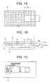
- Fig. 1 shows oscillation unit of a high-frequency module, which comprises a dielectric resonator 1, a high-frequency oscillator 2 connected to the dielectric resonator 1, a base 3 where the dielectric resonator 1 and high-frequency oscillator 2 are mounted, and a cover unit 4 bonded to the base 3 for covering the dielectric resonator 1 and high-frequency oscillator 2, wherein the distance H between the surface of the cover unit 4 facing the dielectric resonator 1 and the surface of the base 3 facing the dielectric resonator 1 is half or below of the effective wave length of the frequency of the oscillator 2, and the cover unit 4 has periodic projections 5 facing the dielectric resonator 1 which have a length L, a quarter of the effective wave length of frequency of the oscillator 2.
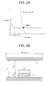
- Fig. 2A shows that resonance frequency f0 changes as the distance M between a dielectric resonator and an outer wall 11 changes.
- a graph of solid line in Fig 2A shows that sensitivity of resonance frequency relative to M begins to decrease from about one eighth of wavelength at resonance frequency f0, and there is no sensitivity at about a quarter of wavelength. Further, a graph of broken line shows a cut off frequency relative to M. A point P shows that the frequency of the dielectric resonator 1 just matches the cut off frequency, and if M is not smaller than a value represented by the point P, a noise level at the frequency band f0 will rise.
- projections 5 are not formed on at least a portion of the cover unit 4 facing the dielectric resonator 1.
- H is set to be a little bit smaller than 1/2 ⁇
- the height of the dielectric resonator 1 is generally smaller than 1/4 ⁇ 0
- the distance between the dielectric resonator 1 and the cover unit 4 becomes 1/4 ⁇ 0 ⁇ M
- the oscillation frequency does not change depending on the presence or absence of the filter cover unit 4.
- desired oscillation frequency is easily acquired, and since frequency band at f0 is cut off frequency or below, it is possible to suppress the noise level.
- this filter cover structure is highly superior.
- X and Y of the portion where the intrusions 5 are not formed are far enough from the frequency f1 acquired from the following expression (1) such that they do not resonate with f0 as a cavity resonator.
- f1 C/2 ⁇ ( (m/X) 2 + (n/Y) 2 + (s/H) 2 )
- m, n, s resonation mode
- the shape of the dielectric resonator is not necessarily square, and a round or a just polygonal shape is acceptable.
- a wave absorber 12 When a wave absorber 12 is mounted on a portion as shown in Figs. 3A, and 3B that corresponds to that in Figs. 1A and 1B where projections were not formed, it can compensate the filter characteristics that were lost due to the lack of the projections 5, and frequency variation caused by the cover unit 4 is minimized. Thus, it can be said that the filter structure is highly superior.
- the filter structure is highly superior.
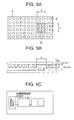
- deterioration of filter characteristics is prevented and frequency variation caused by the cover unit 4 is minimized by forming projections 52 as shown in Fig. 5A, which are smaller in shape than other projections, on portions corresponding to those in Fig. 1A where projections 5 were not formed.
- projections 52 as shown in Fig. 5A, which are smaller in shape than other projections, on portions corresponding to those in Fig. 1A where projections 5 were not formed.
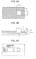
- the filter cover unit structure 4 whose filter characteristics are provided by wave absorber 12 instead of projections with reference to Figs. 6A, and 6B.
- the wave absorbers 12 formed on a portion corresponding to that in Fig. 1, where projections 5 are not formed are taken out as shown in the Figs. 6A and 6B.
- a filter cover unit having the same effect with that in Fig. 1A and 1B can be provided.
- a material or a structure, that absorbs electric wave better than the cover unit 4, is used for the wave absorber 12.
- the filter cover structure is highly superior.
- the filter structure is highly superior.
- Fig. 8 shows a transmitter-receiver. It comprises a MMIC (Monolithic Microwave Integrated Circuit) including an oscillator 2, an amplifier 6, and a mixer 7, a circuit board 8 where the MMIC is mounted and connected, an antenna board 9 where antennae are disposed, a base 3 where a coaxial cable 10 or a waveguide, which passes through the base to connect the circuit board 8, and antenna board 9 are held, and a cover unit 4 which is bonded to the base 3 to cover the MMIC and circuit board 8 and is provided with projections 5 on the side thereof facing the MMIC and circuit board 8.
- MMIC Monitoring Microwave Integrated Circuit
- the projections 5 are formed by press working. As the projections reduce in size, increase in height, or increase in number thereof, a pressing load increases correspondingly and thereby shortens the life of a press mold. Therefore, projections must be formed that have an optimum shape and height only at necessary locations on the cover unit 4.
- the pitch, size and shape of projections formed on a place of the cover unit 4 that faces the coaxial cable 10 or waveguide are changed from those of the projections formed on other place of the cover unit 4 than the forgoing place as shown by projections 51 and 52 in Fig. 9.
- Projections 51 0.5mm x 0.8mm
- Projections 52 0.7mm x 0.8mm
- the pitch, size, and shape of the projections formed on a place of the cover unit 4 that faces the coaxial cable (transmission side) 101 - coaxial cable (reception side) 102 are changed from those of the projections formed on a place of the cover unit 4 that faces a coaxial cable (reception side A) 1021 - coaxial cable (reception side B) 1022, as shown by projections 51 and 52 in Fig. 10.
- the isolation level required between the coaxial cable (transmission side) 101 and the coaxial cable (reception side) 102 differs from that required between the coaxial cable (transmission side A) 1021 and coaxial cable (reception side B) 1022.
- isolation can be secured even in a short distance by forming smaller projections 51 on a place of the cover unit 4 that faces the coaxial cable (reception side A) 1021 - coaxial cable (reception side B) 1022. Further, the life of the press mold can be lengthened by forming larger projections 52 on a place of the cover unit 4 that faces the coaxial cable (transmission side) 101 - the coaxial cable (reception side) 102. Thus, it can be said that the filter cover structure is highly superior.
- Projection 51 0.5mm x 0.8mm
- Projection 52 0.7mm x 0.8mm
- the wave absorber 121 a material having high wave absorptivity
- a wave absorber 122 a material having low absorptivity
- the wave absorbers are efficiently used, since a material having high absorptivity is generally expensive.
- the filter cover structure is highly superior.
- a car-mounted radar using the transmitter-receiver shown in Fig. 8 with reference to Figs. 13 and 14. Its structure will be described with reference to Fig. 13.
- Power is supplied from a connector 50 to a signal processing circuit 51, and the signal processing circuit 51, at the same time, supplies predetermined power to the transmitter - receiver 59 via a cable 52.
- an oscillator 53 generates millimeter wave of 76.5GHz, which is amplified by an amplifier 54 and fed to a transmission antenna 57 via a coaxial cable 56. Millimeter wave is transmitted from the transmission antenna 57, and the reception antenna 58 receives reflected wave after striking a target.
- Received wave is down-converted with transmission wave by a mixer 55, and transmitted as an IF signal to the signal processing circuit 51 via the cable 52.
- a relative speed, a distance, an angle and the like between a car or the like on which the radar is mounted and a target are calculated. These results are outputted via the connector 50.
- a car-mounted radar comprises a antenna unit including a transmission antenna 57 and reception antennae 581, 582, a high-frequency wave unit, and a control unit.
- the high-frequency unit has a transmission function for outputting a high-frequency signal, which is outputted by the oscillator 53 and amplified by the amplifier 54, to a space in front of a car via the antenna 57, and a reception function for extracting a Doppler signal which is acquired by down-converting a reflected wave from a target that is received by the reception antenna 531, 582 and an output signal of the oscillator 53 by the mixers 551, 552.
- the oscillator 53, amplifier 54, mixers 551, 552 comprise an integrated circuit such as MMIC (Monolithic Microwave Integrated Circuit) or the like.
- the control unit digitizes a Doppler frequency which the high-frequency unit outputted in a signal processing circuit 51, and then calculates a distance, a relative speed, and an angle to a target by signal processing based on various algorithms. Further, a power source unit 60 in the control unit has a function to supply bias supply to each MMIC of the high-frequency unit.
Landscapes
- Radar Systems Or Details Thereof (AREA)
- Control Of Motors That Do Not Use Commutators (AREA)
- Waveguides (AREA)
Abstract
The invention refers to a filter cover (4) which has
little electromagnetic effect on a dielectric resonator (1)
and is able to lengthen the life of a press mold without
impairing isolation between transmission and reception. A VCO
comprising a dielectric resonator (1), a high-frequency
oscillator (2), a base (3), a cover (4), in which the
distance between the surface of the cover (4) facing the
dielectric resonator (1) and the surface of the base (3)
facing the dielectric resonator (1) is half or below of the
effective wave length of the oscillator frequency, and the
cover (4) has periodic projections (5) facing the dielectric
resonator (1) which are a quarter of effective wave length of
the oscillator frequency, wherein the nearest distance M
between the surface of the dielectric resonator (1) facing
the cover (4) and the surface of the cover (4) facing the
dielectric resonator (1) is a quarter or over of the
effective wave length of the oscillator frequency.


Description
- The present invention relates to a radar apparatus.
- An automotive radar using millimeter wave, or a high-frequency radio communication apparatus and radio terminal using waves in a frequency band of 300 MHz or above contain a single multifunctional semiconductor device, a semiconductor integrated circuit (IC), an IC package which packages the ICs, a plurality of interconnected ICs or a high-frequency circuit element having a filter function in a housing. This is for the miniaturization, and cost reduction of the apparatuses, and to cope with multi-functionalization of the circuit element to be used.
- When packing many functional devices in one housing structure, if the size of the housing remains constant and the number of the functional devices increases, the physical distance between the functional devices will be decreased correspondingly, or the size of the housing will be larger than half the free-space wavelength at a signal frequency (for example, about 1.95mm at 77GHz). In either case, radio energy of a signal frequency radiated from one point of IC or the like constituting a functional device within the housing is easily dissipated in the housing, and combines with a functional device within the same housing, thus causing various functional troubles. For example, if part of signals emitted from a transmission function device into the housing is coupled with a reception functional device, a communication transmitter-receiver or a transmitter-receiver module for automotive millimeter wave radar experiences a trouble such as the saturation of a receiver, an increase in received noise or the like.
- To cope with these problems, especially an interference problem in the housing, a conventional communication apparatus has divided the housing structure into a plurality of small rooms by metal partitions, or has provided a metal structure along a conventional communication path that serves as a cutoff waveguide structure for locally cutting off unnecessary irradiation. These conventional techniques require a complicated metal structure for the housing structure, and a division of high-frequency board of a passive circuit into a plurality of parts. Further, these structures and the division of the high-frequency board into a plurality of parts make the arrangement of semiconductor ICs and the passive circuit components more difficult, thus inhibiting mass production and cost reduction of the communication apparatus.
- JP-A-2000-307305 is among the conventional techniques for solving there problems.
- However, while the prevention in JP-A-2000-307305 proposes a mounting configuration in which a filter has a lid formed with projections by extrusion press, the invention does not refer to a relative positional relationship between the projections and the high-frequency circuit elements or passive components, and an optimal configuration of the projections on those positions.
- However, a dielectric resonator is generally used as an oscillator which is a high-frequency circuit element. Oscillation frequency of the oscillator changes a lot depending on the dielectric resonator and electric field conditions in the vicinity of the dielectric resonator. Thus, if there exist projections which are extrusion-pressed on the lid in the vicinity of the dielectric resonator, the oscillation frequency changes a lot depending on the shape and position of the projections, thereby making it very difficult to acquire a desired oscillation frequency.
- Since the projections are formed by press working, if the projections diminish in size, increase in height, or increase in number, pressing load is increased and thus the life of a press mold will be shortened. Therefore, it is necessary to arrange projections of optimal shape and height only at required places on the lid.
- It is an object of the present invention to provide a filter cover that has little electromagnetic effect on the dielectric resonator. It is another object to lengthen the life of the press mold without injuring isolation between transmission and reception.
- The above object is achieved by a car-mounted radar apparatus comprising a dielectric resonator and/or a high-frequency oscillator connected to the dielectric resonator for generating a high-frequency. A cover for covering a base, where the dielectric resonator and/or the high-frequency oscillator are deposited, and the dielectric resonator and/or high-frequency oscillator with a space therebetween may be provided. The distance between the resonator and/or the high-frequency oscillator and the cover may be a quarter or over of the effective wave length of the high-frequency oscillator.
- The above object is also achieved by a radar apparatus comprising a dielectric resonator, a high-frequency oscillator connected to the dielectric resonator, a base on which the dielectric resonator and high-frequency oscillator are mounted and/or a cover bonded to the base for covering the dielectric resonator and high-frequency oscillator. The distance between the surface of the cover facing the dielectric resonator and the surface of the base facing the dielectric resonator may be half or below of the effective wave length of the oscillator frequency. The cover can have periodic projections facing the dielectric resonator which are a quarter of the effective wave length of the oscillator frequency. The nearest distance between the surface of the dielectric resonator facing the cover and the surface of the cover facing the dielectric resonator may be a quarter or over of the effective wave length of the oscillator frequency.
- The above object is also achieved by a radar apparatus comprising an MMIC that includes an oscillator, an amplifier and a mixer, a circuit board on which the MMIC is mounted and connected, an antenna board on which antennae are mounted, a base on which the circuit board and the antenna board are mounted and/or a coaxial cable or waveguide which passes through the base and connects the circuit board and antenna board.
- A cover which is bonded to the base to cover the MMIC and circuit board may be provided with projections facing the MMIC and circuit board. At least any of the pitch, size, and shape of the projections formed on a place of the cover unit facing the coaxial cable or waveguide may differ from that of the projections formed on other place than the foregoing of the cover unit.
- Other objects, features and advantages of the invention will become apparent from the following description of the embodiments of the invention taken in conjunction with the accompanying drawings.
-
- Figs. 1A to 1C are diagrams showing a first embodiment according to the present invention;
- Figs. 2A and 2B are a graph and a diagram, respectively, for complementing the first embodiment according to the present invention;
- Figs. 3A to 3C are diagrams showing an application example 1 of the first embodiment according to the present invention;
- Figs. 4A to 4C are diagrams showing an application example 2 of the first embodiment according to the present invention;
- Figs. 5A to 5C are diagrams showing an application example 3 of the first embodiment according to the present invention;
- Figs. 6A to 6C are diagrams showing an application example 4 of the first embodiment according to the present invention;
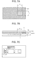
- Figs. 7A to 7C are diagrams showing an application example 5 of the first embodiment according to the present invention;
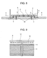
- Fig. 8 is a view showing a second embodiment according to the present invention;
- Fig. 9 is an enlarged view of a section A in Fig. 8;
- Fig. 10 is a sectional view taken along B - B in Fig. 8;
- Fig. 11 is an enlarged view A in Fig. 8;
- Fig. 12 is a sectional view taken along B - B in Fig. 8;
- Fig. 13 a structural view showing a car-mounted radar using a transmitter-receiver according to the present invention; and
- Fig. 14 is a circuit diagram for a car-mounted radar using a transmitter-receiver according to the present invention.
-
- A radar apparatus according to the present invention will be described with reference to Fig. 1.
- Fig. 1 shows oscillation unit of a high-frequency module, which comprises a
dielectric resonator 1, a high-frequency oscillator 2 connected to thedielectric resonator 1, abase 3 where thedielectric resonator 1 and high-frequency oscillator 2 are mounted, and acover unit 4 bonded to thebase 3 for covering thedielectric resonator 1 and high-frequency oscillator 2, wherein the distance H between the surface of thecover unit 4 facing thedielectric resonator 1 and the surface of thebase 3 facing thedielectric resonator 1 is half or below of the effective wave length of the frequency of theoscillator 2, and thecover unit 4 hasperiodic projections 5 facing thedielectric resonator 1 which have a length L, a quarter of the effective wave length of frequency of theoscillator 2. - Fig. 2A and 2B will be described.
- Fig. 2A shows that resonance frequency f0 changes as the distance M between a dielectric resonator and an
outer wall 11 changes. - A graph of solid line in Fig 2A shows that sensitivity of resonance frequency relative to M begins to decrease from about one eighth of wavelength at resonance frequency f0, and there is no sensitivity at about a quarter of wavelength. Further, a graph of broken line shows a cut off frequency relative to M. A point P shows that the frequency of the
dielectric resonator 1 just matches the cut off frequency, and if M is not smaller than a value represented by the point P, a noise level at the frequency band f0 will rise. - Therefore, preferably, 1/4λ0≦M, H≦λ.
- Now, return to Fig. 1.
- Here, note that
projections 5 are not formed on at least a portion of thecover unit 4 facing thedielectric resonator 1. At this time, since H is set to be a little bit smaller than 1/2λ, and the height of thedielectric resonator 1 is generally smaller than 1/4λ0, the distance between thedielectric resonator 1 and thecover unit 4 becomes 1/4λ0≦M, and the oscillation frequency does not change depending on the presence or absence of thefilter cover unit 4. Further, desired oscillation frequency is easily acquired, and since frequency band at f0 is cut off frequency or below, it is possible to suppress the noise level. Thus, it can be said that this filter cover structure is highly superior. It should be noted that the dimensions of X and Y of the portion where theintrusions 5 are not formed are far enough from the frequency f1 acquired from the following expression (1) such that they do not resonate with f0 as a cavity resonator. - Specific dimensions are as below;
Dimension of the dielectric resonator 1 :
□1.32mm × 0.53mm
H=1.9mm
L=0.9mm
M=1.9-0.53=1.37mm
X=3.5mm
f0=76.5GHz λ0=3.9mm - However, the shape of the dielectric resonator is not necessarily square, and a round or a just polygonal shape is acceptable.
- When a
wave absorber 12 is mounted on a portion as shown in Figs. 3A, and 3B that corresponds to that in Figs. 1A and 1B where projections were not formed, it can compensate the filter characteristics that were lost due to the lack of theprojections 5, and frequency variation caused by thecover unit 4 is minimized. Thus, it can be said that the filter structure is highly superior. - Further, the deterioration of filter characteristics is prevented and frequency variation caused by the
cover unit 4 is minimized by forming afew projections 51 as shown in Figs. 4A and 4B, while satisfying 1/4λ≦M. Thus, it can be said that the filter structure is highly superior. - Further, deterioration of filter characteristics is prevented and frequency variation caused by the
cover unit 4 is minimized by formingprojections 52 as shown in Fig. 5A, which are smaller in shape than other projections, on portions corresponding to those in Fig. 1A whereprojections 5 were not formed. Thus, it can be said that the filter structure is highly superior. - Next, description will be given of the filter
cover unit structure 4 whose filter characteristics are provided bywave absorber 12 instead of projections with reference to Figs. 6A, and 6B. In this case, if thedielectric resonator 1 is near to thewave absorber 12, oscillation frequency also changes a lot depending on the presence or absence of thefilter cover 4. Therefore, to cope with this, thewave absorbers 12 formed on a portion corresponding to that in Fig. 1, whereprojections 5 are not formed, are taken out as shown in the Figs. 6A and 6B. With this, a filter cover unit having the same effect with that in Fig. 1A and 1B can be provided. Here, a material or a structure, that absorbs electric wave better than thecover unit 4, is used for thewave absorber 12. - Further, the deterioration of filter characteristics is prevented and the frequency variation caused by the
cover unit 4 is minimized by satisfying 1/4λ≦M while forming afew wave absorbers 121, as shown by Figs. 7A and 7B, on a portion corresponding to a portion in Fig. 1A where theprojections 5 are not formed. Thus, it can be said the filter cover structure is highly superior. Thus, it can be said that the filter structure is highly superior. - Another
filter cover unit 4 according to the present invention will be described with reference to Fig. 8. - Fig. 8 shows a transmitter-receiver. It comprises a MMIC (Monolithic Microwave Integrated Circuit) including an
oscillator 2, anamplifier 6, and amixer 7, acircuit board 8 where the MMIC is mounted and connected, anantenna board 9 where antennae are disposed, abase 3 where acoaxial cable 10 or a waveguide, which passes through the base to connect thecircuit board 8, andantenna board 9 are held, and acover unit 4 which is bonded to thebase 3 to cover the MMIC andcircuit board 8 and is provided withprojections 5 on the side thereof facing the MMIC andcircuit board 8. - The
projections 5 are formed by press working. As the projections reduce in size, increase in height, or increase in number thereof, a pressing load increases correspondingly and thereby shortens the life of a press mold. Therefore, projections must be formed that have an optimum shape and height only at necessary locations on thecover unit 4. - Here, the pitch, size and shape of projections formed on a place of the
cover unit 4 that faces thecoaxial cable 10 or waveguide are changed from those of the projections formed on other place of thecover unit 4 than the forgoing place as shown byprojections - Although unwanted electric wave is irradiated, at this time, due to unmatched impedance at a converting portion of a transmission path from the
coaxial cable 10 or waveguide to thecircuit board 8, the dissipation of the unwanted electric wave is suppressed by formingsmaller projections 51 at a place of thecover unit 4 that face thecoaxial cable 10 or waveguide. At the same time,larger projections 52 are formed on a place of thecover unit 4 other than the foregoing one, thus making it possible to lengthen the life of the press mold. It can be said that the filter cover structure is highly superior. - Specific dimensions are as below;
Projections 51: 0.5mm x 0.8mm
Projections 52: 0.7mm x 0.8mm - Further, the pitch, size, and shape of the projections formed on a place of the
cover unit 4 that faces the coaxial cable (transmission side) 101 - coaxial cable (reception side) 102 are changed from those of the projections formed on a place of thecover unit 4 that faces a coaxial cable (reception side A) 1021 - coaxial cable (reception side B) 1022, as shown byprojections - Since the level of power radiated from the coaxial cable (transmission side) 101 differs from the level of power radiated from the coaxial cable (reception side) 102, and the distance between the each cable also differs, the isolation level required between the coaxial cable (transmission side) 101 and the coaxial cable (reception side) 102 differs from that required between the coaxial cable (transmission side A) 1021 and coaxial cable (reception side B) 1022.
- At this time, isolation can be secured even in a short distance by forming
smaller projections 51 on a place of thecover unit 4 that faces the coaxial cable (reception side A) 1021 - coaxial cable (reception side B) 1022. Further, the life of the press mold can be lengthened by forminglarger projections 52 on a place of thecover unit 4 that faces the coaxial cable (transmission side) 101 - the coaxial cable (reception side) 102. Thus, it can be said that the filter cover structure is highly superior. - Specific dimensions are as below;
Projection 51: 0.5mm x 0.8mm
Projection 52: 0.7mm x 0.8mm - Next, description will be given of a
filter cover unit 4 whose filtering characteristics are provided by wave absorber instead of projection with reference to fig. 11. In this case, as is the case with Fig. 9, thewave absorber 121, a material having high wave absorptivity, is formed on a place of thecover unit 4 that faces thecoaxial cable 10 or waveguide, while awave absorber 122, a material having low absorptivity, is formed on other place of thecover unit 4 than the foregoing one, thus dissipation of unwanted wave being suppressed. Further, the wave absorbers are efficiently used, since a material having high absorptivity is generally expensive. Thus, it can be said that the filter cover structure is highly superior. - In Fig. 12,
projections wave absorbers - Next, description will be given of a car-mounted radar using the transmitter-receiver shown in Fig. 8 with reference to Figs. 13 and 14. Its structure will be described with reference to Fig. 13. Power is supplied from a
connector 50 to asignal processing circuit 51, and thesignal processing circuit 51, at the same time, supplies predetermined power to the transmitter -receiver 59 via acable 52. With this, anoscillator 53 generates millimeter wave of 76.5GHz, which is amplified by anamplifier 54 and fed to atransmission antenna 57 via acoaxial cable 56. Millimeter wave is transmitted from thetransmission antenna 57, and thereception antenna 58 receives reflected wave after striking a target. Received wave is down-converted with transmission wave by amixer 55, and transmitted as an IF signal to thesignal processing circuit 51 via thecable 52. A relative speed, a distance, an angle and the like between a car or the like on which the radar is mounted and a target are calculated. These results are outputted via theconnector 50. - A circuit will be described with reference to Fig. 14.
- A car-mounted radar comprises a antenna unit including a
transmission antenna 57 andreception antennae - The high-frequency unit has a transmission function for outputting a high-frequency signal, which is outputted by the
oscillator 53 and amplified by theamplifier 54, to a space in front of a car via theantenna 57, and a reception function for extracting a Doppler signal which is acquired by down-converting a reflected wave from a target that is received by thereception antenna 531, 582 and an output signal of theoscillator 53 by themixers oscillator 53,amplifier 54,mixers - The control unit digitizes a Doppler frequency which the high-frequency unit outputted in a
signal processing circuit 51, and then calculates a distance, a relative speed, and an angle to a target by signal processing based on various algorithms. Further, apower source unit 60 in the control unit has a function to supply bias supply to each MMIC of the high-frequency unit. - According to the present invention, it is possible to fabricate a filter cover which has little electromagnetic effect on a dielectric resonator.
- It is also possible to fabricate a filter cover which is able to lengthening the life of a press mold without impairing isolation between transmission and reception.
- It should be further understood by those skilled in the art that although the foregoing description has been made on embodiments of the invention, the invention is not limited thereto and various changes and modifications may be made without departing from the spirit of the invention and the scope of the appended claims.
Claims (12)
- A radar apparatus, said apparatus comprising:wherein a distance M between said resonator (1) or said high-frequency oscillator (2) and said cover (4) is a quarter or over of the effective wave length-of said high-frequency oscillator (2).a dielectric resonator (1);a high-frequency oscillator (2) connected to the dielectric resonator (1) for generating a high frequency;a base (3) on which said dielectric resonator (1) and high-frequency oscillator (2) are mounted; anda cover (4) for covering said dielectric resonator (1) and said high-frequency oscillator (2) with a space therebetween,
- The radar apparatus according to claim 1, wherein said cover (4) comprises projections (5, 51, 52) extending towards said dielectric resonator (1), and a distance between said resonator (1) or said high-frequency oscillator (2) and said projections (5, 51, 52) is a quarter or over of the effective wave length of said high-frequency oscillator (2).
- The radar apparatus according to claim 1 or 2, wherein a distance H between said base (3) and said over (4) is half or below of the effective wave length of said high-frequency oscillator (2).
- The radar apparatus according to any of claims 1 to 3, wherein the height L of said projections (5, 51, 52) is a quarter or over of the effective wave length of said high-frequency oscillator (2).
- The radar apparatus according to at least one of claims 1 to 4, wherein a wave absorber (12) which is better at absorbing wave than said cover (4) is provided, and a distance M between said resonator (1) or said high frequency oscillator (2) and said wave absorber (12) is a quarter or over of the effective wave length of said high-frequency oscillator (2).
- A radar apparatus, said apparatus comprising:wherein the nearest distance M between the surface of the dielectric resonator (1) facing the cover (4) and the surface of the cover (4) facing the dielectric resonator (1) is a quarter or over of the effective wave length of the oscillator frequency.a dielectric resonator (1);a high-frequency oscillator (2) connected to the dielectric resonator (1);a base (3) on which the dielectric resonator (1) and high-frequency oscillator (2) are mounted;a cover (4) bonded to the base (3) for covering the dielectric resonator (1) and the high-frequency oscillator (2), in which the distance H between the surface of the cover (4) facing the dielectric resonator (1) and the surface of the base (3) facing the dielectric resonator (1) is half or below of the effective wave length of the oscillator frequency, the cover (4) having periodic projections (5, 51, 52) facing the dielectric resonator (1) which are a quarter of effective wave length of the oscillator frequency,
- The radar apparatus according to at least one of claims 1 to 6, wherein said periodic projections (5, 51, 52) are not present on at least portions of said cover (4) facing said dielectric resonator (1).
- The radar apparatus according to at least one of claims 1 to 7, wherein a wave absorber (12) is provided on at least a portion of said cover (4) facing said dielectric resonator (1).
- The radar apparatus according to at least one of claims 1 to 8, wherein a resonance frequency of cavity shape formed on a portion of said cover (4) facing said dielectric resonator (1) is way from the frequency of said oscillator (2) by at least 2 %.
- The radar apparatus according to at least one of claims 1 to 9, the apparatus having a wave absorber (12) that faces the dielectric resonator (1), wherein the nearest distance M between the surface of said dielectric resonator (1) facing the cover (4) and the surface of the wave absorber (12) facing the dielectric resonator (1) is a quarter or over of the frequency of the oscillator (2).
- A radar apparatus, comprising:wherein at least any of the pitch, size, and shape of the projections (5, 51, 52) formed on a place of the cover unit (4) that faces the coaxial cable (10) or waveguide differs from that of the projections (5, 51, 52) formed on other place of the cover unit (4) than the foregoing one.an MMIC including an oscillator (2), an amplifier (6) and a mixer (7);a circuit board (8) on which the MMIC is mounted and connected;an antenna board (9) on which an antenna is mounted;a base (3) on which the circuit board (8) and the antenna board (9) are mounted and a coaxial cable (10) or waveguide are held which passes through the base (3) to connect the circuit board (8) and the antenna board (9); anda cover (4) which is bonded to the base (3) to cover the MMIC and the circuit board (8), and is provided with projections (5, 51, 52) facing the circuit board (8),
- , The radar apparatus according to claim 11, wherein a wave absorber (12) is formed on the cover (4) instead of said projections (5, 51, 52), and the absorptivity of the wave absorber (121) existing on a place facing said coaxial cable (12) or wave guide differs from that of a wave absorber (122) existing on other place than the foregoing one.
Applications Claiming Priority (2)
| Application Number | Priority Date | Filing Date | Title |
|---|---|---|---|
| JP2002301218 | 2002-10-16 | ||
| JP2002301218A JP3764877B2 (en) | 2002-10-16 | 2002-10-16 | Radar equipment |
Publications (1)
| Publication Number | Publication Date |
|---|---|
| EP1411583A1 true EP1411583A1 (en) | 2004-04-21 |
Family
ID=32040796
Family Applications (1)
| Application Number | Title | Priority Date | Filing Date |
|---|---|---|---|
| EP20030023630 Withdrawn EP1411583A1 (en) | 2002-10-16 | 2003-10-16 | Radar apparatus |
Country Status (3)
| Country | Link |
|---|---|
| US (1) | US6876324B2 (en) |
| EP (1) | EP1411583A1 (en) |
| JP (1) | JP3764877B2 (en) |
Cited By (4)
| Publication number | Priority date | Publication date | Assignee | Title |
|---|---|---|---|---|
| EP1898231A1 (en) * | 2006-09-07 | 2008-03-12 | Hitachi, Ltd. | Radar device |
| EP2690943A4 (en) * | 2011-03-23 | 2015-05-06 | Furukawa Electric Co Ltd | High-frequency communication device |
| KR20150052557A (en) * | 2013-11-06 | 2015-05-14 | 현대모비스 주식회사 | Radar system for vehicle and method for controlling gain of receiving signal there of |
| EP3336575A1 (en) * | 2016-11-18 | 2018-06-20 | Valeo Schalter und Sensoren GmbH | Radar sensor for a motor vehicle with an antenna element embedded in a radome, driver assistance system and motor vehicle |
Families Citing this family (13)
| Publication number | Priority date | Publication date | Assignee | Title |
|---|---|---|---|---|
| JP4062135B2 (en) * | 2003-03-14 | 2008-03-19 | 株式会社村田製作所 | High frequency oscillation device, radio device and radar |
| EP1667336B1 (en) * | 2003-09-19 | 2013-05-01 | Brother Kogyo Kabushiki Kaisha | Radio tag reader/writer |
| JP2007250938A (en) * | 2006-03-17 | 2007-09-27 | Nippon Telegr & Teleph Corp <Ntt> | IC chip mounting module and IC chip mounting method |
| JP4627527B2 (en) * | 2006-12-28 | 2011-02-09 | 日立オートモティブシステムズ株式会社 | High frequency semiconductor device and mounting method thereof |
| US8789012B1 (en) | 2007-12-17 | 2014-07-22 | Cisco Technology, Inc. | System and method for automatically generating computer code to obtain data from devices optionally using a web services interface |
| JP5580648B2 (en) * | 2010-04-09 | 2014-08-27 | 古野電気株式会社 | Waveguide converter and radar apparatus |
| JP5486382B2 (en) * | 2010-04-09 | 2014-05-07 | 古野電気株式会社 | Two-dimensional slot array antenna, feeding waveguide, and radar apparatus |
| JP2013214547A (en) * | 2012-03-30 | 2013-10-17 | Fujitsu Ten Ltd | Cover member |
| JP6171277B2 (en) * | 2012-07-13 | 2017-08-02 | 株式会社デンソー | Radar equipment |
| JP7244361B2 (en) | 2019-05-27 | 2023-03-22 | 株式会社デンソーテン | antenna device |
| WO2022003960A1 (en) * | 2020-07-03 | 2022-01-06 | 三菱電機株式会社 | High frequency device |
| EP4270046A4 (en) * | 2021-07-21 | 2024-12-11 | Nitto Denko Corporation | Electromagnetic wave shield |
| CN114336007B (en) * | 2021-12-01 | 2023-02-24 | 华南理工大学 | Communication device, array antenna, and low-frequency oscillator |
Citations (6)
| Publication number | Priority date | Publication date | Assignee | Title |
|---|---|---|---|---|
| US4445097A (en) * | 1980-09-16 | 1984-04-24 | Thomson-Csf | Microstrip transistor oscillator with dielectric resonator stabilization |
| JPS60248001A (en) * | 1984-05-24 | 1985-12-07 | Fujitsu Ltd | dielectric filter |
| US4691376A (en) * | 1984-12-08 | 1987-09-01 | New Japan Radio Co., Ltd. | Frequency converter |
| EP1049192A2 (en) * | 1999-04-26 | 2000-11-02 | Hitachi, Ltd. | High-frequency communication device |
| EP1122808A1 (en) * | 2000-01-31 | 2001-08-08 | Hitachi, Ltd. | High-frequency communication apparatus and method of manufacturing the same |
| WO2002014891A2 (en) * | 2000-08-16 | 2002-02-21 | Raytheon Company | Automotive radar systems and techniques |
Family Cites Families (7)
| Publication number | Priority date | Publication date | Assignee | Title |
|---|---|---|---|---|
| JPH04294616A (en) * | 1991-03-23 | 1992-10-19 | Fukushima Nippon Denki Kk | Voltage controlled oscillator |
| JPH05206730A (en) * | 1992-01-27 | 1993-08-13 | Murata Mfg Co Ltd | Voltage controlled oscillator and adjustment method of its oscillating frequency |
| JP3421747B2 (en) * | 1995-02-15 | 2003-06-30 | セイコーエプソン株式会社 | Piezoelectric oscillator and voltage controlled oscillator |
| US5650755A (en) * | 1996-03-18 | 1997-07-22 | Motorola, Inc. | Voltage controlled oscillator module assembly |
| US5654676A (en) * | 1996-06-10 | 1997-08-05 | Motorola, Inc. | Shielded VCO module having trimmable capacitor plate external to shield |
| JPH11220237A (en) * | 1998-01-30 | 1999-08-10 | Mitsumi Electric Co Ltd | Electronics |
| US5959503A (en) * | 1998-03-06 | 1999-09-28 | Motorola Inc. | Voltage controlled oscillator tuning by metal lid aperture selection |
-
2002
- 2002-10-16 JP JP2002301218A patent/JP3764877B2/en not_active Expired - Fee Related
-
2003
- 2003-10-15 US US10/684,813 patent/US6876324B2/en not_active Expired - Fee Related
- 2003-10-16 EP EP20030023630 patent/EP1411583A1/en not_active Withdrawn
Patent Citations (6)
| Publication number | Priority date | Publication date | Assignee | Title |
|---|---|---|---|---|
| US4445097A (en) * | 1980-09-16 | 1984-04-24 | Thomson-Csf | Microstrip transistor oscillator with dielectric resonator stabilization |
| JPS60248001A (en) * | 1984-05-24 | 1985-12-07 | Fujitsu Ltd | dielectric filter |
| US4691376A (en) * | 1984-12-08 | 1987-09-01 | New Japan Radio Co., Ltd. | Frequency converter |
| EP1049192A2 (en) * | 1999-04-26 | 2000-11-02 | Hitachi, Ltd. | High-frequency communication device |
| EP1122808A1 (en) * | 2000-01-31 | 2001-08-08 | Hitachi, Ltd. | High-frequency communication apparatus and method of manufacturing the same |
| WO2002014891A2 (en) * | 2000-08-16 | 2002-02-21 | Raytheon Company | Automotive radar systems and techniques |
Non-Patent Citations (3)
| Title |
|---|
| KONDOH H ET AL: "77 GHz fully-MMIC automotive forward-looking radar Yusing pHEMTs", GAAS IC SYMPOSIUM, 1999. 21ST ANNUAL MONTEREY, CA, USA 17-20 OCT. 1999, PISCATAWAY, NJ, USA,IEEE, US, 17 October 1999 (1999-10-17), pages 211 - 214, XP010359251, ISBN: 0-7803-5585-7 * |
| PATENT ABSTRACTS OF JAPAN vol. 010, no. 113 (E - 399) 26 April 1986 (1986-04-26) * |
| ZINIERIS M ET AL: "Analysis of dielectric resonator modes using the radial mode matching technique", HIGH FREQUENCY POSTGRADUATE STUDENT COLLOQUIUM, 1997 LEEDS, UK 19 SEPT. 1997, NEW YORK, NY, USA,IEEE, US, 1997, pages 2 - 7, XP010266980, ISBN: 0-7803-3951-7 * |
Cited By (4)
| Publication number | Priority date | Publication date | Assignee | Title |
|---|---|---|---|---|
| EP1898231A1 (en) * | 2006-09-07 | 2008-03-12 | Hitachi, Ltd. | Radar device |
| EP2690943A4 (en) * | 2011-03-23 | 2015-05-06 | Furukawa Electric Co Ltd | High-frequency communication device |
| KR20150052557A (en) * | 2013-11-06 | 2015-05-14 | 현대모비스 주식회사 | Radar system for vehicle and method for controlling gain of receiving signal there of |
| EP3336575A1 (en) * | 2016-11-18 | 2018-06-20 | Valeo Schalter und Sensoren GmbH | Radar sensor for a motor vehicle with an antenna element embedded in a radome, driver assistance system and motor vehicle |
Also Published As
| Publication number | Publication date |
|---|---|
| US6876324B2 (en) | 2005-04-05 |
| JP2004138415A (en) | 2004-05-13 |
| US20040135720A1 (en) | 2004-07-15 |
| JP3764877B2 (en) | 2006-04-12 |
Similar Documents
| Publication | Publication Date | Title |
|---|---|---|
| US6876324B2 (en) | Radar apparatus | |
| JP3739230B2 (en) | High frequency communication equipment | |
| JP4523223B2 (en) | Radar sensor | |
| US8144059B2 (en) | Active dielectric resonator antenna | |
| US5142698A (en) | Microwave integrated apparatus including antenna pattern for satellite broadcasting receiver | |
| US5309163A (en) | Active patch antenna transmitter | |
| JP2008089614A (en) | Radar sensor | |
| WO2006049877A2 (en) | Tapered slot feed for an automotive radar ant | |
| US20140018018A1 (en) | High-frequency communication device | |
| US4547901A (en) | Microwave receiving apparatus using a waveguide filter | |
| US9103902B2 (en) | Packaged antenna and method for producing same | |
| KR20040070041A (en) | Transition between a microstrip circuit and a waveguide and outside transmission reception unit incorporating the transition | |
| JP2023160859A (en) | package structure | |
| US7177618B2 (en) | Low noise block down converter with a plurality of local oscillators | |
| JPH07193423A (en) | Monolithic antenna module | |
| JP2003087053A5 (en) | ||
| JPH0697735A (en) | High frequency signal generator | |
| JP4428968B2 (en) | Structure for reducing load fluctuation by semiconductor element switch and radar transceiver having the same | |
| JP2981067B2 (en) | FM signal generator and high-frequency signal generator of FM radar module | |
| JP2004039764A (en) | Manufacturing method of high frequency transmitting / receiving device | |
| JP4627527B2 (en) | High frequency semiconductor device and mounting method thereof | |
| US12555899B2 (en) | Radar sensor | |
| JP2981068B2 (en) | FM signal generator and high-frequency signal generator of FM radar module | |
| JP3840434B2 (en) | High frequency communication device and method of manufacturing the same | |
| JPH06188656A (en) | Microwave circuit |
Legal Events
| Date | Code | Title | Description |
|---|---|---|---|
| PUAI | Public reference made under article 153(3) epc to a published international application that has entered the european phase |
Free format text: ORIGINAL CODE: 0009012 |
|
| AK | Designated contracting states |
Kind code of ref document: A1 Designated state(s): AT BE BG CH CY CZ DE DK EE ES FI FR GB GR HU IE IT LI LU MC NL PT RO SE SI SK TR |
|
| AX | Request for extension of the european patent |
Extension state: AL LT LV MK |
|
| 17P | Request for examination filed |
Effective date: 20040812 |
|
| AKX | Designation fees paid |
Designated state(s): DE FR GB IT |
|
| 17Q | First examination report despatched |
Effective date: 20071217 |
|
| STAA | Information on the status of an ep patent application or granted ep patent |
Free format text: STATUS: THE APPLICATION HAS BEEN WITHDRAWN |
|
| 18W | Application withdrawn |
Effective date: 20091016 |