EP1416288B1 - Verfahren und Anordnung zur optischen Detektion mechanischer Defekte in Halbleiter-Bauelementen, insbesondere in Solarzellen-Anordnungen - Google Patents
Verfahren und Anordnung zur optischen Detektion mechanischer Defekte in Halbleiter-Bauelementen, insbesondere in Solarzellen-Anordnungen Download PDFInfo
- Publication number
- EP1416288B1 EP1416288B1 EP02023566A EP02023566A EP1416288B1 EP 1416288 B1 EP1416288 B1 EP 1416288B1 EP 02023566 A EP02023566 A EP 02023566A EP 02023566 A EP02023566 A EP 02023566A EP 1416288 B1 EP1416288 B1 EP 1416288B1
- Authority
- EP
- European Patent Office
- Prior art keywords
- semiconductor layer
- radiation
- semiconductor
- mechanical defects
- component
- Prior art date
- Legal status (The legal status is an assumption and is not a legal conclusion. Google has not performed a legal analysis and makes no representation as to the accuracy of the status listed.)
- Expired - Lifetime
Links
Images

Classifications
-
- G—PHYSICS
- G01—MEASURING; TESTING
- G01N—INVESTIGATING OR ANALYSING MATERIALS BY DETERMINING THEIR CHEMICAL OR PHYSICAL PROPERTIES
- G01N21/00—Investigating or analysing materials by the use of optical means, i.e. using sub-millimetre waves, infrared, visible or ultraviolet light
- G01N21/84—Systems specially adapted for particular applications
- G01N21/88—Investigating the presence of flaws or contamination
- G01N21/95—Investigating the presence of flaws or contamination characterised by the material or shape of the object to be examined
- G01N21/9501—Semiconductor wafers
- G01N21/9505—Wafer internal defects, e.g. microcracks
-
- G—PHYSICS
- G01—MEASURING; TESTING
- G01N—INVESTIGATING OR ANALYSING MATERIALS BY DETERMINING THEIR CHEMICAL OR PHYSICAL PROPERTIES
- G01N21/00—Investigating or analysing materials by the use of optical means, i.e. using sub-millimetre waves, infrared, visible or ultraviolet light
- G01N21/62—Systems in which the material investigated is excited whereby it emits light or causes a change in wavelength of the incident light
- G01N21/66—Systems in which the material investigated is excited whereby it emits light or causes a change in wavelength of the incident light electrically excited, e.g. electroluminescence
-
- G—PHYSICS
- G01—MEASURING; TESTING
- G01N—INVESTIGATING OR ANALYSING MATERIALS BY DETERMINING THEIR CHEMICAL OR PHYSICAL PROPERTIES
- G01N21/00—Investigating or analysing materials by the use of optical means, i.e. using sub-millimetre waves, infrared, visible or ultraviolet light
- G01N21/84—Systems specially adapted for particular applications
- G01N21/88—Investigating the presence of flaws or contamination
Definitions
- the present invention relates to a method for detecting defects in Semiconductor devices, in particular in solar cell arrangements.
- the invention relates to semiconductor devices with at least one pn junction and at least one semiconductor layer made of a semiconductor material with direct band transition.
- Three examples of this family of semiconductor materials are GaAs, GaInAs or GaInP, but the invention relates to all semiconductor materials of these Family.
- a disadvantage of such methods is that, although certain visible irregularities can be detected in the components, but no statement can be made about the technical functionality of the components, because of an irregularity does not automatically indicate a lack of functionality can be closed. Conversely, errors in functionality remain the component undetected, which is not or only partially visible Irregularities due to a purely passive irradiation of the semiconductor devices manifest. Another disadvantage is that these procedures only a purely superficial study of semiconductor devices allow statements about the nature of deeper layers are not possible.
- US 6,225,640 relates to a method for eliminating electrical defects in semiconductor devices that are capable of active electromagnetic Send radiation. It is first the electrical performance of the semiconductor device measured. Subsequently, to the semiconductor device a voltage applied in the forward direction, causing the device actively emits electromagnetic radiation. It then becomes this electromagnetic Radiation detected with the help of an optical detector and it will be Brightness contrasts in the form of dark spots in the examined area determined. These brightness contrasts are then assigned electrical defects. In addition, a filtering step is provided with which in semiconductor devices with multiple layers, each emitting a different wavelength, each of these layers are individually examined for electrical defects can. Then the detected electrical defect is mechanically eliminated. When Last step then becomes again the electrical performance of the semiconductor device measured.
- One application of the method involves multi-junction Solar cells.
- US 5,006,717 describes a method and an arrangement for the evaluation of Life of a semiconductor device.
- the luminescence radiation of a predetermined wavelength detected by the semiconductor device is emitted.
- This luminescence wavelength is with the electrical Degradation of the semiconductor device by "hot carriers" (hot carriers).
- the luminescence image is detected and evaluated in order to to determine the location of the degradation.
- US 6,225,640 only covers the detection and elimination of electrical Defects off. Also, the further prior art relates only to the detection electrical defects.
- the defects in the sense of US 6,225,640 arise due to growth disturbances during the manufacturing process of the semiconductor device.
- a second class of defects, especially in further processing of semiconductor devices are of importance, are mechanical Defects. This is a fundamentally different defect class, as they are affect the physical integrity of the semiconductor device, but not necessarily have electrical effects. Your detection is nevertheless of great interest, since they may be for the user still have a disruptive effect or later during operation of the component Time can lead to damage to the device.
- the object of the present invention is a possibility for the detection of defects in semiconductor devices, for example in solar cell arrangements, provide for the detection of other types of defects.
- a first subject of the invention is a method for the detection of defects in a semiconductor device with at least one pn junction and at least a semiconductor layer of a direct band transition semiconductor material, wherein at the at least one pn junction, a voltage for operating the pn junction is applied in the forward direction, and by the applied Voltage generated radiation behavior of the semiconductor layer at least for partial areas the semiconductor layer is optically detected and evaluated.
- optical Detection in the sense of this subject of the invention is below the spatially resolved detection of the emitted from the semiconductor device electromagnetic Radiation to understand, this radiation also outside the visible spectral range can lie. According to the invention it is provided that the radiation behavior of the semiconductor layer automatically on abrupt, one-dimensional examined extensive intensity changes along the semiconductor layer is detected and intensity changes as mechanical defects of the Semiconductor device to be characterized.
- the analysis of the radiation behavior takes place in this subject of the invention such that the radiation behavior of the semiconductor layer to abrupt, one-dimensional Intensity changes along the semiconductor layer is examined.
- Such analysis can be done automatically by appropriate image processing systems or radiation intensity detectors. It will not be just here qualitatively considers the global radiation behavior (radiation exists or not), but it becomes locally the intensity profile of the radiation behavior along the component or along the semiconductor layer with examined direct band transition. In this way local defects can be detected be the functionality of the device in certain areas impair or otherwise interfere. An abrupt, one-dimensional extended intensity change leaves on a mechanical defect as a break of a semiconductor layer close.
- the method can also be used for local clouding, Degradations or the like, for example in coverslips or Cover layers of solar cells, or the like to detect. These can be but then, for example, as intensity change of two-dimensional extent in the radiation behavior and be detected accordingly.
- An above-mentioned detection of mechanical defects can be directly for radiation-active Semiconductor damage occurs. But it can also be an indirect detection mechanical defects of a radiation-inactive layer of the semiconductor device respectively.
- the radiation behavior of an adjacent radiation-active semiconductor layer automatically on abrupt, one-dimensionally extended Intensity changes along the semiconductor layer studied and detected Intensity changes are called mechanical defects of the neighboring ones radiation-inactive layer of the semiconductor device. This applies in particular, when several semiconductor layers are epitaxially grown on each other and thus a uniform crystal orientation of the individual Layers is present. Then, from the radiation behavior of a radiation active Layer and there possibly detected mechanical defects on mechanical Defects of an adjacent radiation-inactive layer are closed.
- a development of the first subject of the invention provides that a Combined detection of mechanical defects and detection of electrical Effects of mechanical defects occurs.
- This is an analysis the radiation behavior of the device in a first wavelength range the detection of mechanical defects and an analysis of the radiation behavior of the device in a second wavelength range of the detection of the electrical Impact underlying.
- the analysis of the radiation behavior The component in a first wavelength range is carried out as already described with regard to one-dimensional intensity changes.
- the analysis the radiation behavior of the device in a second wavelength range On the other hand, for example, such that the radiation behavior entire subregions or the integral over the radiation intensity of entire Subareas or a whole layer is determined.
- the electrical behavior of a particular semiconductor layer with direct To investigate band transition and possibly disturbing other radiation effects can be provided that by means of a filter assembly that wavelength filtered out of the radiation spectrum whose energy is the direct band transition of said semiconductor layer equivalent.
- This wavelength corresponds exactly to the emitted radiation of the Semiconductor layer formed by the radiative recombination of the charge carriers at the direct band transition of the semiconductor layer is generated.
- the radiation behavior of a first semiconductor layer with at least one pn junction for the detection of mechanical defects and the Radiation behavior of a second semiconductor layer having at least one pn junction for detecting the electrical effects of mechanical defects is used. It will be by means of a filter arrangement respectively those Wavelengths filtered out of the radiation spectrum, their energy corresponds to the direct band transition of the respective semiconductor layer.
- a plurality of n semiconductor components in a series connection on a common component carrier is arranged and to the entirety of the semiconductor devices a Voltage is applied, which is n times the voltage for operating a device in the forward direction corresponds.
- a plurality of solar cells be summed up into a module or a string and this one Module or string as a primitive to build larger units such as e.g. Solar generators or solar panels are used.
- each one Measuring solar cell can then be a whole module or a whole String can be measured in one step.
- a specific application of the aforementioned invention would be a method for Test of a solar cell arrangement with at least one pn junction and at least a semiconductor layer of a direct band transition semiconductor material. It can then be at the at least one pn junction a voltage to Operation of the pn junction are applied in the forward direction, and as described may be the radiation behavior generated by the applied voltage the semiconductor layer is optically detected at least for partial regions of the semiconductor layer and evaluated.
- the advantages of such a procedure correspond those already mentioned above in the context of general semiconductor devices were executed.
- Solar cells are usually designed to to generate charge carriers by absorption of radiation. This can be different Semiconductor materials are used in the solar cell arrangement, especially those with direct or indirect band transition.
- the present invention just uses the reverse effect that in semiconductors with direct band transition can be realized. It will by applying a voltage those semiconductor layers of the solar cell array stimulated to emit radiation which is a direct band across have gear. This will make a simpler, more effective, and much clearer Test of the functionality of the solar cell arrangement - analogous to the already described Test of general semiconductor devices - possible, unlike the much more uncertain and costly process from the state of Technology.
- the radiation behavior of the semiconductor layer automatically on abrupt, one-dimensional examined extensive intensity changes along the semiconductor layer and detects intensity changes as mechanical defects of the semiconductor device be marked.
- an indirect detection of mechanical defects of a radiation-inactive Layer of the semiconductor device takes place, wherein the radiation behavior of a adjacent radiation-active semiconductor layer automatically to abrupt, one-dimensional examined extensive intensity changes along the semiconductor layer is detected and intensity changes as mechanical defects of radiation-inactive layer of the semiconductor device to be characterized.
- a combined detection of mechanical defects and detecting the electrical effects of the mechanical defects wherein an analysis of the radiation behavior of the device in a first Wavelength range of the detection of mechanical defects and an analysis of the Radiation behavior of the device in a second wavelength range of Determining the electrical effects is based.
- the named method can be used in particular for the radiation behavior a first semiconductor layer having at least one pn junction for the detection of mechanical defects and the radiation behavior of a second Semiconductor layer with at least one pn junction for detecting the electrical Effects of mechanical defects to use, by means of a Filter arrangement in each case those wavelengths from the radiation spectrum be filtered out, the energy of the direct band transition of the respective Semiconductor layer corresponds.
- a plurality of n semiconductor devices in a series circuit is arranged on a common component carrier and to the Entity of the semiconductor devices, a voltage is applied, which is n times the voltage corresponds to the operation of a device in the forward direction.
- the device for optical detection and evaluation can in particular by at least one image processing system or one or more radiation intensity detectors will be realized.
- the active radiation behavior of the corresponding semiconductor layers is excited and it can by the appropriate facilities the possible defects be determined optically in the semiconductor layers in a simple manner.
- a filter arrangement for filtering out that wavelength from the radiation spectrum, whose energy is the direct Band transition of the semiconductor layer corresponds.
- test arrangement described above especially for the detection of mechanical Effects of a semiconductor device with multiple pn junctions and at least two semiconductor layers of different semiconductor materials with Direct band transition can be used, this can be achieved by in each case one filter arrangement per semiconductor layer with direct band transition is provided for filtering out that wavelength from the radiation spectrum, their energy to the direct band transition of the respective semiconductor layer equivalent.
- Subject of the method and the invention Use is also the detection of defects in a semiconductor device with at least one pn junction and at least one semiconductor layer of one Semiconductor material with direct band transition, wherein the at least one pn junction a voltage to operate the pn junction in the forward direction is applied, and the radiation behavior generated by the applied voltage the semiconductor layer at least for partial regions of the semiconductor layer is optically recorded and evaluated. It is envisaged that automatically the integral over the radiation intensity of at least a first portion a first semiconductor layer is determined, then the integral over the radiation intensity of at least one comparison region of the same semiconductor layer or a second semiconductor layer is determined and based on the result an automatic comparison of the two integrals the first.
- sectionbe rich is marked as defective or defect-free.
- the comparison range can be measured either at the same time or in a timely manner, but it can also be already measured and stored at a much earlier date be used for the comparison.
- FIGS. 1 to 6 A specific embodiment of the present invention will be described below explained with reference to FIGS. 1 to 6 based on multi-junction solar cells.
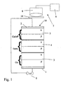
- Fig. 1 shows schematically the structure of a triple junction solar cell as a special Example of a multi junction solar cell.
- This consists of a vertical sequence of three solar cells 3, 4, 5, each having a pn junction in the vertical direction include.
- the lowermost solar cell 3 consists in the example of FIG. 1 of a Semiconductor layer of germanium, an indirect bandpass semiconductor, which for forming the pn junction, a lower p-doped region and has an upper n-doped region.
- the center solar cell 4 in Fig. 1 consists a layer of GaAs, a direct bandpass semiconductor, and also includes a p-doped and n-doped region for formation a vertical pn junction.
- the upper solar cell 5 is made of GalnP, as well a direct band-pass semiconductor, and also contains a p-doped one and an n-doped region for forming a vertical pn junction.
- the lower solar cell 3 may, for example, by a doped Ge wafers are to be gebilet.
- the thicknesses of the semiconductor layers of the solar cells 4 and 5 can be in the range of a few micrometers.
- doped semiconductor layers to form the pn junctions can between or adjacent to these layers even more doped or undoped Layers are provided to optimize the effect of pn junctions or additional electrical elements such as diodes between the layers train.
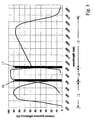
- the absorption behavior of the individual solar cells 3, 4, 5 of the triple junction solar cell is schematically in Fig. 3 based on the given effectiveness of the generation represented by charge carriers as a function of wavelength.
- the upper solar cell 5 absorbs electromagnetic radiation in a wavelength range 13 of 300 nm to 700 nm, the central solar cell 4 in a range 14 from 700 nm to 900 nm and the lower solar cell 3 in a range 15 of 900 nm to 1700 nm.
- the energy corresponds to the respective cutoff wavelength 16, 17 of the absorption spectra 13, 14 of the solar cells 4, 5 the respective minimum band gap between conduction band and valence band of the semiconductor, that is to say in the case of the solar cells 4, 5 of the energy difference for the direct band transition.
- the lower solar cell 3 is connected to an electrode 1, the upper solar cell 5 with a Etektrode 2.
- a voltage 6 is applied which is designed such that all three pn junctions, which are formed by the three solar cells 3, 4, 5, operated in the forward direction become.
- this voltage is in the range from a few volts.
- the amperage can be adjusted so that a sufficient Radiation behavior of the solar cell arrangement is given, a destruction the solar cell arrangement by excessive currents but excluded is.
- charge carriers (electrons and Holes) in the semiconductor layers of the solar cells 3, 4, 5 induced.
- the electrons of the conduction band can be due to in the semiconductor layers of the solar cells 4, 5 the present direct band transition radiant, so under transmission of photons, recombine with holes in the valence band.
- the energy the photons just corresponds to the band gap in the region of the direct band transition, So for the upper solar cell 5 a wavelength 16 of 700 nm (red Light) and for the central solar cell 4 a wavelength 17 of 900 nm (infrared).
- the lower solar cell in Fig. 1 does not emit radiation, as in germanium an indirect Band transition is present, so no radiative recombination of the charge carriers is possible.
- the radiation behavior along the surface 10 of the entire solar cell arrangement can now, for example, automatically by an image processing device 7 are recorded and analyzed.
- image processing device 7 are basically out of state known in the art and usually have an optical sensor 8 (for example a CCD camera) for detecting the radiation and a processing device 9 for signal processing and image recognition or image processing on.
- This device 7 is to be interpreted as having the desired Wavelengths 16, 17 can capture.
- per wavelength 16, 17 each to provide a device 7.
- Filtering out the device reaching the device 7 is ideally to provide a filter device 18, which in the case of Fig. 1 from a respective filter per wavelength 16, 17 can exist.
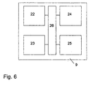
- Fig. 6 shows schematically as a block diagram the essential functionalities of a possible embodiment of the processing device 9 in detail.
- This shows a first image data storage area 22 for storing a radiation image a first semiconductor layer, a second image data storage area 23 for Storage of a radiation image of a second semiconductor layer, a first Program memory area 24 containing an image processing program, formed for the automatic examination of at least one of the radiation images abrupt, one-dimensionally extended intensity changes and for labeling the detected intensity changes as mechanical defects of the Semiconductor device and a second program memory area 25th comprising a program for analyzing at least one of the radiation images electrical effects of mechanical defects.
- the two programs can be carried out by a computer unit 26, which with the individual Memory areas 22 to 25 is connected by data technology.
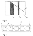
- FIG. 2 now schematically shows an image of the surface 10 of the solar cell arrangement from Fig. 1 with applied voltage in the forward direction.
- the surface 10 appear from the underneath through the radiated photons lying semiconductor layer of the solar cell 4 or 5 (depending on the selected filter 18) as bright areas.
- this in plan view of the surface 10 by abrupt intensity changes 11, 12, 19 detectable in the radiation behavior. For example, this indicates the one-dimensional intensity change 19 to a break in the corresponding one Semiconductor layer out, so on a mechanical defect.
- These abrupt Intensity changes 11, 12, 19 allow automatic detection very easily allow defects by common image processing systems. This can be off the radiation behavior of the solar cell arrangement, the optical in a simple manner can be analyzed directly, clearly and reproducibly for defects in the solar cell array are closed.
- Anomalous photon emission may be due to electrical result in inactive areas or by clouding. If it is are inactive areas, they may be due to mechanical defects to have.
- the method illustrated with reference to FIG. 4 can be mechanical Defects are detected and their effects on the electrical behavior of the Solar cell arrangement can be determined. It is from the total radiation by a suitable first filter 18, the wavelength 17 of the solar cell 4 in the infrared range filtered out and from the radiation image, the presence of mechanical Defects such as breaks are detected (see Fig. 4 b). Because all layers of the solar cells 4, 5 produced by epitaxial growth on the Ge wafer with the solar cell 3 can be concluded that appropriate mechanical Defects such as cracks are also present in the solar cells 3 and 5.
- the illustrated method has the advantage that even deep-lying defects and not just superficial defects, such as some of the procedures According to the state of the art.
- the defects can be classified by whether they have the pn junction in 0, 1 or 2 dimensions.
- 0-dimensional defects are punctiform Defects, e.g. to an increased photon emission to individual Lead points ("hot spots").
- 1-dimensional defects are in particular fractures 19, as shown in Fig. 2, which does not necessarily lead to electrical failure larger areas, but only in the immediate area of the fault line 19 disturb a pn junction. They are visually sharp at a sharp contrast to recognize.
- 2-dimensional defects 11, 12 are due to flat failure of a pn junction characterized (for example by damage to the electrical contact in the area of a break), at whose edges also a sharp contrast change occurs. It can even be deduced directly from the ratio of the areas of light and dark areas of the surface 10 to each other, the respective efficiency determine the respective solar cell 4, 5 and thus quantitatively a quality of the solar cell array determine.
- FIG. 5 shows a plurality of solar cell arrangements 20, for example a plurality of triple Junction Solar cell arrangements, which are combined into a string.
- the individual solar cell arrangements 20 via their electrodes 1, 2 connected in series.
- the solar cell assemblies 20 are on a common Carrier 21 applied. Now put a tension on this entire string which is n times the voltage in n solar cell assemblies 20, to turn on a solar cell array 20 in the forward direction, so The entire string of solar cells can be tested in one go.
Landscapes
- Health & Medical Sciences (AREA)
- Biochemistry (AREA)
- Physics & Mathematics (AREA)
- Life Sciences & Earth Sciences (AREA)
- Chemical & Material Sciences (AREA)
- Analytical Chemistry (AREA)
- General Health & Medical Sciences (AREA)
- General Physics & Mathematics (AREA)
- Immunology (AREA)
- Pathology (AREA)
- Nuclear Medicine, Radiotherapy & Molecular Imaging (AREA)
- Photovoltaic Devices (AREA)
- Testing Or Measuring Of Semiconductors Or The Like (AREA)
- Testing Of Individual Semiconductor Devices (AREA)
Description
- an zumindest einen pn-Übergang eines Halbleiter-Bauelements eine Spannung zum Betrieb des pn-Überganges in Durchlassrichtung angelegt wird, und
- das durch die angelegte Spannung erzeugte Strahlungsverhalten der Halbleiterschicht zumindest für Teilbereiche der Halbleiterschicht automatisch optisch erfasst und ausgewertet wird. Die spezielle Verwendung dieses Verfahrens im Rahmen der Erfindung betrifft eine Verwendung zur Detektion mechanischer Defekte des Halbleiter-Bauelements.
- eine Spannungsversorgung, die mit den Elektroden des Halbleiter-Bauelements verbindbar ist und zum Betrieb des pn-Überganges in Durchlassrichtung ausgelegt ist, und
- eine Einrichtung zur optischen Erfassung und Auswertung des durch die angelegte Spannung erzeugte Strahlungsverhalten der Halbleiterschicht zumindest für Teilbereiche der Halbleiterschicht.
- einen ersten Bilddaten-Speicherbereich zur Speicherung eines Strahlungsbildes einer ersten Halbleiterschicht
- einen zweiten Bilddaten-Speicherbereich zur Speicherung eines Strahlungsbildes einer zweiten Halbleiterschicht,
- einen ersten Programm-Speicherbereich enthaltend ein Bildverarbeitungsprogramm, ausgebildet zur automatischen Untersuchung mindestens eines der Strahlungsbilder auf abrupte, eindimensional ausgedehnte Intensitätsänderungen und zur Kennzeichnung der detektierten Intensitätsänderungen als mechanische Defekte des Halbleiter-Bauelements und
- einen zweiten Programm-Speicherbereich enthaltend ein Programm zur Analyse mindestens eines der Strahlungsbilder auf elektrische Auswirkungen der mechanischen Defekte.
- Fig. 1:
- Schematische Darstellung des optischen Tests einer Triple Junction Solarzellen-Anordnung,
- Fig. 2:
- Schematische Darstellung der Intensitätsverteilung entlang einer Halbleiterschicht mit Defekten,
- Fig. 3:
- Spektrale Emfpfindlichkeit einer Triple Juncion Solarzellen-Anordnung,
- Fig. 4:
- Schematische Darstellung der Intensitätsverteilung entlang zweier Solarzellen einer Triple Junction Solarzellen-Anordnung bei jeweils verschiedenen Wellenlängen
- Fig. 5:
- Schematische Darstellung mehrerer Solarzellen-Anordnung, zusammengefasst zu einem String
- Fig. 6:
- Schematische Darstellung einer Bildverarbeitungseinrichtüng
Claims (14)
- Verfahren zur Detektion von Defekten in einem Halbleiter-Bauelement (3, 4, 5, 20) mit zumindest einem pn-Übergang und zumindest einer Halbleiterschicht aus einem Halbleitermaterial mit direktem Bandübergang, wobei an den zumindest einen pn-Übergang eine Spannung zum Betrieb des pn-Überganges in Durchlassrichtung angelegt wird, und das durch die angelegte Spannung erzeugte Strahlungsverhalten der Halbleiterschicht zumindest für Teilbereiche der Halbleiterschicht optisch erfasst und ausgewertet wird, dadurch gekennzeichnet, dass das Strahlungsverhalten der Halbleiterschicht automatisch auf abrupte, eindimensional ausgedehnte Intensitätsänderungen (19) längs der Halbleiterschicht untersucht wird und detektierte Intensitätsänderungen (19) als mechanische Defekte des Halbleiter-Bauelements gekennzeichnet werden, und/oder
dass automatisch das Integral über die Strahlungsintensität zumindest eines ersten Teilbereichs einer ersten Halbleiterschicht bestimmt wird, anschließend das Integral über die Strahlungsintensität zumindest eines Vergleichsbereichs derselben Halbleiterschicht oder einer zweiten Halbleiterschicht bestimmt wird und aufgrund des Ergebnisses eines automatischen Vergleichs der beiden Integrale der erste Teilbereich als defekt oder als defektfrei gekennzeichnet wird. - Verfahren nach Anspruch 1, dadurch gekennzeichnet, dass eine indirekte Detektion mechanischer Defekte einer strahlungsinaktiven Schicht des Halbleiter-Bauelements (3) erfolgt, wobei das Strahlungsverhalten einer benachbarten strahlungsaktiven Halbleiterschicht automatisch auf abrupte, eindimensional ausgedehnte Intensitätsänderungen (19) längs der Halbleiterschicht untersucht wird und detektierte Intensitätsänderungen als mechanische Defekte der strahlungsinaktiven Schicht des Halbleiter-Bauelements (3) gekennzeichnet werden.
- Verfahren nach Anspruch 1 oder 2, dadurch gekennzeichnet, dass eine kombinierte Detektion von mechanischen Defekten und Erfassung der elektrischen Auswirkungen der mechanischen Defekte erfolgt, wobei eine Analyse des Strahlungsverhaltens des Bauelements (3, 4, 5, 20) in einem ersten Wellenlängenbereich (17) der Detektion mechanischer Defekte und eine Analyse des Strahlungsverhaltens des Bauelements (3, 4, 5, 20) in einem zweiten Wellenlängenbereich (16) der Erfassung der elektrischen Auswirkungen zu Grunde gelegt wird.
- Verfahren nach Anspruch 3, dadurch gekennzeichnet, dass das Strahlungsverhalten einer ersten Halbleiterschicht mit zumindest einem pn-Übergang zur Detektion mechanischer Defekte und das Strahlungsverhalten einer zweiten Halbleiterschicht mit zumindest einem pn-Übergang zur Erfassung der elektrischen Auswirkungen der mechanischen Defekte verwendet wird, wobei mittels einer Filteranordnung (18) jeweils diejenigen Wellenlängen (16, 17) aus dem Strahlungsspektrum herausgefiltert werden, deren Energie dem direkten Brandübergang der jeweilgen Halbleiterschicht entspricht.
- Verfahren nach einem der Ansprüche 1 bis 4, dadurch gekennzeichnet, dass eine Mehrzahl von n Halbleiter-Bauelementen (20) in einer Serienschaltung auf einem gemeinsamen Bauelemente-Träger (21) angeordnet wird und an die Gesamtheit der Halbleiter-Bauelemente (20) eine Spannung angelegt wird, die dem n-fachen der Spannung zum Betrieb eines Bauelementes (20) in Durchlassrichtung entspricht.
- Verwendung eines Verfahrens, bei demzur Detektion mechanischer Defekte des Halbleiter-Bauelements (3, 4, 5, 20), dadurch gekennzeichnet, dass das Strahlungsverhalten der Halbleiterschicht automatisch auf abrupte, eindimensional ausgedehnte Intensitätsänderungen(19) längs der Halbleiterschicht untersucht wird und detektierte Intensitätsänderungen als mechanische Defekte des Halbleiter-Bauelements (3, 4, 5, 20) gekennzeichnet werden, und/oderan zumindest einen pn-Übergang eines Halbleiter-Bauelements (3, 4, 5, 20) eine Spannung zum Betrieb des pn-Überganges in Durchlassrichtung angelegt wird, unddas durch die angelegte Spannung erzeugte Strahlungsverhalten der Halbleiterschicht zumindest für Teilbereiche der Halbleiterschicht automatisch optisch erfasst und ausgewertet wird,
dass automatisch das Integral über die Strahlungsintensität zumindest eines ersten Teilbereichs einer ersten Halbleiterschicht bestimmt wird, anschließend das Integral über die Strahlungsintensität zumindest eines Vergleichsbereichs derselben Halbleiterschicht oder einer zweiten Halbleiterschicht bestimmt wird und aufgrund des Ergebnisses eines automatischen Vergleichs der beiden Integrale der erste Teilbereich als defekt oder als defektfrei gekennzeichnet wird. - Verwendung nach Anspruch 6, dadurch gekennzeichnet, dass eine indirekte Detektion mechanischer Defekte einer strahlungsinaktiven Schicht des Halbleiter-Bauelements (3) erfolgt, wobei das Strahlungsverhalten einer benachbarten strahlungsaktiven Halbleiterschicht automatisch auf abrupte, eindimensional ausgedehnte Intensitätsänderungen (19) längs der Halbleiterschicht untersucht wird und detektierte Intensitätsänderungen als mechanische Defekte der strahlungsinaktiven Schicht des Halbleiter-Bauelements (3) gekennzeichnet werden.
- Verwendung nach einem der Ansprüche 6 oder 7, dadurch gekennzeichnet, dass eine kombinierte Detektion von mechanischen Defekten und Erfassung der elektrischen Auswirkungen der mechanischen Defekte erfolgt, wobei eine Analyse des Strahlungsverhaltens des Bauelements (3, 4, 5, 20) in einem ersten Wellenlängenbereich (17) der Detektion mechanischer Defekte und eine Analyse des Strahlungsverhaltens des Bauelements (3, 4, 5, 20) in einem zweiten Wellenlängenbereich (16) der Erfassung der elektrischen Auswirkungen zu Grunde gelegt wird.
- Verwendung nach Anspruch 8, dadurch gekennzeichnet, dass das Strahlungsverhalten einer ersten Halbleiterschicht mit zumindest einem pn-Übergang zur Detektion mechanischer Defekte und das Strahlungsverhalten einer zweiten Halbleiterschicht mit zumindest einem pn-Übergang zur Erfassung der elektrischen Auswirkungen der mechanischen Defekte verwendet wird, wobei mittels einer Filteranordnung (18) jeweils diejenigen Wellenlängen (16, 17) aus dem Strahlungsspektrum herausgefiltert werden, deren Energie dem direkten Bandübergang der jeweilgen Halbleiterschicht entspricht.
- Verwendung nach einem der Ansprüche 6 bis 9, dadurch gekennzeichnet, dass eine Mehrzahl von n Halbleiter-Bauelementen (20) in einer Serienschaltung auf einem gemeinsamen Bauelemente-Träger (21) angeordnet wird und an die Gesamtheit der Halbleiter-Bauelemente (20) eine Spannung angelegt wird, die dem n-fachen der Spannung zum Betrieb eines Bauelementes (20) in Durchlassrichtung entspricht.
- Verwendung nach einem der Ansprüche 6 bis 10 zur Detektion mechanischer Defekte von Solarzellen-Anordnungen (20).
- Anordnung zur Detektion mechanischer Defekte eines Halbleiter-Bauelements (3, 4, 5, 20), insbesondere von Solarzellen-Anordnungen (20), mit zumindest einem pn-Übergang und zumindest einer Halbleiterschicht aus einem Halbleitermaterial mit direktem Bandübergang und mindestens einer Elektrode (1 ), die mit dem p-leitenden Bereich des Halbleiter-Bauelements (3, 4, 5, 20) verbunden ist und mindestens einer Elektrode (2), die mit dem n-leitenden Bereich des Halbleiter-Bauelements (3, 4, 5, 20) verbunden ist, mit:gekennzeichnet durcheiner Spannungsversorgung (6), die mit den Elektroden (1, 2) des Halbleiter-Bauelements (3, 4, 5, 20) verbindbar ist und zum Betrieb des pn-Überganges in Durchlassrichtung ausgelegt ist,einer Einrichtung (7) zur optischen Erfassung und Auswertung des durch die angelegte Spannung erzeugte Strahlungsverhalten der Halbleiterschicht zumindest für Teilbereiche der Halbleiterschicht,einen ersten Bilddaten-Speicherbereich (22) zur Speicherung eines Strahlungsbildes einer ersten Halbleiterschicht,einen zweiten Bilddaten-Speicherbereich (23) zur Speicherung eines Strahlungsbildes einer zweiten Halbleiterschicht,einen ersten Programm-Speicherbereich (24) enthaltend ein Bildverarbeitungsprogramm, ausgebildet zur automatischen Untersuchung mindestens eines der Strahlungsbilder auf abrupte, eindimensional ausgedehnte Intensitätsänderungen (19) und zur Kennzeichnung der detektierten Intensitätsänderungen als mechanische Defekte des Halbleiter-Bauelements undeinen zweiten Programm-Speicherbereich (25) enthaltend ein Programm zur Analyse mindestens eines der Strahlungsbilder auf elektrische Auswirkungen der mechanischen Defekte.
- Anordnung nach Anspruch 12, gekennzeichnet durch eine Filteranordnung (18) zur Herausfilterung derjenigen Wellenlänge (16, 17) aus dem Strahlungsspektrum, deren Energie dem direkten Bandübergang der Halbleiterschicht entspricht.
- Anordnung nach Anspruch 12 zur Detektion mechanischer Defekte eines Halbleiter-Bauelements(3, 4, 5,20) mit mehreren pn-Übergängen und zumindest zwei Halbleiterschichten aus verschiedenen Halbleitermaterialien mit direktem Bandübergang, dadurch gekennzeichnet, dass jeweils eine Filteranordnung (18) pro Halbleiterschicht mit direktem Bandübergang vorgesehen ist zur Herausfilterung derjenigen Wellenlänge aus dem Strahlungsspektrum, deren Energie dem direkten Bandübergang der jeweiligen Halbleiterschicht entspricht.
Priority Applications (3)
| Application Number | Priority Date | Filing Date | Title |
|---|---|---|---|
| DE50202388T DE50202388D1 (de) | 2002-10-23 | 2002-10-23 | Verfahren und Anordnung zur optischen Detektion mechanischer Defekte in Halbleiter-Bauelementen, insbesondere in Solarzellen-Anordnungen |
| AT02023566T ATE290219T1 (de) | 2002-10-23 | 2002-10-23 | Verfahren und anordnung zur optischen detektion mechanischer defekte in halbleiter-bauelementen, insbesondere in solarzellen-anordnungen |
| EP02023566A EP1416288B1 (de) | 2002-10-23 | 2002-10-23 | Verfahren und Anordnung zur optischen Detektion mechanischer Defekte in Halbleiter-Bauelementen, insbesondere in Solarzellen-Anordnungen |
Applications Claiming Priority (1)
| Application Number | Priority Date | Filing Date | Title |
|---|---|---|---|
| EP02023566A EP1416288B1 (de) | 2002-10-23 | 2002-10-23 | Verfahren und Anordnung zur optischen Detektion mechanischer Defekte in Halbleiter-Bauelementen, insbesondere in Solarzellen-Anordnungen |
Publications (2)
| Publication Number | Publication Date |
|---|---|
| EP1416288A1 EP1416288A1 (de) | 2004-05-06 |
| EP1416288B1 true EP1416288B1 (de) | 2005-03-02 |
Family
ID=32087949
Family Applications (1)
| Application Number | Title | Priority Date | Filing Date |
|---|---|---|---|
| EP02023566A Expired - Lifetime EP1416288B1 (de) | 2002-10-23 | 2002-10-23 | Verfahren und Anordnung zur optischen Detektion mechanischer Defekte in Halbleiter-Bauelementen, insbesondere in Solarzellen-Anordnungen |
Country Status (3)
| Country | Link |
|---|---|
| EP (1) | EP1416288B1 (de) |
| AT (1) | ATE290219T1 (de) |
| DE (1) | DE50202388D1 (de) |
Cited By (1)
| Publication number | Priority date | Publication date | Assignee | Title |
|---|---|---|---|---|
| DE102007007140A1 (de) | 2007-02-09 | 2008-08-21 | Astrium Gmbh | Verfahren und Anordnung zur Detektion mechanischer Defekte eines Halbleiter-Bauelements, insbesondere einer Solarzelle oder Solarzellen-Anordnung |
Families Citing this family (11)
| Publication number | Priority date | Publication date | Assignee | Title |
|---|---|---|---|---|
| US7601941B2 (en) * | 2004-11-30 | 2009-10-13 | National University Corporation NARA Institute of Science and Technology | Method and apparatus for evaluating solar cell and use thereof |
| US7705978B2 (en) | 2006-02-06 | 2010-04-27 | Northrop Grumman Corporation | Method and apparatus for inspection of multi-junction solar cells |
| US7847237B2 (en) | 2006-05-02 | 2010-12-07 | National University Corporation Nara | Method and apparatus for testing and evaluating performance of a solar cell |
| CN103185854B (zh) | 2006-05-05 | 2015-07-01 | Bt成像股份有限公司 | 利用发光成像测试间接带隙半导体器件的方法和系统 |
| JP5243785B2 (ja) * | 2007-12-28 | 2013-07-24 | 日清紡ホールディングス株式会社 | 太陽電池検査装置及び太陽電池欠陥判定方法 |
| WO2010099964A2 (en) * | 2009-03-05 | 2010-09-10 | Oerlikon Solar Ag, Trübbach | Method and apparatus for measurement of ohmic shunts in thin film modules with the voc-ilit technique |
| CN101696942B (zh) * | 2009-10-16 | 2011-03-30 | 厦门大学 | 多结太阳能电池及各子电池交流电致发光测试方法和装置 |
| ES2712076T3 (es) | 2009-12-18 | 2019-05-09 | Isra Vision Graphikon Gmbh | Procedimiento y dispositivo para encontrar puntos defectuosos en elementos constructivos semiconductores |
| US8301409B2 (en) * | 2009-12-23 | 2012-10-30 | General Electric Company | Photon imaging system for detecting defects in photovoltaic devices, and method thereof |
| EP2378278B1 (de) * | 2010-04-19 | 2018-03-28 | Airbus Defence and Space GmbH | Verfahren zum Screening von Solarzellen mit mehreren Übergängen |
| CN108365051B (zh) * | 2018-02-05 | 2019-08-02 | 河北工业大学 | 一种太阳能电池片轨道去除的方法 |
Family Cites Families (2)
| Publication number | Priority date | Publication date | Assignee | Title |
|---|---|---|---|---|
| US5006717A (en) * | 1988-12-26 | 1991-04-09 | Matsushita Electric Industrial Co., Ltd. | Method of evaluating a semiconductor device and an apparatus for performing the same |
| US6225640B1 (en) * | 1999-05-19 | 2001-05-01 | Hughes Electronics Corporation | Method for electrical shunt detection and removal on semiconductors |
-
2002
- 2002-10-23 EP EP02023566A patent/EP1416288B1/de not_active Expired - Lifetime
- 2002-10-23 DE DE50202388T patent/DE50202388D1/de not_active Expired - Lifetime
- 2002-10-23 AT AT02023566T patent/ATE290219T1/de not_active IP Right Cessation
Cited By (3)
| Publication number | Priority date | Publication date | Assignee | Title |
|---|---|---|---|---|
| DE102007007140A1 (de) | 2007-02-09 | 2008-08-21 | Astrium Gmbh | Verfahren und Anordnung zur Detektion mechanischer Defekte eines Halbleiter-Bauelements, insbesondere einer Solarzelle oder Solarzellen-Anordnung |
| DE102007007140B4 (de) * | 2007-02-09 | 2009-01-29 | Astrium Gmbh | Verfahren und Anordnung zur Detektion mechanischer Defekte eines Halbleiter-Bauelements, insbesondere einer Solarzelle oder Solarzellen-Anordnung |
| EP3514523A1 (de) * | 2007-02-09 | 2019-07-24 | Airbus Defence and Space | Verfahren und anordnung zur detektion mechanischer defekte eines halbleiter-bauelements, insbesondere einer solarzelle oder solarzellen-anordnung |
Also Published As
| Publication number | Publication date |
|---|---|
| ATE290219T1 (de) | 2005-03-15 |
| DE50202388D1 (de) | 2005-04-07 |
| EP1416288A1 (de) | 2004-05-06 |
Similar Documents
| Publication | Publication Date | Title |
|---|---|---|
| DE112007001071B4 (de) | Verfahren und Vorrichtung zur Bewertung von Solarzellen und deren Verwendung | |
| EP2115435B1 (de) | Verfahren und anordnung zur detektion mechanischer defekte eines halbleiter-bauelements, insbesondere einer solarzelle oder solarzellen-anordnung | |
| EP2494339B2 (de) | Verfahren zur detektion von rissen in halbleitersubstraten | |
| EP1416288B1 (de) | Verfahren und Anordnung zur optischen Detektion mechanischer Defekte in Halbleiter-Bauelementen, insbesondere in Solarzellen-Anordnungen | |
| EP2883042B1 (de) | Verfahren und vorrichtung zum prüfen von photovoltaikmodulen | |
| EP2245473B1 (de) | Messverfahren und vorrichtung zur charakterisierung eines halbleiterbauelements | |
| DE112012002619T5 (de) | Verfahren und Vorrichtung zur Inspektion von lichtemittierenden Halbleiterelementen mittels Photolumineszenz-Abbildung | |
| WO2013167428A1 (de) | Verfahren und vorrichtung zur elektrolumineszenz-inspektion und/oder fotolumineszenz-inspektion | |
| EP1758178A2 (de) | Verfahren und Vorrichtung zur Ermittlung von Produktionsfehlern in einem Halbleiterbauelement | |
| DE10016996C1 (de) | Testanordnung zur Funktionsprüfung eines Halbleiterchips | |
| DE102009053504B3 (de) | Verfahren und Vorrichtung zur Bestimmung der Quanteneffizienz einer Solarzelle | |
| EP4014027B1 (de) | Verfahren und vorrichtung zur analyse einer mehrfachsolarzelle mit zumindest zwei sub-solarzellen mittels lumineszenzstrahlung | |
| DE102016114459A1 (de) | Verfahren und Vorrichtung zur Vermessung einer Vielzahl an Halbleiterchips in einem Waferverbund | |
| EP2336752A1 (de) | Verfahren un Vorrichtung zum Auffinden von Fehlstellen in Halbleiterbauelementen | |
| DE102020119323B3 (de) | Verfahren zur Analyse einer Vielzahl von optischen Halbleiterbauelementen | |
| EP0333017B1 (de) | Verfahren zur optischen Konzentrationsmessung | |
| DE102006028056B4 (de) | Verfahren zum Prüfen von Solarzellenmodulen und Prüfvorrichtung | |
| DE102009003544B4 (de) | Verfahren zur Überprüfung von Solarzellenoberflächen | |
| DE112016006757B4 (de) | Verfahren zur Überwachung eines Laserstrukturierungsvorgangs zur Bildung von Isolationsgräben in einem Solarmodul | |
| DE10248504B4 (de) | Zerstörungsfreies Analyseverfahren zur Güteermittlung einer Solarzelle auf Chalkopyritbasis | |
| WO2010142270A1 (de) | Zerstörungsfreies analyseverfahren zur güteermittlung einer dünnschichtsolarzelle mittels photolumineszenzspektroskopie | |
| DE10036177C2 (de) | Verfahren zum Testen von Halbleitereinrichtungen | |
| DE19915051C2 (de) | Verfahren und Vorrichtung zur ortsaufgelösten Charakterisierung elektronischer Eigenschaften von Halbleitermaterialien | |
| DE19636229A1 (de) | Verfahren und Vorrichtung zur Bestimmung der Degradationsprozesse in Halbleiterlasern | |
| WO2016162398A1 (de) | Vorrichtung zum detektieren von elektronischen defekten an halbleiterwafern auf silizium-basis |
Legal Events
| Date | Code | Title | Description |
|---|---|---|---|
| PUAI | Public reference made under article 153(3) epc to a published international application that has entered the european phase |
Free format text: ORIGINAL CODE: 0009012 |
|
| 17P | Request for examination filed |
Effective date: 20021023 |
|
| AK | Designated contracting states |
Kind code of ref document: A1 Designated state(s): AT BE BG CH CY CZ DE DK EE ES FI FR GB GR IE IT LI LU MC NL PT SE SK TR |
|
| AX | Request for extension of the european patent |
Extension state: AL LT LV MK RO SI |
|
| 17Q | First examination report despatched |
Effective date: 20040503 |
|
| GRAP | Despatch of communication of intention to grant a patent |
Free format text: ORIGINAL CODE: EPIDOSNIGR1 |
|
| GRAS | Grant fee paid |
Free format text: ORIGINAL CODE: EPIDOSNIGR3 |
|
| GRAA | (expected) grant |
Free format text: ORIGINAL CODE: 0009210 |
|
| AKX | Designation fees paid |
Designated state(s): AT BE BG CH CY CZ DE DK EE ES FI FR GB GR IE IT LI LU MC NL PT SE SK TR |
|
| AK | Designated contracting states |
Kind code of ref document: B1 Designated state(s): AT BE BG CH CY CZ DE DK EE ES FI FR GB GR IE IT LI LU MC NL PT SE SK TR |
|
| PG25 | Lapsed in a contracting state [announced via postgrant information from national office to epo] |
Ref country code: TR Free format text: LAPSE BECAUSE OF FAILURE TO SUBMIT A TRANSLATION OF THE DESCRIPTION OR TO PAY THE FEE WITHIN THE PRESCRIBED TIME-LIMIT Effective date: 20050302 Ref country code: FI Free format text: LAPSE BECAUSE OF FAILURE TO SUBMIT A TRANSLATION OF THE DESCRIPTION OR TO PAY THE FEE WITHIN THE PRESCRIBED TIME-LIMIT Effective date: 20050302 Ref country code: IE Free format text: LAPSE BECAUSE OF FAILURE TO SUBMIT A TRANSLATION OF THE DESCRIPTION OR TO PAY THE FEE WITHIN THE PRESCRIBED TIME-LIMIT Effective date: 20050302 Ref country code: GB Free format text: LAPSE BECAUSE OF FAILURE TO SUBMIT A TRANSLATION OF THE DESCRIPTION OR TO PAY THE FEE WITHIN THE PRESCRIBED TIME-LIMIT Effective date: 20050302 Ref country code: EE Free format text: LAPSE BECAUSE OF FAILURE TO SUBMIT A TRANSLATION OF THE DESCRIPTION OR TO PAY THE FEE WITHIN THE PRESCRIBED TIME-LIMIT Effective date: 20050302 Ref country code: SK Free format text: LAPSE BECAUSE OF FAILURE TO SUBMIT A TRANSLATION OF THE DESCRIPTION OR TO PAY THE FEE WITHIN THE PRESCRIBED TIME-LIMIT Effective date: 20050302 Ref country code: CZ Free format text: LAPSE BECAUSE OF FAILURE TO SUBMIT A TRANSLATION OF THE DESCRIPTION OR TO PAY THE FEE WITHIN THE PRESCRIBED TIME-LIMIT Effective date: 20050302 |
|
| REG | Reference to a national code |
Ref country code: GB Ref legal event code: FG4D Free format text: NOT ENGLISH |
|
| REG | Reference to a national code |
Ref country code: CH Ref legal event code: EP |
|
| REG | Reference to a national code |
Ref country code: IE Ref legal event code: FG4D Free format text: GERMAN |
|
| REF | Corresponds to: |
Ref document number: 50202388 Country of ref document: DE Date of ref document: 20050407 Kind code of ref document: P |
|
| PG25 | Lapsed in a contracting state [announced via postgrant information from national office to epo] |
Ref country code: GR Free format text: LAPSE BECAUSE OF FAILURE TO SUBMIT A TRANSLATION OF THE DESCRIPTION OR TO PAY THE FEE WITHIN THE PRESCRIBED TIME-LIMIT Effective date: 20050602 Ref country code: DK Free format text: LAPSE BECAUSE OF FAILURE TO SUBMIT A TRANSLATION OF THE DESCRIPTION OR TO PAY THE FEE WITHIN THE PRESCRIBED TIME-LIMIT Effective date: 20050602 Ref country code: BG Free format text: LAPSE BECAUSE OF FAILURE TO SUBMIT A TRANSLATION OF THE DESCRIPTION OR TO PAY THE FEE WITHIN THE PRESCRIBED TIME-LIMIT Effective date: 20050602 |
|
| PG25 | Lapsed in a contracting state [announced via postgrant information from national office to epo] |
Ref country code: ES Free format text: LAPSE BECAUSE OF FAILURE TO SUBMIT A TRANSLATION OF THE DESCRIPTION OR TO PAY THE FEE WITHIN THE PRESCRIBED TIME-LIMIT Effective date: 20050613 |
|
| PG25 | Lapsed in a contracting state [announced via postgrant information from national office to epo] |
Ref country code: PT Free format text: LAPSE BECAUSE OF FAILURE TO SUBMIT A TRANSLATION OF THE DESCRIPTION OR TO PAY THE FEE WITHIN THE PRESCRIBED TIME-LIMIT Effective date: 20050907 |
|
| GBV | Gb: ep patent (uk) treated as always having been void in accordance with gb section 77(7)/1977 [no translation filed] |
Effective date: 20050302 |
|
| REG | Reference to a national code |
Ref country code: IE Ref legal event code: FD4D |
|
| PG25 | Lapsed in a contracting state [announced via postgrant information from national office to epo] |
Ref country code: CY Free format text: LAPSE BECAUSE OF FAILURE TO SUBMIT A TRANSLATION OF THE DESCRIPTION OR TO PAY THE FEE WITHIN THE PRESCRIBED TIME-LIMIT Effective date: 20051023 Ref country code: AT Free format text: LAPSE BECAUSE OF NON-PAYMENT OF DUE FEES Effective date: 20051023 |
|
| PG25 | Lapsed in a contracting state [announced via postgrant information from national office to epo] |
Ref country code: BE Free format text: LAPSE BECAUSE OF NON-PAYMENT OF DUE FEES Effective date: 20051031 Ref country code: LU Free format text: LAPSE BECAUSE OF NON-PAYMENT OF DUE FEES Effective date: 20051031 Ref country code: MC Free format text: LAPSE BECAUSE OF NON-PAYMENT OF DUE FEES Effective date: 20051031 |
|
| PLBE | No opposition filed within time limit |
Free format text: ORIGINAL CODE: 0009261 |
|
| STAA | Information on the status of an ep patent application or granted ep patent |
Free format text: STATUS: NO OPPOSITION FILED WITHIN TIME LIMIT |
|
| 26N | No opposition filed |
Effective date: 20051205 |
|
| ET | Fr: translation filed | ||
| PG25 | Lapsed in a contracting state [announced via postgrant information from national office to epo] |
Ref country code: CH Free format text: LAPSE BECAUSE OF NON-PAYMENT OF DUE FEES Effective date: 20061031 Ref country code: LI Free format text: LAPSE BECAUSE OF NON-PAYMENT OF DUE FEES Effective date: 20061031 |
|
| REG | Reference to a national code |
Ref country code: CH Ref legal event code: PL |
|
| BERE | Be: lapsed |
Owner name: EADS ASTRIUM G.M.B.H. Effective date: 20051031 |
|
| PG25 | Lapsed in a contracting state [announced via postgrant information from national office to epo] |
Ref country code: SE Free format text: LAPSE BECAUSE OF FAILURE TO SUBMIT A TRANSLATION OF THE DESCRIPTION OR TO PAY THE FEE WITHIN THE PRESCRIBED TIME-LIMIT Effective date: 20050602 |
|
| REG | Reference to a national code |
Ref country code: FR Ref legal event code: PLFP Year of fee payment: 14 |
|
| REG | Reference to a national code |
Ref country code: FR Ref legal event code: PLFP Year of fee payment: 15 |
|
| REG | Reference to a national code |
Ref country code: FR Ref legal event code: PLFP Year of fee payment: 16 |
|
| REG | Reference to a national code |
Ref country code: DE Ref legal event code: R081 Ref document number: 50202388 Country of ref document: DE Owner name: AIRBUS DEFENCE AND SPACE GMBH, DE Free format text: FORMER OWNER: EADS ASTRIUM GMBH, 81667 MUENCHEN, DE |
|
| REG | Reference to a national code |
Ref country code: NL Ref legal event code: HC Owner name: AIRBUS DS GMBH; DE Free format text: DETAILS ASSIGNMENT: CHANGE OF OWNER(S), CHANGE OF OWNER(S) NAME; FORMER OWNER NAME: EADS ASTRIUM GMBH Effective date: 20180220 Ref country code: NL Ref legal event code: PD Owner name: AIRBUS DEFENCE AND SPACE GMBH; DE Free format text: DETAILS ASSIGNMENT: CHANGE OF OWNER(S), MERGE; FORMER OWNER NAME: AIRBUS DS GMBH Effective date: 20180220 |
|
| REG | Reference to a national code |
Ref country code: FR Ref legal event code: CA Effective date: 20180515 Ref country code: FR Ref legal event code: CD Owner name: ASTRIUM GMBH, DE Effective date: 20180515 |
|
| REG | Reference to a national code |
Ref country code: FR Ref legal event code: CD Owner name: AIRBUS DS GMBH, DE Effective date: 20180718 |
|
| REG | Reference to a national code |
Ref country code: FR Ref legal event code: PLFP Year of fee payment: 17 |
|
| PGFP | Annual fee paid to national office [announced via postgrant information from national office to epo] |
Ref country code: NL Payment date: 20211020 Year of fee payment: 20 |
|
| PGFP | Annual fee paid to national office [announced via postgrant information from national office to epo] |
Ref country code: DE Payment date: 20211020 Year of fee payment: 20 |
|
| PGFP | Annual fee paid to national office [announced via postgrant information from national office to epo] |
Ref country code: IT Payment date: 20211028 Year of fee payment: 20 Ref country code: FR Payment date: 20211021 Year of fee payment: 20 |
|
| REG | Reference to a national code |
Ref country code: DE Ref legal event code: R071 Ref document number: 50202388 Country of ref document: DE |
|
| REG | Reference to a national code |
Ref country code: NL Ref legal event code: MK Effective date: 20221022 |