EP1434382B2 - Appareil de transfert de donnees en serie - Google Patents
Appareil de transfert de donnees en serie Download PDFInfo
- Publication number
- EP1434382B2 EP1434382B2 EP01972652.0A EP01972652A EP1434382B2 EP 1434382 B2 EP1434382 B2 EP 1434382B2 EP 01972652 A EP01972652 A EP 01972652A EP 1434382 B2 EP1434382 B2 EP 1434382B2
- Authority
- EP
- European Patent Office
- Prior art keywords
- serial data
- receiving
- data
- start signal
- signal
- Prior art date
- Legal status (The legal status is an assumption and is not a legal conclusion. Google has not performed a legal analysis and makes no representation as to the accuracy of the status listed.)
- Expired - Lifetime
Links
Images


Classifications
-
- H—ELECTRICITY
- H04—ELECTRIC COMMUNICATION TECHNIQUE
- H04L—TRANSMISSION OF DIGITAL INFORMATION, e.g. TELEGRAPHIC COMMUNICATION
- H04L7/00—Arrangements for synchronising receiver with transmitter
- H04L7/04—Speed or phase control by synchronisation signals
- H04L7/10—Arrangements for initial synchronisation
-
- H—ELECTRICITY
- H04—ELECTRIC COMMUNICATION TECHNIQUE
- H04J—MULTIPLEX COMMUNICATION
- H04J3/00—Time-division multiplex systems
- H04J3/24—Time-division multiplex systems in which the allocation is indicated by an address the different channels being transmitted sequentially
-
- H—ELECTRICITY
- H04—ELECTRIC COMMUNICATION TECHNIQUE
- H04J—MULTIPLEX COMMUNICATION
- H04J7/00—Multiplex systems in which the amplitudes or durations of the signals in individual channels are characteristic of those channels
-
- H—ELECTRICITY
- H04—ELECTRIC COMMUNICATION TECHNIQUE
- H04L—TRANSMISSION OF DIGITAL INFORMATION, e.g. TELEGRAPHIC COMMUNICATION
- H04L7/00—Arrangements for synchronising receiver with transmitter
- H04L7/04—Speed or phase control by synchronisation signals
- H04L7/041—Speed or phase control by synchronisation signals using special codes as synchronising signal
- H04L7/046—Speed or phase control by synchronisation signals using special codes as synchronising signal using a dotting sequence
-
- H—ELECTRICITY
- H04—ELECTRIC COMMUNICATION TECHNIQUE
- H04L—TRANSMISSION OF DIGITAL INFORMATION, e.g. TELEGRAPHIC COMMUNICATION
- H04L7/00—Arrangements for synchronising receiver with transmitter
- H04L7/04—Speed or phase control by synchronisation signals
- H04L7/06—Speed or phase control by synchronisation signals the synchronisation signals differing from the information signals in amplitude, polarity or frequency or length
Definitions
- the present invention relates to a serial data transferring apparatus, which requires synchronization in data transfer to be established between the receiving side and the transmitting side.
- the inexpensive sensor device is mainly employed in the signal transfer using an analog voltage, and this type of signal transfer has limitations in transfer distance and transfer accuracy.
- the disclosed start-stop synchronization data transfer method requires neither the expensive quartz oscillator nor the PLL.
- EP 1014273A2 discloses a method of start/stop synchronous data transmission. It allows stabile start/ stop synchronous communication with a clock signal generated by an oscillator which has a relatively low level of oscillation frequency accuracy.
- the transmission is carried out between a master station having a high accuracy oscillating circuit adopted to a baud rate imaging transmission line characteristics and at least one slave station having a low accuracy oscillating circuit.
- the master station sends a predetermined dummy message at a predetermined period.
- the slave station counts clock pulses from the low accuracy oscillating circuit for a time interval between edges of a first bit frame of the dummy message.
- a baud rate clock signal is generated from the count of clock pulses according to a predetermined algorithm for start/ stop synchronous communication.
- the start-stop synchronization data transfer method requires a CR oscillator oscillating at frequency several hundreds times as high as a transfer clock of the data, and a digital circuit, e.g., a counter, which operates at the oscillation frequency of the CR oscillator and detects the transfer clock to establish the synchronization.
- a digital circuit e.g., a counter
- the transfer clock is limited by the highest oscillation frequency of the CR oscillator and the highest operation frequency of the digital circuit. This has invited a limitation in increasing the transfer clock frequency beyond such a limit.
- An object of the present invention is to provide a serial data transferring apparatus, which is inexpensive and can reduce noise.
- the present invention is constituted as follows:
- Fig. 1 shows a data communication sequence in a serial data transferring apparatus according to the first embodiment of the present invention
- Fig. 2 shows a schematic system configuration for the serial data transferring apparatus according to the first embodiment.
- Fig. 3 shows an internal configuration of a master unit and a slave unit in the serial data transferring apparatus according to the first embodiment of the present invention
- Fig. 4 shows a control sequence of the slave unit in the serial data according to the first embodiment of the present invention.
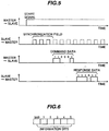
- Fig. 5 is a timing chart of transfer data in the first embodiment of the present invention
- Fig. 6 shows a bit configuration of command data and response data in the first embodiment of the present invention.
- a master unit 1 first sends a start signal to a slave unit 2.
- the slave unit 2 sends, to the master unit 1, a synchronization field that is a data train (pulse signal) indicative of a transfer clock with which the slave unit 2 is able to perform transferring and receiving operations.
- the master unit 1 sends, to the slave unit 2, command data in accordance with the transfer clock indicated by the synchronization field sent from the slave unit 2.
- the slave unit 2 sends, to the master unit 1, response data in accordance with the transfer clock indicated by the synchronization field.
- the master unit 1 establishes the synchronization for the data transfer, while the slave unit 2 is free from a burden of establishing the synchronization for the data transfer.
- master unit is used herein for the reason that the master unit 1 serves as a manager (master) for sending the start signal to the slave unit 2 and starting communication with respect to the slave unit 2.
- master unit the first embodiment of the present invention is constructed such that the master unit 1 generating the start signal and requesting communication performs serial communication in match with the operation clock of the slave unit 2 having no precise clock.
- serial data transferring apparatus By employing the serial data transferring apparatus according to the first embodiment of the present invention, as shown in Fig. 2 , one-to-one communication can be realized between a master unit 3 and slave units 4, 5, 6, 7, 8 and 9 each of which is connected to the master unit 3 by a single line.
- the master unit 3 and the slave units 4, 5, 6, 7, 8 and 9 are each provided with an open-drain or open-collector output driver for realizing two-way communication therebetween.
- the master unit 3 serves as a controller for collecting information from a plurality of slave units 4, 5 and 6, which are sensors, and controlling a plurality of slave units 7, 8 and 9, which are actuators.
- the master unit 3 solely takes a burden of establishing the synchronization for the data transfer, while the slave units 4, 5, 6, 7, 8 and 9 are free from the burden of establishing the synchronization for the data transfer.
- the construction of each of the slave units 4, 5, 6, 7, 8 and 9 can be simplified.
- slave units 4, 5, 6, 7, 8 and 9 in the form of sensors and actuators, which are constructed of primarily analog circuits, can be inexpensively incorporated in an apparatus for serially transferring digital signals.
- the synchronization for the data transfer is established only on the side of the master unit 3 instead of establishing the synchronization for the data transfer on the side of each of the slave units 4, 5, 6, 7, 8 and 9 as practiced in the above-mentioned prior art, the number of circuits required in an overall system for establishing the synchronization for the data transfer can be reduced and the serial data transfer can be realized without considerably increasing the circuit scale as a whole of the system.
- the slave units 4, 5, 6, 7, 8 and 9 are each required to include a digital circuit, e.g., a counter, for establishing the synchronization with an oscillator that oscillates signals at frequency several hundreds times as high as the data transfer rate.
- a digital circuit e.g., a counter
- the high-frequency oscillator and the digital circuit operating at the high frequency become serious noise sources in, e.g., a sensor handling a minute signal.
- the serial transfer can be performed in accordance with even a maximum one among clocks of the slave units 4, 5, 6, 7, 8 and 9, and hence the communication rate in the overall system can be increased.
- a microcomputer is used as the controller in many cases because absolute time management is required for the data transfer and a large amount of arithmetic processing is needed.
- An apparatus utilizing a microcomputer for that purpose includes a high-frequency quartz oscillator for operating the microcomputer and many high-frequency digital circuits in most cases.
- the master unit 1 in the serial data transferring apparatus comprises a microcomputer 10 for collecting information from the slave units serving as sensors and controlling actuators, a quartz oscillator 11 for generating a basic clock signal for operating the microcomputer 10, a start signal generator 15 for generating a start signal, a clock detection circuit 12 for detecting a transfer clock from a synchronization field, a transmitting circuit 14 for sending command data, a receiving circuit 13 for receiving response data, a pull-up resistor 16 for pulling up a signal line, transistors 17, 18 for driving the signal line, and a selector 19 for selectively changing over connection to the slave units.
- a microcomputer 10 for collecting information from the slave units serving as sensors and controlling actuators
- a quartz oscillator 11 for generating a basic clock signal for operating the microcomputer 10
- a start signal generator 15 for generating a start signal
- a clock detection circuit 12 for detecting a transfer clock from a synchronization field
- a transmitting circuit 14 for sending command data
- a receiving circuit 13 for receiving
- the start signal generator 15, the clock detection circuit 12, the transmitting circuit 14, and the receiving circuit 13 are controlled with the operation of the microcomputer 10.
- the slave unit 2 in the serial data transferring apparatus comprises a pull-up resistor 20 for pulling up a signal line, a transistor 21 for driving the signal line, a shift register 22 for executing serial/parallel conversion of the command data and the response data, an AND gate 23 for controlling an input and an output of the slave unit 2, a control circuit 24 for detecting the start signal, making an input/output to and from the shift register 22, and applying a signal to the AND gate 23, and a CR oscillator 25 for generating a clock signal to operate the control circuit 24 and the shift register 22.
- command data and the response data are each in the form of a data train having 6 bits as information bits, as shown in Fig. 6 .
- step 100 the control circuit 24 of the slave unit 2 first outputs a low-level signal to the AND gate 23, thereby turning off the transistor 21. Then, the slave unit 2 waits in step 101 until, as shown in Fig. 5 , the master unit 1 sends the start signal and the signal line takes a high level.
- the master unit 1 selects the slave unit 2 by the selector 19 and outputs the start signal from the start signal generator 15 (turns the signal line to a high level).
- step 102 Upon receiving the start signal, the slave unit 2 proceeds to step 102 in which the control circuit 24 outputs a high-level signal to the AND gate 23. Then, in step 103, a binary number of 010101 is written in the shift register 22.
- step 104 the shift register 22 waits for 6 clocks.
- step 105 the control circuit 24 outputs a low-level signal to the AND gate 23.
- the shift register 22 By causing the shift register 22 to always perform the shift operation in accordance with a clock signal from the CR oscillator 25, the data 010101 written in the shift register 22 is outputted to the signal line through the AND gate 23 and the transistor 21 so that the data 101010 is outputted to the signal line.
- This data serves as data indicating 1/2 of the transfer clock of the slave unit 2.
- the data indicating 1/2 of the transfer clock is called a synchronization field.
- the master unit 1 detects the transfer clock signal from the synchronization field by the clock detector 12 and sends the command data from the transmitting circuit 14.
- the command data is outputted in phase with the signal of 101010 in the synchronization field.
- the command data can be accurately transferred to the shift register 22 just by causing the shift register 22 of the slave unit 2 to perform the shift operation in accordance with the output clock of the CR oscillator 25.
- the slave unit 2 can read the command data just by waiting for 6 clocks in step 106 and then reading the shift register 25 in step 107.
- the slave unit 2 interprets the read command data in step 108, outputs a high-level signal to the AND gate 23 in step 109, and writes the response data in the shift register 22 in step 110.
- the response data written in the shift register 22 is hence outputted to the signal line through the AND gate 23 and the transistor 21.
- the master unit 1 reads the response data, which has been outputted to the signal line, by the receiving circuit 13, thereby completing the communication with respect to the slave unit 2.
- the slave unit 2 can be constructed of a very simple structure.
- the transmitting and receiving operations can be realized at a high rate.
- the oscillation frequency of the CR oscillator 25 may be equal to the frequency of the transfer clock, and the oscillation frequency several hundred times as high as the transfer clock is no longer required. Hence, there occurs no problem of noise, which is otherwise caused with the provision of a high-frequency oscillator.
- Fig. 7 is a timing chart of signals in the modification of the first embodiment. As seen from comparison with the embodiment shown in Fig. 5 wherein no substantial phase difference exists between the command data and the synchronization field, the modification shown in Fig. 7 differs from the embodiment shown in Fig. 5 in that the command data is delayed in phase by a 1/4-clock cycle relative to the synchronization field in the modification shown in Fig. 7 .
- the rising of the command data is delayed in phase by a 1/4-clock cycle relative to the synchronization field so that the hold time and the setup time are reliably secured.
- the delay in phase is not limited to the 1/4-clock cycle, and it may be set to any suitable predetermined value.
- Fig. 8 is an illustration showing a bit configuration of the command data and the response data used in the modification of the first embodiment.
- the bit configuration of the command data and the response data used in the serial data transferring apparatus is set to include a start bit as shown in Fig. 8 .
- start bit With the presence of the start bit, start-stop synchronization can be realized and therefore phase matching is facilitated.
- Fig. 9 is a diagram for explaining a communication sequence in still another modification of the first embodiment.
- the response data is not sent from the slave unit 2.
- This modification is adapted for the case of the slave unit 2 being an actuator or the like because, in such a case, the communication just requires outputting from the master unit 1 to the slave unit 2 and there is no necessity of sending a response.
- FIG. 10 Still another modification of the serial data transferring apparatus according to the first embodiment of the present invention will now be described with reference to Fig. 10 .
- the modification of Fig. 10 is shown as a diagram for explaining a communication sequence in the serial data transferring apparatus according to the first embodiment.
- the command data is not sent from the master unit 1.
- This modification is adapted for the case of the slave unit 2 being a sensor or the like because, in such a case, the communication just requires outputting of a measured result from the slave unit 2 to the master unit 1 and there is no necessity of receiving the command data.
- the command data is of course required.
- the command data is effective in changing over the measuring points or the measured physical quantities from one to another, or making a shift to a diagnosis mode.
- a serial data transferring apparatus according to a second embodiment of the present invention will be described below with reference to Figs. 11 and 12 .
- Fig. 11 shows a general system configuration of the serial data transferring apparatus according to the second embodiment of the present invention
- Fig. 12 is a timing chart of signals in the serial data transferring apparatus according to the second embodiment of the present invention.
- the system configuration of the serial data transferring apparatus is designed as a one-to-multiple communication system in which one signal line extended from a master unit 26 is connected to slave units 27, 28 and 29; namely one master unit 26 is communicated with a plurality of slave units.
- a communication system As shown in Fig. 12 , as shown in Fig. 12 , information representing an address of each slave unit (e.g., an address 2 of the slave unit 27, an address 3 of the slave unit 28, and an address 4 of the slave unit 29) is superimposed, as the number of pulses, on the start signal from the master unit 26.
- an address of each slave unit e.g., an address 2 of the slave unit 27, an address 3 of the slave unit 28, and an address 4 of the slave unit 29
- which one of the slave units 27, 28 and 29 has been selected can be identified by monitoring the signal line with two comparators having thresholds different from each other, detecting the start signal with the comparator having a first threshold, detecting pulses in the signal indicative of the address with the comparator having a second threshold, and counting the number of detected pulses.
- the slave unit having the address 4 i.e., the slave unit 29, is selected.
- the selected slave unit replies the synchronization field, receives the command data, and replies the response data.
- the second embodiment of the present invention can also provide similar advantages to those obtainable with the first embodiment.
- FIG. 13 shows a waveform of the start signal used in the serial data transferring apparatus according to the third embodiment of the present invention.
- the start signal used in the above-described second embodiment is modified as shown in Fig. 13 . More specifically, the start signal is made up of two blanks (each meaning a state where a signal is absent for a certain period), and pulses indicative of the address of the slave unit are superimposed between the two blanks.
- start signal formed as shown in Fig. 13 can also provide similar advantages to those obtainable with the first embodiment.
- FIG. 14 is a diagram for explaining a production line of sensor devices each including a serial data transferring apparatus according to a fourth embodiment of the present invention
- Fig. 15 is a block diagram of the sensor device including the serial data transferring apparatus according to the fourth embodiment
- Fig. 16 is a timing chart of signals in the sensor device according to the fourth embodiment.
- sensor devices 31, 32, 33, 34 and 35 are transported to flow successively along the production line from the left to the right, as viewed in Fig. 14 , relative to a check/adjustment device 30.
- the sensor device 33 is connected to the check/adjustment device 30.
- the serial data transferring apparatus is incorporated in each of the sensor devices 31, 32, 33, 34 and 35.
- the check/adjustment device 30 By connecting the check/adjustment device 30 to each of the sensor devices 31, 32, 33, 34 and 35 in turn, it is possible to write data, for example, in an internal monitor of the sensor device or an EPROM therein for storing adjustment information through one signal line by utilizing the incorporated communication apparatus.
- the use of only one signal line enables a signal terminal to be additionally provided in a connector or the like. Even after complete assembly of the sensor device, therefore, data can be written in the internal monitor of the sensor device or the EPROM therein for storing adjustment information.
- serial data transferring apparatus can satisfy those two demands.
- the sensor device including the fourth embodiment of the present invention comprises a sensing element 41 in which a physical variable changes depending on a measured quantity, a detection circuit 40 for converting a change of the physical variable in the sensing element 41 into an electrical signal, an adjustment circuit 39 for adjusting an output of the detection circuit 40 to a predetermined characteristic, an analog voltage output circuit 38 for outputting, as an analog voltage, an output of the adjustment circuit 39 to the exterior, a communication circuit 37 for executing communication with respect to the exterior, a selector 42 for changing over an output signal between the analog voltage outputted from the analog voltage output circuit 38 and a communication signal connected to the communication circuit, an EPROM 39 for storing adjustment information based on which the adjustment circuit 39 adjusts the characteristic, and a connector 43 for mechanically fixing signal terminals for a control signal and the output signal.
- the selector 42 is controlled in accordance with a control signal so that the output terminal is selectively changed over between the state of outputting the analog voltage and the state of performing communication.
- the analog voltage output circuit 38 is connected to the output signal and the analog voltage corresponding to a value measured by the sensing element 41 is outputted.
- the control signal is at 12 V
- the output signal is connected to the communication circuit 37 so as to allow communication from the exterior.
- this voltage can also be utilized as a high voltage required for writing data in the PROM 36, and hence a boosting circuit is omitted which must be otherwise incorporated in the sensor circuit. Also, by setting a threshold for the control signal to a relatively high value, a malfunction is harder to occur even when noise is imposed on the control signal.
- control signal is employed as the start signal indicative of the start of communication
- the circuit configuration of the communication circuit is simplified. The communication is performed by successively transferring, as the output signal, the synchronization field, the command data, and the response data in a similar manner to that described above.
- Fig. 17 is a timing chart of signals in a modification of the sensor device including the fourth embodiment.
- a pulse signal is supplied as the control signal and is also employed as the start signal.
- the communication is realized by successively transferring, as the output signal, the command data and the response data in sync with pulses of the control signal.
- the embodiments described above are constructed such that the master unit 1 transmits the start signal to the slave unit 2 and, in response to the start signal, the slave unit 2 transmits the synchronization field to the master unit 1.
- the slave unit 2 transmits both the start signal and the synchronization field to the master unit 1 and, in response to the start signal, the master unit 1 transmits the serial data to the slave unit 2 in accordance with the received synchronization field.
- synchronization for data transfer can be established without requiring a quartz oscillator, a PLL, or an oscillator oscillating at frequency several hundreds times as high as a transfer clock.
- a serial data transferring apparatus can be realized which is inexpensive and is able to reduce noise.
Landscapes
- Engineering & Computer Science (AREA)
- Computer Networks & Wireless Communication (AREA)
- Signal Processing (AREA)
- Information Transfer Systems (AREA)
- Arrangements For Transmission Of Measured Signals (AREA)
- Dc Digital Transmission (AREA)
- Communication Control (AREA)
- Synchronisation In Digital Transmission Systems (AREA)
Claims (6)
- Appareil de transfert de données en série sur un côté récepteur (2, 31 - 35) pouvant être connecté à un appareil de transfert sur un côté transmetteur (1, 30) par l'intermédiaire d'une seule ligne de signaux et comprenant :un moyen (20, 21) pour recevoir, par l'intermédiaire de ladite ligne de signaux, un signal de départ indiquant le départ du transfert de données du côté transmetteur au côté récepteur par l'intermédiaire de ladite ligne de signaux ;un moyen (22, 24, 25) pour déterminer que ledit moyen de réception (20, 21) a reçu le signal de départ, et générer un train de données indiquant une horloge de transfert côté récepteur de données en série devant être reçues sur ledit côté récepteur dudit côté transmetteur ; etun moyen de sortie de données en série (20, 21, 23) pour délivrer le train de données au côté transmetteur par l'intermédiaire de ladite ligne de signaux,dans lequel, après avoir répondu audit train de données au côté transmetteur par l'intermédiaire de ladite ligne de signaux, ledit moyen de réception (20, 21) reçoit, par l'intermédiaire de ladite ligne de signaux, un train de données en série émis à partir du côté transmetteur conformément à l'horloge de transfert côté récepteur,comprenant en outre :un moyen de sortie de données analogiques (38) ; etun moyen de sélection (42) pour changer de manière sélective ledit moyen de sortie de données analogiques (38) et ledit moyen de sortie de données en série (20, 21, 23),ledit moyen de sélection (42) changeant le moyen de sortie en passant dudit moyen de sortie de données analogiques (38) audit moyen de sortie de données en série (20, 21, 23) à la réception du signal de départ.
- Appareil selon la revendication 1, comprenant en outre un moyen pour, après la réception du train de données en série par ledit moyen de réception, transmettre un train de données en série au côté transmetteur conformément à ladite horloge de transfert côté récepteur.
- Appareil selon la revendication 1, dans lequel une information indiquant le côté récepteur, auquel le signal de départ est destiné, se superpose au signal de départ.
- Appareil selon la revendication 3, dans lequel ladite information indiquant le côté récepteur est un nombre d'impulsions.
- Appareil selon la revendication 1, dans lequel le signal de départ est un signal ayant un état fixé à un niveau faible ou à un niveau élevé pendant une certaine période et contenant l'information indiquant le côté récepteur, auquel le signal de départ est destiné.
- Appareil selon la revendication 5, comprenant en outre un élément de détection (41) pour détecter une variable physique d'une cible devant être mesurée, un moyen d'ajustement (39) pour ajuster une valeur détectée par ledit élément de détection (41) à une caractéristique prédéterminée, et un moyen de stockage (36) pour stocker des données caractéristiques qui sont la caractéristique prédéterminée devant être ajustée par ledit moyen d'ajustement (39) et sont transmises à partir du côté transmetteur, dans lequel le signal de départ est un signal ayant un niveau de tension prédéterminé et la tension du signal de départ est utilisée comme une source de tension pour stocker les données caractéristiques dans ledit moyen de stockage.
Applications Claiming Priority (1)
| Application Number | Priority Date | Filing Date | Title |
|---|---|---|---|
| PCT/JP2001/008675 WO2003032567A1 (fr) | 2001-10-02 | 2001-10-02 | Appareil de transfert de donnees en serie |
Publications (4)
| Publication Number | Publication Date |
|---|---|
| EP1434382A1 EP1434382A1 (fr) | 2004-06-30 |
| EP1434382A4 EP1434382A4 (fr) | 2006-06-07 |
| EP1434382B1 EP1434382B1 (fr) | 2008-08-20 |
| EP1434382B2 true EP1434382B2 (fr) | 2017-10-04 |
Family
ID=11737794
Family Applications (1)
| Application Number | Title | Priority Date | Filing Date |
|---|---|---|---|
| EP01972652.0A Expired - Lifetime EP1434382B2 (fr) | 2001-10-02 | 2001-10-02 | Appareil de transfert de donnees en serie |
Country Status (5)
| Country | Link |
|---|---|
| US (1) | US7260657B2 (fr) |
| EP (1) | EP1434382B2 (fr) |
| JP (1) | JP3898694B2 (fr) |
| DE (1) | DE60135505D1 (fr) |
| WO (1) | WO2003032567A1 (fr) |
Families Citing this family (18)
| Publication number | Priority date | Publication date | Assignee | Title |
|---|---|---|---|---|
| US7949777B2 (en) * | 2002-11-01 | 2011-05-24 | Avid Technology, Inc. | Communication protocol for controlling transfer of temporal data over a bus between devices in synchronization with a periodic reference signal |
| WO2006045601A1 (fr) * | 2004-10-28 | 2006-05-04 | Novo Nordisk A/S | Procede, ensemble et appareil pour la communication de donnees |
| DE102006022284A1 (de) * | 2006-05-11 | 2007-11-15 | Sick Stegmann Gmbh | Verfahren zur Synchronisation einer bidirektionalen Übertragung von Daten |
| US8027421B2 (en) | 2006-09-21 | 2011-09-27 | Analog Devices, Inc. | Serial digital data communication interface for transmitting data bits each having a width of multiple clock cycles |
| JP4759494B2 (ja) * | 2006-11-13 | 2011-08-31 | パナソニック株式会社 | シリアルデータ通信方式およびシリアルデータ通信装置 |
| US7978680B1 (en) * | 2007-03-28 | 2011-07-12 | Marvell International Ltd. | System and method for synchronizing clocks in a wireless local area network |
| DE102008031498B4 (de) * | 2008-07-03 | 2012-03-08 | Infineon Technologies Ag | Taktbestimmung eines Sensors |
| DE102008064747B3 (de) * | 2008-07-03 | 2012-12-06 | Infineon Technologies Ag | Taktbestimmung eines Sensors |
| ES2385173T3 (es) | 2008-07-23 | 2012-07-19 | Sick Stegmann Gmbh | Procedimiento para la transmisión de datos digital bidireccional |
| DE102009000924A1 (de) * | 2008-12-30 | 2010-07-01 | Robert Bosch Gmbh | Vorrichtung und Verfahren zur Zeitkalibrierung zwischen Sende-/Empfangsbausteinen |
| JP4719834B2 (ja) * | 2009-06-18 | 2011-07-06 | オンキヨー株式会社 | Avシステム、給電装置及び受電装置 |
| EP2341681A3 (fr) * | 2009-12-30 | 2011-12-28 | Blue Wonder Communications GmbH | Architecture de modem |
| EP2341445B1 (fr) | 2009-12-30 | 2017-09-06 | Intel Deutschland GmbH | Procédé pour le transfert de données à haute vitesse |
| JP5093261B2 (ja) * | 2010-02-22 | 2012-12-12 | 株式会社デンソー | 同期信号検出装置 |
| CN103339574B (zh) * | 2011-02-04 | 2015-11-25 | 三菱电机株式会社 | 工程设计工具及可编程控制器 |
| JP2014086154A (ja) * | 2012-10-19 | 2014-05-12 | Toyoda Gosei Co Ltd | 調光制御システム |
| US9292036B2 (en) | 2013-05-24 | 2016-03-22 | Arm Limited | Data processing apparatus and method for communicating between a master device and an asynchronous slave device via an interface |
| TWI744113B (zh) * | 2020-09-30 | 2021-10-21 | 創意電子股份有限公司 | 用於三維半導體器件的介面器件及介面方法 |
Citations (8)
| Publication number | Priority date | Publication date | Assignee | Title |
|---|---|---|---|---|
| GB1310509A (en) † | 1969-06-06 | 1973-03-21 | Plessey Telecommunications Res | Multiplex electrical signalling systems |
| JPS5072503A (fr) † | 1973-10-29 | 1975-06-16 | ||
| JPS56106460A (en) † | 1980-01-16 | 1981-08-24 | Bosch Gmbh Robert | Data transmitter |
| JPS56153866A (en) † | 1980-04-28 | 1981-11-28 | Casio Comput Co Ltd | Time division data communication system |
| JPS5977789A (ja) † | 1982-10-27 | 1984-05-04 | Iwatsu Electric Co Ltd | ボタン電話装置における同期方式 |
| JPS6142156U (ja) † | 1976-03-01 | 1986-03-18 | ザ・レイトラム・コ−ポレ−シヨン | 複数個のデ−タ収集装置のデ−タを引き出す装置 |
| JPH0591163A (ja) † | 1991-09-30 | 1993-04-09 | Nec Corp | データ正誤判定器 |
| WO2003002567A1 (fr) † | 2001-06-28 | 2003-01-09 | Astrazeneca Ab | Pyrazolo[3,4-d]pyrimidines inhibant les infections par h. pylori |
Family Cites Families (11)
| Publication number | Priority date | Publication date | Assignee | Title |
|---|---|---|---|---|
| US4048620A (en) * | 1974-10-02 | 1977-09-13 | Kinney Safety Systems, Inc. | Central station to addressed point communication system |
| US4337463A (en) * | 1980-08-22 | 1982-06-29 | Control Data Corporation | Time synchronization master station and remote station system |
| US4837781A (en) * | 1987-04-07 | 1989-06-06 | Gigabit Logic, Inc. | Phase locked loop clock synchronizer and signal detector |
| US5450450A (en) * | 1993-03-31 | 1995-09-12 | Panasonic Technologies, Inc. | Asynchronous data transmitting and receiving system |
| US5903612A (en) * | 1996-11-08 | 1999-05-11 | Alcatel Alsthom Compagnie Generale D'electricite | Method to synchronize data and a transmitter and a receiver realizing said method |
| JP4167747B2 (ja) * | 1998-04-13 | 2008-10-22 | 株式会社ルネサステクノロジ | 周波数可変発振回路及びそれを用いた位相同期回路 |
| US6504633B1 (en) * | 1998-04-15 | 2003-01-07 | Talking Lights | Analog and digital electronic receivers for dual-use wireless data networks |
| JP2000196700A (ja) | 1998-12-24 | 2000-07-14 | Smc Corp | 調歩同期式データ伝送方法 |
| US6806808B1 (en) * | 1999-02-26 | 2004-10-19 | Sri International | Wireless event-recording device with identification codes |
| US6389493B1 (en) * | 1999-06-29 | 2002-05-14 | Cisco Technology, Inc. | System and method for dynamically allocating bandwidth to a plurality of slave cards coupled to a bus |
| US6735247B2 (en) * | 2001-03-30 | 2004-05-11 | Qualcomm, Incorporated | Method and apparatus in a communication system |
-
2001
- 2001-10-02 JP JP2003535405A patent/JP3898694B2/ja not_active Expired - Fee Related
- 2001-10-02 US US10/491,285 patent/US7260657B2/en not_active Expired - Fee Related
- 2001-10-02 EP EP01972652.0A patent/EP1434382B2/fr not_active Expired - Lifetime
- 2001-10-02 WO PCT/JP2001/008675 patent/WO2003032567A1/fr not_active Ceased
- 2001-10-02 DE DE60135505T patent/DE60135505D1/de not_active Expired - Lifetime
Patent Citations (8)
| Publication number | Priority date | Publication date | Assignee | Title |
|---|---|---|---|---|
| GB1310509A (en) † | 1969-06-06 | 1973-03-21 | Plessey Telecommunications Res | Multiplex electrical signalling systems |
| JPS5072503A (fr) † | 1973-10-29 | 1975-06-16 | ||
| JPS6142156U (ja) † | 1976-03-01 | 1986-03-18 | ザ・レイトラム・コ−ポレ−シヨン | 複数個のデ−タ収集装置のデ−タを引き出す装置 |
| JPS56106460A (en) † | 1980-01-16 | 1981-08-24 | Bosch Gmbh Robert | Data transmitter |
| JPS56153866A (en) † | 1980-04-28 | 1981-11-28 | Casio Comput Co Ltd | Time division data communication system |
| JPS5977789A (ja) † | 1982-10-27 | 1984-05-04 | Iwatsu Electric Co Ltd | ボタン電話装置における同期方式 |
| JPH0591163A (ja) † | 1991-09-30 | 1993-04-09 | Nec Corp | データ正誤判定器 |
| WO2003002567A1 (fr) † | 2001-06-28 | 2003-01-09 | Astrazeneca Ab | Pyrazolo[3,4-d]pyrimidines inhibant les infections par h. pylori |
Non-Patent Citations (3)
| Title |
|---|
| "Road vehicles - Diagnostics system- Part 2: CARB requirements for interchange of digital information", ISO 9141-2: 1994(E) first edition, 1 February 1994. † |
| "Road vehicles- Diagnostic sstems- Requirements for interchange of digital information", ISO 9141: 1989 (E), first edition, 1 October 1989. † |
| CYPRA A. ET AL: "Automotive Handbook", vol. 4TH. ED., October 1996, ROBERT BOSCH GMBH, STUTTGART, pages: 484 - 485 † |
Also Published As
| Publication number | Publication date |
|---|---|
| EP1434382B1 (fr) | 2008-08-20 |
| US7260657B2 (en) | 2007-08-21 |
| EP1434382A4 (fr) | 2006-06-07 |
| JPWO2003032567A1 (ja) | 2005-01-27 |
| DE60135505D1 (de) | 2008-10-02 |
| WO2003032567A1 (fr) | 2003-04-17 |
| US20050091428A1 (en) | 2005-04-28 |
| EP1434382A1 (fr) | 2004-06-30 |
| JP3898694B2 (ja) | 2007-03-28 |
Similar Documents
| Publication | Publication Date | Title |
|---|---|---|
| EP1434382B2 (fr) | Appareil de transfert de donnees en serie | |
| KR101205744B1 (ko) | 감소된 수의 접속 라인들을 갖는 직렬-주변기기 인터페이스 | |
| JP5984979B2 (ja) | センサ装置およびセンサ装置に対するデータ伝送方法 | |
| JP6140459B2 (ja) | センサーデータ伝送装置 | |
| US20110026572A1 (en) | Baud rate error detection circuit and baud rate error detection method | |
| US9877042B1 (en) | Position encoder sample timing system | |
| CN114342311B (zh) | 用于同步串行数据传输的装置和方法 | |
| US5402420A (en) | Communication unit having non-destructive arbitration function | |
| US20240053459A1 (en) | Modified uart interface and uart data transmission for real-time data transmission of echo data to a higher-level computer system | |
| US7116739B1 (en) | Auto baud system and method and single pin communication interface | |
| US20130016762A1 (en) | Data communication system, method of optimizing preamble length, and communication apparatus | |
| CN115701007A (zh) | 芯片传送速度检测方法及电子装置 | |
| JP2000151567A (ja) | 同期検出方法及び装置、並びに位相同期方法及び装置 | |
| KR100306349B1 (ko) | 데이타통신시스템과그시스템을위한장치 | |
| US7085325B2 (en) | Serial interface unit with transmit monitor | |
| KR100895351B1 (ko) | 디지털 데이터를 전송하기 위한 시스템 및 방법 | |
| CN110971389B (zh) | 通信系统、发送装置、接收装置、通信方法、发送方法及接收方法 | |
| JPH04178047A (ja) | スキュー補償方式 | |
| JP2009118315A (ja) | 通信システム、送信装置、受信装置、通信装置及び半導体装置並びに通信方式 | |
| CN117376049B (zh) | 传感器和数字通信方法 | |
| CN112737761B (zh) | 用于经由总线确认通信的装置和方法 | |
| JPS63202149A (ja) | 同期伝送方式 | |
| CN121619188A (zh) | 适用于汽车应用的共享数字通信总线 | |
| JPH08130534A (ja) | データ伝送適応化方式およびこれを備えたデータ伝送装置 | |
| JPH1117745A (ja) | 簡易的な同期式シリアル通信の通信方法 |
Legal Events
| Date | Code | Title | Description |
|---|---|---|---|
| PUAI | Public reference made under article 153(3) epc to a published international application that has entered the european phase |
Free format text: ORIGINAL CODE: 0009012 |
|
| 17P | Request for examination filed |
Effective date: 20040423 |
|
| AK | Designated contracting states |
Kind code of ref document: A1 Designated state(s): AT BE CH CY DE DK ES FI FR GB GR IE IT LI LU MC NL PT SE TR |
|
| A4 | Supplementary search report drawn up and despatched |
Effective date: 20060508 |
|
| 17Q | First examination report despatched |
Effective date: 20060824 |
|
| GRAP | Despatch of communication of intention to grant a patent |
Free format text: ORIGINAL CODE: EPIDOSNIGR1 |
|
| GRAS | Grant fee paid |
Free format text: ORIGINAL CODE: EPIDOSNIGR3 |
|
| GRAA | (expected) grant |
Free format text: ORIGINAL CODE: 0009210 |
|
| AK | Designated contracting states |
Kind code of ref document: B1 Designated state(s): DE FR IT |
|
| RAP2 | Party data changed (patent owner data changed or rights of a patent transferred) |
Owner name: HITACHI CAR ENGINEERING CO., LTD. Owner name: HITACHI, LTD. |
|
| REF | Corresponds to: |
Ref document number: 60135505 Country of ref document: DE Date of ref document: 20081002 Kind code of ref document: P |
|
| PLBI | Opposition filed |
Free format text: ORIGINAL CODE: 0009260 |
|
| PLAX | Notice of opposition and request to file observation + time limit sent |
Free format text: ORIGINAL CODE: EPIDOSNOBS2 |
|
| 26 | Opposition filed |
Opponent name: INFINEON TECHNOLOGIES AG Effective date: 20090520 |
|
| PLAF | Information modified related to communication of a notice of opposition and request to file observations + time limit |
Free format text: ORIGINAL CODE: EPIDOSCOBS2 |
|
| PLBB | Reply of patent proprietor to notice(s) of opposition received |
Free format text: ORIGINAL CODE: EPIDOSNOBS3 |
|
| PLAB | Opposition data, opponent's data or that of the opponent's representative modified |
Free format text: ORIGINAL CODE: 0009299OPPO |
|
| R26 | Opposition filed (corrected) |
Opponent name: INFINEON TECHNOLOGIES AG Effective date: 20090520 |
|
| APAH | Appeal reference modified |
Free format text: ORIGINAL CODE: EPIDOSCREFNO |
|
| APBM | Appeal reference recorded |
Free format text: ORIGINAL CODE: EPIDOSNREFNO |
|
| APBP | Date of receipt of notice of appeal recorded |
Free format text: ORIGINAL CODE: EPIDOSNNOA2O |
|
| APBQ | Date of receipt of statement of grounds of appeal recorded |
Free format text: ORIGINAL CODE: EPIDOSNNOA3O |
|
| APBU | Appeal procedure closed |
Free format text: ORIGINAL CODE: EPIDOSNNOA9O |
|
| PLAB | Opposition data, opponent's data or that of the opponent's representative modified |
Free format text: ORIGINAL CODE: 0009299OPPO |
|
| PLAB | Opposition data, opponent's data or that of the opponent's representative modified |
Free format text: ORIGINAL CODE: 0009299OPPO |
|
| R26 | Opposition filed (corrected) |
Opponent name: INFINEON TECHNOLOGIES AG Effective date: 20090520 |
|
| R26 | Opposition filed (corrected) |
Opponent name: INFINEON TECHNOLOGIES AG Effective date: 20090520 |
|
| PLAB | Opposition data, opponent's data or that of the opponent's representative modified |
Free format text: ORIGINAL CODE: 0009299OPPO |
|
| R26 | Opposition filed (corrected) |
Opponent name: INFINEON TECHNOLOGIES AG Effective date: 20090520 |
|
| APAH | Appeal reference modified |
Free format text: ORIGINAL CODE: EPIDOSCREFNO |
|
| APBM | Appeal reference recorded |
Free format text: ORIGINAL CODE: EPIDOSNREFNO |
|
| APBP | Date of receipt of notice of appeal recorded |
Free format text: ORIGINAL CODE: EPIDOSNNOA2O |
|
| APBQ | Date of receipt of statement of grounds of appeal recorded |
Free format text: ORIGINAL CODE: EPIDOSNNOA3O |
|
| PGFP | Annual fee paid to national office [announced via postgrant information from national office to epo] |
Ref country code: IT Payment date: 20151026 Year of fee payment: 15 |
|
| REG | Reference to a national code |
Ref country code: FR Ref legal event code: PLFP Year of fee payment: 16 |
|
| APBU | Appeal procedure closed |
Free format text: ORIGINAL CODE: EPIDOSNNOA9O |
|
| PUAH | Patent maintained in amended form |
Free format text: ORIGINAL CODE: 0009272 |
|
| STAA | Information on the status of an ep patent application or granted ep patent |
Free format text: STATUS: PATENT MAINTAINED AS AMENDED |
|
| REG | Reference to a national code |
Ref country code: FR Ref legal event code: PLFP Year of fee payment: 17 |
|
| 27A | Patent maintained in amended form |
Effective date: 20171004 |
|
| AK | Designated contracting states |
Kind code of ref document: B2 Designated state(s): DE FR IT |
|
| REG | Reference to a national code |
Ref country code: DE Ref legal event code: R102 Ref document number: 60135505 Country of ref document: DE |
|
| PG25 | Lapsed in a contracting state [announced via postgrant information from national office to epo] |
Ref country code: IT Free format text: LAPSE BECAUSE OF NON-PAYMENT OF DUE FEES Effective date: 20161002 |
|
| REG | Reference to a national code |
Ref country code: FR Ref legal event code: PLFP Year of fee payment: 18 |
|
| PGFP | Annual fee paid to national office [announced via postgrant information from national office to epo] |
Ref country code: FR Payment date: 20180913 Year of fee payment: 18 |
|
| PGFP | Annual fee paid to national office [announced via postgrant information from national office to epo] |
Ref country code: DE Payment date: 20180918 Year of fee payment: 18 |
|
| REG | Reference to a national code |
Ref country code: DE Ref legal event code: R119 Ref document number: 60135505 Country of ref document: DE |
|
| PG25 | Lapsed in a contracting state [announced via postgrant information from national office to epo] |
Ref country code: DE Free format text: LAPSE BECAUSE OF NON-PAYMENT OF DUE FEES Effective date: 20200501 |
|
| PG25 | Lapsed in a contracting state [announced via postgrant information from national office to epo] |
Ref country code: FR Free format text: LAPSE BECAUSE OF NON-PAYMENT OF DUE FEES Effective date: 20191031 |