EP1460626A1 - Procede de fabrication d'une matrice de pressage pour support d'informations, matrice de pressage et disque original photosensible - Google Patents
Procede de fabrication d'une matrice de pressage pour support d'informations, matrice de pressage et disque original photosensible Download PDFInfo
- Publication number
- EP1460626A1 EP1460626A1 EP02790950A EP02790950A EP1460626A1 EP 1460626 A1 EP1460626 A1 EP 1460626A1 EP 02790950 A EP02790950 A EP 02790950A EP 02790950 A EP02790950 A EP 02790950A EP 1460626 A1 EP1460626 A1 EP 1460626A1
- Authority
- EP
- European Patent Office
- Prior art keywords
- protrusion
- stamper
- depression pattern
- pattern
- photoresist
- Prior art date
- Legal status (The legal status is an assumption and is not a legal conclusion. Google has not performed a legal analysis and makes no representation as to the accuracy of the status listed.)
- Withdrawn
Links
- 229920002120 photoresistant polymer Polymers 0.000 title claims abstract description 112
- 238000004519 manufacturing process Methods 0.000 title claims abstract description 43
- 238000000034 method Methods 0.000 title description 8
- 239000010408 film Substances 0.000 claims abstract description 53
- 239000002184 metal Substances 0.000 claims abstract description 49
- 229910052751 metal Inorganic materials 0.000 claims abstract description 49
- 230000031700 light absorption Effects 0.000 claims abstract description 46
- 239000000758 substrate Substances 0.000 claims abstract description 32
- 239000010409 thin film Substances 0.000 claims abstract description 15
- 238000011282 treatment Methods 0.000 claims abstract description 11
- 238000012546 transfer Methods 0.000 claims description 24
- 230000001678 irradiating effect Effects 0.000 claims description 7
- 238000007772 electroless plating Methods 0.000 abstract description 9
- 238000005323 electroforming Methods 0.000 abstract description 2
- 238000010030 laminating Methods 0.000 abstract 1
- 230000003287 optical effect Effects 0.000 description 15
- 230000015572 biosynthetic process Effects 0.000 description 8
- 238000004458 analytical method Methods 0.000 description 6
- 238000010586 diagram Methods 0.000 description 6
- 239000011521 glass Substances 0.000 description 6
- 238000007747 plating Methods 0.000 description 6
- 230000008569 process Effects 0.000 description 5
- 239000000243 solution Substances 0.000 description 5
- 238000009713 electroplating Methods 0.000 description 4
- 239000000523 sample Substances 0.000 description 4
- 238000004833 X-ray photoelectron spectroscopy Methods 0.000 description 3
- 238000000089 atomic force micrograph Methods 0.000 description 3
- 239000003054 catalyst Substances 0.000 description 3
- 238000000151 deposition Methods 0.000 description 3
- 230000008021 deposition Effects 0.000 description 3
- 238000000059 patterning Methods 0.000 description 3
- 238000002360 preparation method Methods 0.000 description 3
- 229910052581 Si3N4 Inorganic materials 0.000 description 2
- 230000000052 comparative effect Effects 0.000 description 2
- 230000000694 effects Effects 0.000 description 2
- 238000011156 evaluation Methods 0.000 description 2
- 238000001746 injection moulding Methods 0.000 description 2
- 230000014759 maintenance of location Effects 0.000 description 2
- 239000000463 material Substances 0.000 description 2
- 238000005259 measurement Methods 0.000 description 2
- 239000013557 residual solvent Substances 0.000 description 2
- HQVNEWCFYHHQES-UHFFFAOYSA-N silicon nitride Chemical compound N12[Si]34N5[Si]62N3[Si]51N64 HQVNEWCFYHHQES-UHFFFAOYSA-N 0.000 description 2
- 230000002195 synergetic effect Effects 0.000 description 2
- 229910004039 HBF4 Inorganic materials 0.000 description 1
- 229910021586 Nickel(II) chloride Inorganic materials 0.000 description 1
- 229910002677 Pd–Sn Inorganic materials 0.000 description 1
- 230000004913 activation Effects 0.000 description 1
- VYHBFRJRBHMIQZ-UHFFFAOYSA-N bis[4-(diethylamino)phenyl]methanone Chemical compound C1=CC(N(CC)CC)=CC=C1C(=O)C1=CC=C(N(CC)CC)C=C1 VYHBFRJRBHMIQZ-UHFFFAOYSA-N 0.000 description 1
- 230000003197 catalytic effect Effects 0.000 description 1
- 230000008859 change Effects 0.000 description 1
- 239000003638 chemical reducing agent Substances 0.000 description 1
- 239000003795 chemical substances by application Substances 0.000 description 1
- 239000000084 colloidal system Substances 0.000 description 1
- 150000001875 compounds Chemical class 0.000 description 1
- 239000007822 coupling agent Substances 0.000 description 1
- 238000005520 cutting process Methods 0.000 description 1
- 238000011161 development Methods 0.000 description 1
- 238000009826 distribution Methods 0.000 description 1
- 230000002349 favourable effect Effects 0.000 description 1
- 238000007689 inspection Methods 0.000 description 1
- 239000007788 liquid Substances 0.000 description 1
- QMMRZOWCJAIUJA-UHFFFAOYSA-L nickel dichloride Chemical compound Cl[Ni]Cl QMMRZOWCJAIUJA-UHFFFAOYSA-L 0.000 description 1
- 229910052763 palladium Inorganic materials 0.000 description 1
- 239000012782 phase change material Substances 0.000 description 1
- 238000011160 research Methods 0.000 description 1
- 239000011347 resin Substances 0.000 description 1
- 229920005989 resin Polymers 0.000 description 1
- 238000007665 sagging Methods 0.000 description 1
- 238000004528 spin coating Methods 0.000 description 1
- 239000000126 substance Substances 0.000 description 1
- 239000004094 surface-active agent Substances 0.000 description 1
- 230000008685 targeting Effects 0.000 description 1
- 229910052718 tin Inorganic materials 0.000 description 1
- 238000005406 washing Methods 0.000 description 1
Images


Classifications
-
- G—PHYSICS
- G11—INFORMATION STORAGE
- G11B—INFORMATION STORAGE BASED ON RELATIVE MOVEMENT BETWEEN RECORD CARRIER AND TRANSDUCER
- G11B7/00—Recording or reproducing by optical means, e.g. recording using a thermal beam of optical radiation by modifying optical properties or the physical structure, reproducing using an optical beam at lower power by sensing optical properties; Record carriers therefor
- G11B7/24—Record carriers characterised by shape, structure or physical properties, or by the selection of the material
- G11B7/26—Apparatus or processes specially adapted for the manufacture of record carriers
- G11B7/261—Preparing a master, e.g. exposing photoresist, electroforming
-
- G—PHYSICS
- G03—PHOTOGRAPHY; CINEMATOGRAPHY; ANALOGOUS TECHNIQUES USING WAVES OTHER THAN OPTICAL WAVES; ELECTROGRAPHY; HOLOGRAPHY
- G03F—PHOTOMECHANICAL PRODUCTION OF TEXTURED OR PATTERNED SURFACES, e.g. FOR PRINTING, FOR PROCESSING OF SEMICONDUCTOR DEVICES; MATERIALS THEREFOR; ORIGINALS THEREFOR; APPARATUS SPECIALLY ADAPTED THEREFOR
- G03F7/00—Photomechanical, e.g. photolithographic, production of textured or patterned surfaces, e.g. printing surfaces; Materials therefor, e.g. comprising photoresists; Apparatus specially adapted therefor
- G03F7/0017—Photomechanical, e.g. photolithographic, production of textured or patterned surfaces, e.g. printing surfaces; Materials therefor, e.g. comprising photoresists; Apparatus specially adapted therefor for the production of embossing, cutting or similar devices; for the production of casting means
-
- G—PHYSICS
- G11—INFORMATION STORAGE
- G11B—INFORMATION STORAGE BASED ON RELATIVE MOVEMENT BETWEEN RECORD CARRIER AND TRANSDUCER
- G11B7/00—Recording or reproducing by optical means, e.g. recording using a thermal beam of optical radiation by modifying optical properties or the physical structure, reproducing using an optical beam at lower power by sensing optical properties; Record carriers therefor
- G11B7/24—Record carriers characterised by shape, structure or physical properties, or by the selection of the material
- G11B7/26—Apparatus or processes specially adapted for the manufacture of record carriers
- G11B7/263—Preparing and using a stamper, e.g. pressing or injection molding substrates
Definitions
- the present invention relates to a stamper used during the manufacture of an information medium having an protrusion/depression pattern such as grooves and prepits, a photoresist master for manufacturing the stamper, a method of manufacturing the stamper using the photoresist master, and an information medium manufactured by the stamper.
- Optical discs which represent one type of information media, are currently available in two different varieties: optical recording discs which enable writing or rewriting of information, and read-only discs in which the information has been pre-recorded onto the disc.
- a groove (guide channel) that is used for tracking and the like is formed in the disc substrate of an optical recording disc, and a recording layer comprising a phase change material or an organic dye material is laminated on top of the disc substrate.
- the recording layer undergoes a chemical or physical change, thus forming a recording mark.
- recording marks information pits
- the quantity of reflected light varies, and by detecting these variations, the information can be read (played back).
- a stamper In order to manufacture a disc substrate with an protrusion/depression pattern of grooves, information pits, and the like, a stamper is used in which the negative pattern (which is itself a type of protrusion/depression pattern) of the desired protrusion/depression pattern has been formed.
- a method of manufacturing a disc substrate by conducting injection molding using a mold with the above stamper secured inside the cavity, thereby transferring the negative pattern to the resin used to fill the cavity is common.
- a stamper with an protrusion/depression pattern is usually formed from a metal stamper containing Ni or the like.
- a photoresist master with the negative pattern of the protrusion/depression pattern of the stamper is prepared, and a metal film is then formed on this photoresist master by plating. Subsequently, the metal film is separated from the photoresist master, and then subjected to a series of predetermined treatments such as surface washing to form the stamper.
- a photoresist layer 4 is formed on top of a glass substrate 2.
- the photoresist layer 4 is exposed using a patterning laser beam such as a laser, and the latent image pattern is developed. This enables the production of the photoresist master 1 with an protrusion/depression pattern 6 formed in the photoresist layer 4.
- a thin metal film 8 containing a Ni material or the like is formed on the surface of the protrusion/depression pattern 6 using a process such as electroless plating, thereby imparting conductivity to the photoresist master 1.
- a stamper 20 containing the transferred protrusion/depression pattern 6 can be obtained.
- the minimum width of the latent image pattern formed on the photoresist layer 4 is limited by the spot diameter of the laser beam when it reaches the photoresist layer 4.
- ⁇ is the laser wavelength
- NA is the numerical aperture of the objective lens of the irradiating optical system
- k is a constant that is determined by the aperture shape of the objective lens and the intensity distribution of the incident light beam.
- the present invention is directed to a solution to the above described disadvantage, and it is an object of the present invention to provide a method of manufacturing a photoresist master which enables the formation of sharp patterns with widths that are even narrower than the spot diameter of the laser beam, as well as a photoresist master, and a stamper manufactured using such a photoresist master.
- the inventor of the present invention confirmed that by using a light absorption layer, and also providing Pd in the photoresist master, a sharp protrusion/depression pattern could be formed on a stamper. It is thought that the reason for this finding is that the Pd affinity of the light absorption layer is extremely close to the Pd affinity of the photoresist layer, and that this Pd is consequently dispersed uniformly across the surface of the photoresist master. Consequently, the protrusion/depression pattern, which is exposed with good sharpness due to the characteristics of the light absorption layer, can be accurately reproduced on the thin metal film formed by electroless plating.
- information media such as the grooves and information pits of an optical recording medium can also be formed with good sharpness, and this makes it possible to improve the recording and playback characteristics.
- the invention is compatible with future ongoing miniaturization of protrusion/depression patterns, it also enables increases in the information memory (recording) capacity of information media.
- Fig. 1 shows a photoresist master 100 according to the embodiment of the present invention.
- This photoresist master 100 comprises a glass substrate 102, a light absorption layer 103 laminated on top of this glass substrate 102, and a photoresist layer 104 laminated on top of this light absorption layer 103.
- a latent image of an protrusion/depression pattern is formed on the photoresist layer 104, on the opposite side from the light absorption layer 103 (the top side in Fig. 1), by exposure with a patterning laser beam, and development of this latent image causes the removal of a portion of the photoresist layer, forming an protrusion/depression pattern 106.
- Fig. 1 shows a non-protrusion/depression area in which the protrusion/depression pattern has not been formed.
- the aforementioned protrusion/depression pattern 106 becomes the pattern surface 206 of a stamper 120. Furthermore, the area in which the protrusion/depression pattern has not been formed becomes the mirror surface 207 of the stamper 120.
- the patterning laser beam is absorbed by the light absorption layer 103, thereby suppressing light reflection and enabling the formation of fine protrusion/depressionnesses with good sharpness.
- Pd (106A) is then provided on the surface of the protrusion/depression pattern 106 of the photoresist master 100. Specifically, a catalyst (a Pd-Sn compound) is adsorbed onto the surface of the protrusion/depression pattern 106, and an accelerator is used to remove only the Sn from the catalyst, leaving the Pd deposited on the surface of the protrusion/depression pattern 106.
- a catalyst a Pd-Sn compound
- the Pd (106A) is shown schematically as a thin film, but this does not represent the actual state of the Pd.
- the quantities of Pd provided in the protrusion/depression pattern area 106 and the non-protrusion/depression area 107 are preferably set so that the deposition quantity Y of Pd on the mirror surface 207 of the stamper 120 relative to the deposition quantity X of Pd on the pattern surface 206 satisfies the equation 0.9X ⁇ Y ⁇ 1.1X.
- Fig. 2(A) shows the stamper 120 formed on top of the photoresist master 100.
- first electroless plating is used to form a Ni thin film 108 on the surface of the protrusion/depression pattern 106 on which Pd has been deposited.
- a reducing agent in the plating solution is oxidized at the Pd surface, which possesses catalytic activity, and emits an electron, and this electron reduces a Ni ion in the solution, enabling the Ni thin film 108 to effectively conform to, and follow the protrusion/depression pattern 106.
- adequate quantities of Pd are also provided on the bottom surfaces within the concave sections of the protrusion/depression pattern 106, meaning the Ni thin film 108 is formed in a manner that faithfully follows the protrusion/depression pattern 106.
- a current is passed through the surface, using the Ni thin film 108 as a backing, and electroplating is carried out to form a Ni film 110. If the Ni thin film 108 and the Ni film 110 are then removed from the photoresist master 100, then as shown in Fig. 2(B), a stamper 120 comprising an accurately transferred protrusion/depression pattern 106 can be obtained. At this point, the aforementioned Pd (106A) remains bonded to the Ni thin film 108.
- the pattern surface 206 is formed in the area corresponding with the protrusion/depression pattern 106, and the mirror surface 207 is formed corresponding with the non-protrusion/depression area 107.
- the stamper 120 can then be installed in a mold, and injection molding or the like is used to manufacture an optical disc substrate having a final protrusion/depression pattern which is created by transferring the protrusion/depression pattern as a negative pattern.
- the stamper 120 can also be used as a master stamper for preparing a mother stamper by an electroforming process, and this mother stamper can then be used to manufacture optical discs.
- this mother stamper could also be used as a master for preparing a child stamper, and this child stamper can then be used to manufacture the optical discs.
- the stamper 120 of the present invention need not necessarily be used directly for the manufacture of optical discs, but may also be used indirectly for such optical disc manufacture, as the master stamper used in the preparation of a mother stamper or the like.
- the provision of the light absorption layer 103 enables a well defined latent image to be projected, thus enabling a sharp protrusion/depression pattern 106 to be produced.
- Pd is applied to the protrusion/depression pattern 106 as a preliminary treatment preceding the electroless plating, a precise Ni thin film 108 that conforms to the shape of the protrusion/depression pattern 106 can be formed.
- the Ni thin film 108 can be formed with such good precision is that the Pd affinity of the exposed sections of the light absorption layer 103 within the concave sections of the protrusion/depression pattern 106 is favorable.
- This synergistic effect between the light absorption layer 103 and the applied Pd enables the sharp protrusion/depression pattern 106 to be transferred to the stamper 120 with good retention of this sharpness, and as a result, sagging of the protrusion/depression pattern formed on the stamper 120 is suppressed.
- optical recording media with good levels of recording and reading (playback) accuracy can be produced.
- the present invention is not limited to this case, and other metal plating can be used.
- the invention can also be applied to cases in which the thin metal film is formed by a process other than plating.
- the Ni film 110 may also be formed by a process other than electroplating.
- stamper described above is applicable not only to optical discs, but can also be applied generally to the manufacture of information media, including magnetic discs (discrete media).
- a light absorption layer was formed by spin coating.
- the application liquid used was SWK-T5D60 (manufactured by Tokyo Ohka Kogyo Co., Ltd.) containing 4,4'-bis(diethylamino)benzophenone as a light absorption agent.
- the applied layer was baked at 200°C for 15 minutes to cure the layer and remove residual solvent, thus forming a light absorption layer of 140 nm in thickness.
- a photoresist DVR100, manufactured by Zeon Corporation
- DVR100 manufactured by Zeon Corporation
- a catalyst (a Pd, Sn colloid) was applied as a preliminary treatment to electroless plating.
- An accelerator (HBF 4 solution) was then used to remove the Sn and achieve deposition of the Pd onto the photoresist surface, thus completing the preparation for electroless plating.
- the photoresist master was then immersed in a NiCl 2 solution, and a Ni thin film was formed by electroless plating. Electroplating was then conducted with this Ni thin film as a backing, thus forming a Ni film.
- the laminate formed from this Ni thin film and the Ni film was separated from the master, the rear surface was polished, and the surface was washed, thus completing production of a stamper No. 1.
- a stamper No. 2 was prepared in the same manner as the preparation of the stamper No. 1.
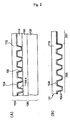
- the shape of the protrusion/depression pattern formed on each stamper was confirmed by inspection using an AFM (atomic force microscope).
- a silicon nitride (SiN) probe tip was used for the AFM probe. Measurement was conducted using a noncontact mode, and the variations in atomic force between the sample and the probe were converted to an image.
- Fig. 3(A) shows the AFM image of the stamper No. 1
- Fig. 3(B) is a line diagram showing the cross-sectional shape of the same image
- Fig. 4(A) shows the AFM image of the stamper No. 2
- Fig. 4(B) is a line diagram showing the cross-sectional shape of the same image.
- the dark areas of high dot density represent the concave sections within the protrusion/depression patterns
- the areas of low dot density or the white areas represent the convex sections
- these concave and convex sections correspond with the convex and concave sections respectively of the protrusion/depression pattern on the photoresist master.
- the protrusion/depression patterns are formed with a pitch of 0.32 ⁇ m.
- the light absorption layer contacting the photoresist layer enables the formation of a sharp protrusion/depression pattern on the photoresist master, and the Pd provided on the surface of this protrusion/depression pattern enables the production of a stamper that is faithful to this protrusion/depression pattern.
Landscapes
- Engineering & Computer Science (AREA)
- Manufacturing & Machinery (AREA)
- Physics & Mathematics (AREA)
- General Physics & Mathematics (AREA)
- Manufacturing Optical Record Carriers (AREA)
- Length Measuring Devices By Optical Means (AREA)
- Moulds For Moulding Plastics Or The Like (AREA)
Applications Claiming Priority (3)
| Application Number | Priority Date | Filing Date | Title |
|---|---|---|---|
| JP2001398994 | 2001-12-28 | ||
| JP2001398994 | 2001-12-28 | ||
| PCT/JP2002/013876 WO2003058613A1 (fr) | 2001-12-28 | 2002-12-27 | Procede de fabrication d'une matrice de pressage pour support d'informations, matrice de pressage et disque original photosensible |
Publications (1)
| Publication Number | Publication Date |
|---|---|
| EP1460626A1 true EP1460626A1 (fr) | 2004-09-22 |
Family
ID=19189414
Family Applications (1)
| Application Number | Title | Priority Date | Filing Date |
|---|---|---|---|
| EP02790950A Withdrawn EP1460626A1 (fr) | 2001-12-28 | 2002-12-27 | Procede de fabrication d'une matrice de pressage pour support d'informations, matrice de pressage et disque original photosensible |
Country Status (5)
| Country | Link |
|---|---|
| US (1) | US20050066825A1 (fr) |
| EP (1) | EP1460626A1 (fr) |
| AU (1) | AU2002367345A1 (fr) |
| TW (1) | TW200301478A (fr) |
| WO (1) | WO2003058613A1 (fr) |
Families Citing this family (6)
| Publication number | Priority date | Publication date | Assignee | Title |
|---|---|---|---|---|
| KR20030078085A (ko) * | 2001-02-27 | 2003-10-04 | 티디케이가부시기가이샤 | 광정보매체용 포토레지스트원반의 제조방법 및광정보매체용 스탬퍼의 제조방법 |
| JP2003085829A (ja) * | 2001-09-06 | 2003-03-20 | Tdk Corp | 光情報媒体用スタンパの製造方法およびこれに用いるフォトレジスト原盤、ならびに、光情報媒体用スタンパおよび光情報媒体 |
| TWI228718B (en) * | 2001-11-05 | 2005-03-01 | Tdk Corp | Manufacturing method and device of mold plate for information medium |
| WO2003046904A1 (fr) * | 2001-11-30 | 2003-06-05 | Tdk Corporation | Procede et dispositif de matriçage et de pressage de supports d'information |
| TWI258142B (en) * | 2002-01-08 | 2006-07-11 | Tdk Corp | Manufacturing method of stamper for manufacturing data medium, the stamper, and the stamper spacer with template |
| JPWO2003077239A1 (ja) * | 2002-03-11 | 2005-07-07 | Tdk株式会社 | フォトレジスト原盤の加工方法、記録媒体用原盤の製造方法、記録媒体の製造方法、フォトレジスト原盤、記録媒体用原盤及び記録媒体 |
Family Cites Families (16)
| Publication number | Priority date | Publication date | Assignee | Title |
|---|---|---|---|---|
| JP2881871B2 (ja) * | 1989-12-08 | 1999-04-12 | ソニー株式会社 | 光ディスクの原盤作成方法 |
| JPH04263140A (ja) * | 1991-02-07 | 1992-09-18 | Ricoh Co Ltd | 無反射コート付きガラス原盤 |
| JPH05214547A (ja) * | 1992-01-31 | 1993-08-24 | Sony Corp | 無電解めっき方法 |
| JPH06215422A (ja) * | 1993-01-14 | 1994-08-05 | Sony Corp | スタンパーの製造方法及びスタンパー |
| JPH08185643A (ja) * | 1994-12-30 | 1996-07-16 | Sony Corp | デイスク原盤作成装置 |
| JPH08273219A (ja) * | 1995-03-30 | 1996-10-18 | Sony Corp | 光ディスクの製造装置 |
| WO1996032521A1 (fr) * | 1995-04-10 | 1996-10-17 | Kao Corporation | Procede de metallisation au bain chaud, et procede et equipement de production de matrices |
| JPH08283950A (ja) * | 1995-04-10 | 1996-10-29 | Kao Corp | 無電解めっき方法及びスタンパーの製造方法 |
| JPH09109276A (ja) * | 1995-10-17 | 1997-04-28 | Kao Corp | 光ディスク用のスタンパーの製造方法 |
| JP3436843B2 (ja) * | 1996-04-25 | 2003-08-18 | 東京応化工業株式会社 | リソグラフィー用下地材及びそれを用いたリソグラフィー用レジスト材料 |
| JP2000280255A (ja) * | 1999-03-31 | 2000-10-10 | Seiko Epson Corp | 原盤の製造方法 |
| JP2001184734A (ja) * | 1999-12-24 | 2001-07-06 | Hitachi Maxell Ltd | 情報記録媒体用基板を製造するための原盤及びその製造方法 |
| JP2001357567A (ja) * | 2000-04-14 | 2001-12-26 | Tdk Corp | 光ディスク原盤の製造方法 |
| TWI254306B (en) * | 2002-01-08 | 2006-05-01 | Tdk Corp | Manufacturing method of stamper for manufacturing data medium, the stamper, and the photoresist template |
| TWI264717B (en) * | 2002-01-08 | 2006-10-21 | Tdk Corp | Manufacturing method of stamper for manufacturing data medium, the stamper, and the photoresist template |
| US7074341B1 (en) * | 2002-07-01 | 2006-07-11 | Seagate Technology Llc | Method for protecting surface of stamper/imprinter during manufacture thereof |
-
2002
- 2002-12-27 US US10/500,008 patent/US20050066825A1/en not_active Abandoned
- 2002-12-27 AU AU2002367345A patent/AU2002367345A1/en not_active Abandoned
- 2002-12-27 WO PCT/JP2002/013876 patent/WO2003058613A1/fr not_active Ceased
- 2002-12-27 TW TW091137734A patent/TW200301478A/zh unknown
- 2002-12-27 EP EP02790950A patent/EP1460626A1/fr not_active Withdrawn
Non-Patent Citations (1)
| Title |
|---|
| See references of WO03058613A1 * |
Also Published As
| Publication number | Publication date |
|---|---|
| WO2003058613A1 (fr) | 2003-07-17 |
| TW200301478A (en) | 2003-07-01 |
| AU2002367345A1 (en) | 2003-07-24 |
| US20050066825A1 (en) | 2005-03-31 |
Similar Documents
| Publication | Publication Date | Title |
|---|---|---|
| US20050042427A1 (en) | Method for manufacturing stamper for information medium manufacture, stamper, and stamper intermediate with master disk | |
| EP1460625A1 (fr) | Procede et dispositif de matricage et de pressage de supports d'information | |
| US7204188B2 (en) | Method of manufacturing stamper for manufacturing information medium, stamper, and photoresist master | |
| EP1460626A1 (fr) | Procede de fabrication d'une matrice de pressage pour support d'informations, matrice de pressage et disque original photosensible | |
| US6127100A (en) | Method of manufacturing a stamper for use in optical information recording medium | |
| EP1465174A1 (fr) | Procede de fabrication de matrice pour faconnage de support d'information, matrice et disque maitre de photoresine | |
| JPH0453015B2 (fr) | ||
| EP1450361A1 (fr) | Procede et dispositif de fabrication d'une matrice de pressage pour support d'information | |
| JP2000280255A (ja) | 原盤の製造方法 | |
| JPH11259910A (ja) | 光ディスクおよびその原盤製造方法 | |
| US20080241525A1 (en) | Stamper for optical information recording medium, master for magnetic transfer, and manufacturing methods thereof | |
| JP3749520B2 (ja) | 情報媒体製造用スタンパの製造方法、スタンパ、及び原盤付スタンパ中間体 | |
| US6071586A (en) | Manufacturing method of a master disk for forming an optical disk, and the master disk | |
| CN101714370B (zh) | 生产光盘的方法和生产压模的方法 | |
| JP2003085829A (ja) | 光情報媒体用スタンパの製造方法およびこれに用いるフォトレジスト原盤、ならびに、光情報媒体用スタンパおよび光情報媒体 | |
| JP2003272249A (ja) | 情報媒体製造用スタンパの製造方法、スタンパ及びフォトレジスト原盤 | |
| JPH11350181A (ja) | スタンパの製造方法 | |
| JP3186078B2 (ja) | マスタリング方法、スタンパおよび光記録媒体 | |
| JP2003257090A (ja) | 情報媒体製造用スタンパの製造方法、スタンパ及びフォトレジスト原盤 | |
| US20080241308A1 (en) | Stamper for optical information recording medium, master for magnetic transfer, and manufacturing methods thereof | |
| JP3186079B2 (ja) | マスタリング方法、スタンパおよび光記録媒体 | |
| JP2003272255A (ja) | 情報媒体製造用スタンパの製造方法、スタンパ及びフォトレジスト原盤 | |
| US20040166446A1 (en) | Method for manufacturing metal master of information recording disc and metal master | |
| JP2001243662A (ja) | 記録媒体の製造方法、および記録媒体製造用原盤の製造方法 | |
| JP2800447B2 (ja) | スタンパの製造方法及び光ディスクの製造方法 |
Legal Events
| Date | Code | Title | Description |
|---|---|---|---|
| PUAI | Public reference made under article 153(3) epc to a published international application that has entered the european phase |
Free format text: ORIGINAL CODE: 0009012 |
|
| 17P | Request for examination filed |
Effective date: 20040628 |
|
| AK | Designated contracting states |
Kind code of ref document: A1 Designated state(s): AT BE BG CH CY CZ DE DK EE ES FI FR GB GR IE IT LI LU MC NL PT SE SI SK TR |
|
| AX | Request for extension of the european patent |
Extension state: AL LT LV MK RO |
|
| STAA | Information on the status of an ep patent application or granted ep patent |
Free format text: STATUS: THE APPLICATION HAS BEEN WITHDRAWN |
|
| 18W | Application withdrawn |
Effective date: 20051216 |