EP1469523A1 - Elektronisches Bauteil mit Übergang und mit dem Bauteil integriertes Leistungs-Bauelement - Google Patents
Elektronisches Bauteil mit Übergang und mit dem Bauteil integriertes Leistungs-Bauelement Download PDFInfo
- Publication number
- EP1469523A1 EP1469523A1 EP03425242A EP03425242A EP1469523A1 EP 1469523 A1 EP1469523 A1 EP 1469523A1 EP 03425242 A EP03425242 A EP 03425242A EP 03425242 A EP03425242 A EP 03425242A EP 1469523 A1 EP1469523 A1 EP 1469523A1
- Authority
- EP
- European Patent Office
- Prior art keywords
- region
- regions
- type semiconductor
- junction
- resistive
- Prior art date
- Legal status (The legal status is an assumption and is not a legal conclusion. Google has not performed a legal analysis and makes no representation as to the accuracy of the status listed.)
- Granted
Links
- 239000004065 semiconductor Substances 0.000 claims abstract description 22
- 239000003989 dielectric material Substances 0.000 claims 1
- 210000000746 body region Anatomy 0.000 description 7
- 229910021420 polycrystalline silicon Inorganic materials 0.000 description 7
- 230000015556 catabolic process Effects 0.000 description 6
- 230000000875 corresponding effect Effects 0.000 description 6
- 229920005591 polysilicon Polymers 0.000 description 5
- 238000010586 diagram Methods 0.000 description 4
- 238000004804 winding Methods 0.000 description 4
- 230000008901 benefit Effects 0.000 description 3
- 239000002184 metal Substances 0.000 description 3
- WYTGDNHDOZPMIW-RCBQFDQVSA-N alstonine Natural products C1=CC2=C3C=CC=CC3=NC2=C2N1C[C@H]1[C@H](C)OC=C(C(=O)OC)[C@H]1C2 WYTGDNHDOZPMIW-RCBQFDQVSA-N 0.000 description 2
- 238000002485 combustion reaction Methods 0.000 description 2
- 230000002596 correlated effect Effects 0.000 description 2
- 230000010355 oscillation Effects 0.000 description 2
- 230000003071 parasitic effect Effects 0.000 description 2
- 230000004913 activation Effects 0.000 description 1
- 238000001994 activation Methods 0.000 description 1
- 230000007423 decrease Effects 0.000 description 1
- 238000001514 detection method Methods 0.000 description 1
- 230000000694 effects Effects 0.000 description 1
- 230000005669 field effect Effects 0.000 description 1
- 238000002513 implantation Methods 0.000 description 1
- 230000010354 integration Effects 0.000 description 1
- 238000004519 manufacturing process Methods 0.000 description 1
- 230000000873 masking effect Effects 0.000 description 1
- 238000000034 method Methods 0.000 description 1
- 238000012986 modification Methods 0.000 description 1
- 230000004048 modification Effects 0.000 description 1
- 229910052710 silicon Inorganic materials 0.000 description 1
- 239000010703 silicon Substances 0.000 description 1
- 239000000758 substrate Substances 0.000 description 1
- 230000009466 transformation Effects 0.000 description 1
Images


Classifications
-
- H—ELECTRICITY
- H10—SEMICONDUCTOR DEVICES; ELECTRIC SOLID-STATE DEVICES NOT OTHERWISE PROVIDED FOR
- H10D—INORGANIC ELECTRIC SEMICONDUCTOR DEVICES
- H10D8/00—Diodes
- H10D8/20—Breakdown diodes, e.g. avalanche diodes
- H10D8/25—Zener diodes
-
- H—ELECTRICITY
- H10—SEMICONDUCTOR DEVICES; ELECTRIC SOLID-STATE DEVICES NOT OTHERWISE PROVIDED FOR
- H10D—INORGANIC ELECTRIC SEMICONDUCTOR DEVICES
- H10D12/00—Bipolar devices controlled by the field effect, e.g. insulated-gate bipolar transistors [IGBT]
- H10D12/411—Insulated-gate bipolar transistors [IGBT]
- H10D12/441—Vertical IGBTs
-
- H—ELECTRICITY
- H10—SEMICONDUCTOR DEVICES; ELECTRIC SOLID-STATE DEVICES NOT OTHERWISE PROVIDED FOR
- H10D—INORGANIC ELECTRIC SEMICONDUCTOR DEVICES
- H10D62/00—Semiconductor bodies, or regions thereof, of devices having potential barriers
- H10D62/10—Shapes, relative sizes or dispositions of the regions of the semiconductor bodies; Shapes of the semiconductor bodies
- H10D62/124—Shapes, relative sizes or dispositions of the regions of semiconductor bodies or of junctions between the regions
- H10D62/126—Top-view geometrical layouts of the regions or the junctions
- H10D62/127—Top-view geometrical layouts of the regions or the junctions of cellular field-effect devices, e.g. multicellular DMOS transistors or IGBTs
-
- H—ELECTRICITY
- H10—SEMICONDUCTOR DEVICES; ELECTRIC SOLID-STATE DEVICES NOT OTHERWISE PROVIDED FOR
- H10D—INORGANIC ELECTRIC SEMICONDUCTOR DEVICES
- H10D84/00—Integrated devices formed in or on semiconductor substrates that comprise only semiconducting layers, e.g. on Si wafers or on GaAs-on-Si wafers
- H10D84/201—Integrated devices formed in or on semiconductor substrates that comprise only semiconducting layers, e.g. on Si wafers or on GaAs-on-Si wafers characterised by the integration of only components covered by H10D1/00 or H10D8/00, e.g. RLC circuits
- H10D84/204—Integrated devices formed in or on semiconductor substrates that comprise only semiconducting layers, e.g. on Si wafers or on GaAs-on-Si wafers characterised by the integration of only components covered by H10D1/00 or H10D8/00, e.g. RLC circuits of combinations of diodes or capacitors or resistors
-
- H—ELECTRICITY
- H10—SEMICONDUCTOR DEVICES; ELECTRIC SOLID-STATE DEVICES NOT OTHERWISE PROVIDED FOR
- H10D—INORGANIC ELECTRIC SEMICONDUCTOR DEVICES
- H10D89/00—Aspects of integrated devices not covered by groups H10D84/00 - H10D88/00
- H10D89/60—Integrated devices comprising arrangements for electrical or thermal protection, e.g. protection circuits against electrostatic discharge [ESD]
- H10D89/601—Integrated devices comprising arrangements for electrical or thermal protection, e.g. protection circuits against electrostatic discharge [ESD] for devices having insulated gate electrodes, e.g. for IGFETs or IGBTs
- H10D89/611—Integrated devices comprising arrangements for electrical or thermal protection, e.g. protection circuits against electrostatic discharge [ESD] for devices having insulated gate electrodes, e.g. for IGFETs or IGBTs using diodes as protective elements
-
- H—ELECTRICITY
- H10—SEMICONDUCTOR DEVICES; ELECTRIC SOLID-STATE DEVICES NOT OTHERWISE PROVIDED FOR
- H10D—INORGANIC ELECTRIC SEMICONDUCTOR DEVICES
- H10D62/00—Semiconductor bodies, or regions thereof, of devices having potential barriers
- H10D62/10—Shapes, relative sizes or dispositions of the regions of the semiconductor bodies; Shapes of the semiconductor bodies
- H10D62/124—Shapes, relative sizes or dispositions of the regions of semiconductor bodies or of junctions between the regions
- H10D62/126—Top-view geometrical layouts of the regions or the junctions
Definitions
- the present invention relates to a junction electronic component and to an integrated power device incorporating said component.
- IGBTs insulated-gate bipolar transistors
- driver devices which, among other things, operate to prevent overvoltages or undesirable oscillations on the high-voltage terminals, which may cause serious problems.
- IGBTs are normally used as power switches for supplying the primary windings of the high-voltage transformers.
- the primary winding of one of the high-voltage transformers is supplied with a constant battery voltage and hence is traversed by a current which increases in time.
- a clamp circuit intervenes to limit said current when the energy stored in the primary winding is sufficient to cause a spark between the electrodes of a spark-plug connected to the secondary winding of the same transformer.
- the opening of the circuit by the power switch causes a voltage peak (normally comprised between 400 V and 600 V), which, amplified by the transformation ratio of the transformer, causes the spark.
- a voltage peak normally comprised between 400 V and 600 V
- the voltage on the collector of the IGBT must be controlled both upon switching-off of the IGBT itself, to prevent any possible breakdown, and when the limiting circuit intervenes; in the absence of control, in fact, so large oscillations may occur as to cause undesirable sparks.
- the driver device associated to the power device with a signal representing the voltage present on the high-voltage terminal (the collector terminal, in the case of IGBTs); on the basis of this signal, the driving device acts on a control terminal of the power device.
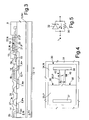
- FIG. 1 shows an IGBT 1 made in a semiconductor body and comprising a collector region 3, a conduction region 5, body regions 6, emitter regions 7, a gate region 8, an equipotential region 9, and a protection circuit 10.
- the collector region 3 is formed in a substrate of the body 2, here of P+ type, and has a face coated with a metal layer forming a collector contact 11.
- the conduction region 5, which is of N- type, extends above the collector region 3 and is separated therefrom by a junction layer 13, of N+ type. Furthermore, the collector region 3 and the conduction region 5 are high-voltage regions.
- the body regions 6, of P+ type are housed in the conduction region 5 and emerge on a surface 5a of the conduction region itself.
- the body regions 6 house the emitter regions 7, which are of an N+ type and which are also substantially flush with the surface 5a.
- all of the emitter regions 7 are connected to a single emitter contact 14.
- the gate region 8 which is made of polysilicon, is insulated from the conduction region 5 by means of a thin layer of gate oxide 15, and from the emitter contact 14 by means of an insulating layer 16. Furthermore, the gate region 8 comprises a first portion 8a, provided with a gate contact 19, and second biasing portions 8b (the first and the second portions 8a, 8b are connected together; however, the connection is not visible in the cross-sectional view of Figure 1). The second portions 8b of the gate region 8 extend between adjacent body regions 6 and partially overlap the emitter regions 7.
- the equipotential region 9, which is normally metallic, is in direct electrical connection with the conduction region 5 and extends on its surface 5a around the IGBT 1.
- the voltage of the conduction region 5 and of the equipotential region 9 differ from the voltage of the collector region 3 only by the forward voltage present on the PN junction formed by the collector region 3 and by the junction region 13. For this reason, the equipotential region 9 is used as a sensor for detection of the collector voltage.
- the protection device 10 is connected to the gate contact 19 and to the equipotential region 9 and comprises a cascade of Zener diodes 20 connected in pairs in back-to-back configuration, i.e., having cathode terminals in common.
- the Zener diodes are formed by means of first and second strips 21, 22 of polysilicon, which are contiguous and have alternated P type and N type conductivity (see Figure 2). More precisely, each first strip 21, having for example P type conductivity, is contiguous to two second strips 22 having N type conductivity; instead, each second strip 22 is contiguous to two first strips 21.
- the Zener diodes 20 are formed by the junctions 23 between adjacent strips 21, 22.
- each first strip 21, having P type conductivity constitutes a common anode terminal of two adjacent Zener diodes 20; likewise, each second strip 22, having N type conductivity, constitutes a common cathode terminal of two adjacent Zener diodes 20.
- the protection device 10 is moreover made on a thick field-oxide region 25 and hence is electrically connected to the conduction region 5 only through the equipotential region 9. In practice, the protection device 10 limits the voltage between the gate region 8 and the equipotential region 9 to a maximum value equal to the sum of the reverse breakdown voltages of the equi-oriented Zener diodes 20 (i.e., half of the total number of the Zener diodes 20).
- the terminal used as high-voltage sensor i.e., the equipotential region 9
- the terminal used as high-voltage sensor i.e., the equipotential region 9
- the terminal used as high-voltage sensor is in turn a high-voltage terminal and hence can be connected only to control devices capable of withstanding and processing voltages of several hundreds of volts.
- JFET junction field-effect transistor
- the JFET 27 has an emitter contact 28, formed on a portion 5a of the conduction region 5, which is delimited laterally by two body regions 6.
- the body regions 6 and the conduction region 5 are used as gate regions and, respectively, as drain region of the JFET 27, while the emitter contact 14 functions also as gate contact.
- the current flowing through the JFET 27 is modulated by the voltage present between the conduction region 5 and the emitter contact 14.
- the output of the voltage sensor is advantageously a current, which can be easily converted into a low-voltage signal.
- the presence of a transistor within the conduction region 5 introduces active parasitic components, with consequent problems as regards possible undesired activations (latch-up) and tends to modify the behaviour of the power device.
- the overall dimensions increase.
- the aim of the present invention is to provide a junction electronic component which can be used as a high-voltage sensor, and an integrated power device incorporating said junction electronic component, which are free from the drawbacks described.
- junction electronic component and a high-power integrated device incorporating said junction electronic component as claimed in according to any one of Claim 1 and Claim 10, respectively.
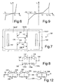
- a junction electronic component is designated by the number 30, which is integrated in a semiconductor body 31, for example made of silicon, and comprises a Zener diode 32 and an integrated resistive region 35.
- the Zener diode 32 comprises an anode region 33, having conductivity of P type, and a cathode region 34, contiguous to the anode region 33 and having conductivity of N type.
- the anode and cathode regions 33, 34 have respective pre-determined doping levels and form a PN junction 36, which has a forward conduction voltage V F of approximately 0.7 V and a reverse breakdown voltage V B correlated to the doping levels.
- the reverse breakdown voltage V B is approximately 7.5 V.
- the anode and cathode regions 33, 34 are provided with respective metal anode and cathode contacts 37, 38, opposite to the PN junction 36, for electrical connection of the junction component 30 to circuit components (here not illustrated).
- the integrated resistive region 35 which is also made of polysilicon, has the same type of conductivity (P) and, preferably, the same level of doping as the anode region 33. Furthermore, the integrated resistive region 35 is shaped like a strip of pre-determined width L, which projects from the anode region 33 in a direction substantially perpendicular to the PN junction 36 and extends through the cathode region 34, as far as underneath the cathode contact 38. In other words, the integrated resistive region 35 and the cathode contact 38 are in direct electrical connection with one another. In this way, in practice, a resistive path connects together the anode and cathode contacts 37. 38, in parallel to the PN junction 36 ( Figure 5).
- the junction component 30 has the characteristic illustrated in Figure 6.
- the work current I D flowing through the junction component 30 depends substantially in a linear way on the work voltage V D applied between the anode and cathode terminals 37, 38 when said work voltage V D is comprised between -
- the relation between work voltage V D and work current I D is not exactly linear even for weak reverse voltages.
- the integrated resistive region 35 and the cathode region 34 are contiguous to one another, and hence PN junctions are formed along the edges 40 of the integrated resistive region 35 itself.
- a reverse voltage is set up which causes partial emptying of the integrated resistive region 35. Consequently, the pre-determined effective width L E of the integrated resistive region 35 decreases, and its resistivity increases.
- the integrated resistive region 35 tends to present the so-called "pinch-off" typical of JFETs.
- junction electronic component according to the invention may advantageously be used in all the cases in which it is necessary to provide a controlled passage of current through the anode and cathode terminals of a polysilicon diode. Owing to the integration of the resistive region directly within the diode, the junction component is extremely compact and enables a considerable saving of area. A further advantage is provided in that the resistivity value of the integrated resistive regions is practically independent of the temperature, with the normal doping levels.
- junction component described is particularly suited for modular usein making pairs of diodes in back-to-back configuration and high-voltage sensors, as illustrated hereinafter.
- a junction component 130 comprises: a first anode region 132 and a second anode region 133, both having conductivity of P type; a cathode region 134, contiguous to both of the anode regions 133 and having conductivity of N type; and an integrated resistive region 135, having the same conductivity as the anode regions 133.
- the first and the second anode regions 132, 133 form, with the cathode region 134, a first Zener diode 137 and a second Zener diode 138 identical to one another and facing in opposite directions (in back-to-back configuration, see Figure 8).
- the first Zener diode 137 comprises a first PN junction 140, defined between the first anode region 132 and the cathode region 134
- the second Zener diode 138 comprises a second PN junction 141, defined between the second anode region 133 and the cathode region 134; the cathode region 134 is thus common to the Zener diodes 137, 138.
- Metal contacts 142 are made at opposite ends of the first and of the second anode regions 132, 133 and hence are opposite to the PN junctions 140, 141.
- the integrated resistive region 135 extends between the first and the second anode regions 132, 133 across the cathode region 134 ( Figure 7).
- the integrated resistive region 135 is substantially perpendicular to the PN junctions 140, 141, has a pre-determined width L', and is contiguous to the cathode region 134 along its edges 143.
- the integrated resistive region 135 defines a resistive path parallel to the first Zener diode 137 and to the second Zener diode 138 and connecting the contacts 142 ( Figure 8).
- an intermediate point 135a of the resistive region 135 itself is at the potential of the cathode region 134.
- the characteristic of the junction component 130 is substantially symmetrical.
- the absolute value of the work voltage V D ' is lower than the forward conduction voltage V F ' (approximately 0.7 V) of the Zener diodes 137, 138
- the work current I D ' flows between the contacts 142 only through the integrated resistive region 135. Consequently, the work voltage V D ' and the work current I D ' are linked by a substantially linear relation.
- the Zener diodes 137, 138 are on.
- V B ' the reverse breakdown voltage (approximately 7.5 V) of the PN junctions 140, 141, when we have:
- the slope of the characteristic of the junction component 130 is determined substantially by the portion 135b, 135c of the integrated resistive region parallel to the inhibited Zener diode 137, 138.
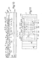
- the IGBT 200 comprises the collector region 3, the conduction region 5, the body regions 6, the emitter regions 7, the gate region 8 with the gate contact 19, the equipotential region 9, and a junction component 230, which is used as high-voltage sensor.
- the junction component 230 is separated from the conduction region 5 by means of the field-oxide layer 25 and is connected between the equipotential region 9 and the gate contact 19.
- the junction component 230 made of polycrystalline silicon, comprises: a plurality of anode regions 233 having conductivity of a P type; a plurality of cathode regions 234 having conductivity of an N type; and a plurality of integrated resistive regions 235, here of a P type.
- the gate contact 19 and the portion of the equipotential region 9 that contacts the junction component 230 are illustrated with a dashed line.
- the anode regions 233 and the cathode regions 234 are alternate and in contiguous pairs so as to form a plurality of first and second Zener diodes 237, 238, which are identical to one another and comprise respective PN junctions 236.
- the first Zener diodes 237 are alternated with the second Zener diodes 238 so that a first Zener diode 237 and a second Zener diode 238 adjacent to one another are connected together in back-to-back configuration.
- each of the anode regions 233 and of the cathode regions 234 is common to a respective first Zener diode 237 and to a respective second Zener diode 238.
- each PN junction 236 functions as a biasing region for the adjacent PN junctions 236.
- the integrated resistive regions 235 extend between two successive anode regions 233 perpendicular to the PN junctions 236 and traverse the corresponding cathode region 234. Each integrated resistive region 235 thus forms a resistive path parallel to corresponding first and second Zener diodes 237, 238. Furthermore, the integrated resistive regions 235, which in the embodiment described are aligned, define a resistive path connecting the gate contact 19 and the equipotential region 9; in particular, each integrated resistive region 236 is in parallel to a corresponding PN junction 236 (see also Figure 12).
- a sensing current I S flows through the junction component 230 ( Figure 13), and is correlated to the voltage of the conduction region 5 and hence to the collector voltage V C present on the collector contact 11 (as mentioned previously, in fact, these voltages differ by an amount equal to the forward biasing voltage of a PN junction, i.e., approximately 0.7 V).
- the sensing current I S depends in a substantially piecewise-linear way upon the collector voltage V C (high voltage) when the collector voltage V C is lower, in absolute value, than a clamp voltage V LIM equal to N*(
- the junction component 230 moreover limits the collector voltage V C to the clamp voltage V LIM ; once said voltage has been reached, the sensing current I S is substantially independent of the collector voltage V C (the contribution due to the current flowing through the integrated resistive regions 235 is substantially negligible).
- the value of the clamp voltage V LIM depends upon the number N of first Zener diodes 237 or of second Zener diodes 238 present and is normally comprised between 400 V and 600 V.
- the sensing current I S is supplied to the gate contact and can be conveniently taken and converted into a low-voltage signal indicative of the collector voltage V C (high voltage). Consequently, it is advantageously possible to associate to the IGBT 200 standard control circuits, and it is not necessary to provide devices capable of processing high voltages.
- the junction component 230 does not introduce parasitic structures into the IGBT 200, as it is made of polysilicon above a thick oxide layer (field oxide) outside of the active area. Furthermore, the clamp voltage V LIM of the junction component 230 may be conveniently controlled by selecting an appropriate number of Zener diodes. Another advantage is that the integrated resistive regions 235 may be used as intermediate sensing points since the voltage varies gradually along the resistive path between the equipotential region 9 and the gate contact 19.
- a junction component 330 made of polycrystalline silicon, comprises anode regions 333, having conductivity of a P type, cathode regions 334, having conductivity of a N type, and integrated resistive regions 335.
- the junction component 330 is connected between the equipotential region 9 and the gate contact 19 of an IGBT (here not illustrated).
- the anode region 333 and cathode region 334 are alternated and contiguous in pairs so as to form first and second Zener diodes 337, 338 comprising respective PN junctions 336.
- Each of the anode and cathode regions 333, 334 is common to a pair of adjacent first and second Zener diodes 337, 338, which are connected in back-to-back configuration ( Figure 15).
- the integrated resistive regions 335 which are of a P type, extend between consecutive anode regions 333 in a direction substantially perpendicular to the PN junctions 336.
- the integrated resistive regions 336 are staggered with respect to one another and, preferably, are arranged alongside the corresponding cathode regions 334 alternately along first and second opposite edges 340, 341 of the cathode regions 334 themselves. Consequently, the integrated resistive regions 335 are contiguous to the corresponding cathode regions 334 on just one side, and a serpentine resistive path is formed, which connects the equipotential region 9 and the gate contact 19 and also includes the anode regions 333. Furthermore, each integrated resistive region 336 is in parallel with the corresponding PN junction 336.
- the greater length of the serpentine resistive path represents a further advantage of the junction component 330: in fact, the overall resistance in parallel to the Zener diodes 337, 338 is increased, given the same area occupied.
- the integrated resistive regions could have a different conformation with respect to what has been described above (for example, the ratio between the width and the length could be different).
- the integrated resistive regions could have the same type of conductivity as the cathode regions and extend from the cathode regions through the anode regions.
- the doping level of the integrated resistive regions could be different from the doping levels both of the anode regions and of the cathode regions (for this purpose, the fabrication of the junction component could envisage implantation and possibly masking steps specifically for doping the integrated resistive regions).
Landscapes
- Metal-Oxide And Bipolar Metal-Oxide Semiconductor Integrated Circuits (AREA)
- Semiconductor Integrated Circuits (AREA)
Priority Applications (4)
| Application Number | Priority Date | Filing Date | Title |
|---|---|---|---|
| EP03425242A EP1469523B1 (de) | 2003-04-18 | 2003-04-18 | Elektronisches Bauteil mit Übergang und mit dem Bauteil integriertes Leistungs-Bauelement |
| DE60325458T DE60325458D1 (de) | 2003-04-18 | 2003-04-18 | Elektronisches Bauteil mit Übergang und mit dem Bauteil integriertes Leistungs-Bauelement |
| JP2004106240A JP2004356622A (ja) | 2003-04-18 | 2004-03-31 | 接合型電子部品および前記電子部品を含む集積された電力装置 |
| US10/817,742 US7091559B2 (en) | 2003-04-18 | 2004-04-01 | Junction electronic component and an integrated power device incorporating said component |
Applications Claiming Priority (1)
| Application Number | Priority Date | Filing Date | Title |
|---|---|---|---|
| EP03425242A EP1469523B1 (de) | 2003-04-18 | 2003-04-18 | Elektronisches Bauteil mit Übergang und mit dem Bauteil integriertes Leistungs-Bauelement |
Publications (2)
| Publication Number | Publication Date |
|---|---|
| EP1469523A1 true EP1469523A1 (de) | 2004-10-20 |
| EP1469523B1 EP1469523B1 (de) | 2008-12-24 |
Family
ID=32893035
Family Applications (1)
| Application Number | Title | Priority Date | Filing Date |
|---|---|---|---|
| EP03425242A Expired - Lifetime EP1469523B1 (de) | 2003-04-18 | 2003-04-18 | Elektronisches Bauteil mit Übergang und mit dem Bauteil integriertes Leistungs-Bauelement |
Country Status (4)
| Country | Link |
|---|---|
| US (1) | US7091559B2 (de) |
| EP (1) | EP1469523B1 (de) |
| JP (1) | JP2004356622A (de) |
| DE (1) | DE60325458D1 (de) |
Families Citing this family (15)
| Publication number | Priority date | Publication date | Assignee | Title |
|---|---|---|---|---|
| JP3679097B2 (ja) | 2002-05-31 | 2005-08-03 | 株式会社光波 | 発光素子 |
| US7511357B2 (en) * | 2007-04-20 | 2009-03-31 | Force-Mos Technology Corporation | Trenched MOSFETs with improved gate-drain (GD) clamp diodes |
| US8085009B2 (en) | 2007-08-13 | 2011-12-27 | The Powerwise Group, Inc. | IGBT/FET-based energy savings device for reducing a predetermined amount of voltage using pulse width modulation |
| US8619443B2 (en) | 2010-09-29 | 2013-12-31 | The Powerwise Group, Inc. | System and method to boost voltage |
| US8120307B2 (en) | 2007-08-24 | 2012-02-21 | The Powerwise Group, Inc. | System and method for providing constant loading in AC power applications |
| US8810190B2 (en) | 2007-09-14 | 2014-08-19 | The Powerwise Group, Inc. | Motor controller system and method for maximizing energy savings |
| US8698447B2 (en) | 2007-09-14 | 2014-04-15 | The Powerwise Group, Inc. | Energy saving system and method for devices with rotating or reciprocating masses |
| US8004255B2 (en) | 2008-08-07 | 2011-08-23 | The Powerwise Group, Inc. | Power supply for IGBT/FET drivers |
| US8164162B2 (en) * | 2009-06-11 | 2012-04-24 | Force Mos Technology Co., Ltd. | Power semiconductor devices integrated with clamp diodes sharing same gate metal pad |
| CN102498294B (zh) | 2009-09-08 | 2015-08-12 | 智能动力股份有限公司 | 用于带有旋转或往复运动块的装置的节能系统和方法 |
| US8698446B2 (en) | 2009-09-08 | 2014-04-15 | The Powerwise Group, Inc. | Method to save energy for devices with rotating or reciprocating masses |
| WO2013015014A1 (ja) * | 2011-07-22 | 2013-01-31 | 富士電機株式会社 | 超接合半導体装置 |
| JP6512025B2 (ja) | 2015-08-11 | 2019-05-15 | 富士電機株式会社 | 半導体素子及び半導体素子の製造方法 |
| CN106558580B (zh) * | 2015-09-30 | 2019-12-10 | 无锡华润上华科技有限公司 | 具有静电释放保护结构的半导体器件 |
| JP2018067570A (ja) * | 2016-10-17 | 2018-04-26 | 富士電機株式会社 | 半導体装置 |
Citations (7)
| Publication number | Priority date | Publication date | Assignee | Title |
|---|---|---|---|---|
| US3171042A (en) * | 1961-09-08 | 1965-02-23 | Bendix Corp | Device with combination of unipolar means and tunnel diode means |
| JPS62199051A (ja) * | 1986-02-27 | 1987-09-02 | Sumitomo Electric Ind Ltd | 半導体装置の入力保護回路 |
| JPS6350070A (ja) * | 1986-08-19 | 1988-03-02 | Matsushita Electronics Corp | 縦型mos電界効果トランジスタ |
| EP1028511A2 (de) * | 1999-02-14 | 2000-08-16 | Yazaki Corporation | Stromversorgungssystem mit aktiver Halbleitersicherung |
| US6268628B1 (en) * | 1998-04-03 | 2001-07-31 | Fuji Electric Co., Ltd. | Depletion type MOS semiconductor device and MOS power IC |
| EP1189286A1 (de) * | 2000-03-06 | 2002-03-20 | Rohm Co., Ltd. | Halbleiteranordnung |
| JP2002246598A (ja) * | 2001-02-15 | 2002-08-30 | Nec Yamagata Ltd | 半導体装置及びその製造方法 |
Family Cites Families (5)
| Publication number | Priority date | Publication date | Assignee | Title |
|---|---|---|---|---|
| JPS5621357A (en) * | 1979-07-27 | 1981-02-27 | Pioneer Electronic Corp | Integrated circuit device |
| JPH04369863A (ja) * | 1991-06-19 | 1992-12-22 | Matsushita Electric Ind Co Ltd | 半導体装置及びその製造方法 |
| JPH06252349A (ja) * | 1993-02-23 | 1994-09-09 | Seiko Epson Corp | 半導体装置及び半導体装置の製造方法 |
| JPH06342878A (ja) * | 1993-04-06 | 1994-12-13 | Fuji Electric Co Ltd | 半導体装置 |
| JP2001085682A (ja) * | 1999-09-10 | 2001-03-30 | Toyota Autom Loom Works Ltd | パワーmosトランジスタ |
-
2003
- 2003-04-18 EP EP03425242A patent/EP1469523B1/de not_active Expired - Lifetime
- 2003-04-18 DE DE60325458T patent/DE60325458D1/de not_active Expired - Lifetime
-
2004
- 2004-03-31 JP JP2004106240A patent/JP2004356622A/ja active Pending
- 2004-04-01 US US10/817,742 patent/US7091559B2/en not_active Expired - Lifetime
Patent Citations (7)
| Publication number | Priority date | Publication date | Assignee | Title |
|---|---|---|---|---|
| US3171042A (en) * | 1961-09-08 | 1965-02-23 | Bendix Corp | Device with combination of unipolar means and tunnel diode means |
| JPS62199051A (ja) * | 1986-02-27 | 1987-09-02 | Sumitomo Electric Ind Ltd | 半導体装置の入力保護回路 |
| JPS6350070A (ja) * | 1986-08-19 | 1988-03-02 | Matsushita Electronics Corp | 縦型mos電界効果トランジスタ |
| US6268628B1 (en) * | 1998-04-03 | 2001-07-31 | Fuji Electric Co., Ltd. | Depletion type MOS semiconductor device and MOS power IC |
| EP1028511A2 (de) * | 1999-02-14 | 2000-08-16 | Yazaki Corporation | Stromversorgungssystem mit aktiver Halbleitersicherung |
| EP1189286A1 (de) * | 2000-03-06 | 2002-03-20 | Rohm Co., Ltd. | Halbleiteranordnung |
| JP2002246598A (ja) * | 2001-02-15 | 2002-08-30 | Nec Yamagata Ltd | 半導体装置及びその製造方法 |
Non-Patent Citations (3)
| Title |
|---|
| PATENT ABSTRACTS OF JAPAN vol. 012, no. 054 (E - 583) 18 February 1988 (1988-02-18) * |
| PATENT ABSTRACTS OF JAPAN vol. 012, no. 268 (E - 638) 27 July 1988 (1988-07-27) * |
| PATENT ABSTRACTS OF JAPAN vol. 2002, no. 12 12 December 2002 (2002-12-12) * |
Also Published As
| Publication number | Publication date |
|---|---|
| EP1469523B1 (de) | 2008-12-24 |
| JP2004356622A (ja) | 2004-12-16 |
| DE60325458D1 (de) | 2009-02-05 |
| US20040262684A1 (en) | 2004-12-30 |
| US7091559B2 (en) | 2006-08-15 |
Similar Documents
| Publication | Publication Date | Title |
|---|---|---|
| US5079608A (en) | Power MOSFET transistor circuit with active clamp | |
| EP0505191B1 (de) | Halbleiterbauelement mit n-dotiertem Gebiet niedriger Konzentration zur Verbesserung der dV/dt Eigenschaften | |
| US5631187A (en) | Method for making semiconductor device having high energy sustaining capability and a temperature compensated sustaining voltage | |
| US6605844B2 (en) | Semiconductor device | |
| EP1469523B1 (de) | Elektronisches Bauteil mit Übergang und mit dem Bauteil integriertes Leistungs-Bauelement | |
| US5341003A (en) | MOS semiconductor device having a main unit element and a sense unit element for monitoring the current in the main unit element | |
| EP0110331B1 (de) | MOS-Transistor | |
| US4721986A (en) | Bidirectional output semiconductor field effect transistor and method for its maufacture | |
| US7916439B2 (en) | Semiconductor switch arrangement and an electronic device | |
| JP4971848B2 (ja) | 低スイッチング損失、低ノイズを両立するパワーmos回路 | |
| US11158627B2 (en) | Electronic circuit with a transistor device and a clamping circuit | |
| KR19990026902A (ko) | 정전기 보호회로 | |
| US7615812B1 (en) | Field effect semiconductor diodes and processing techniques | |
| US6914297B2 (en) | Configuration for generating a voltage sense signal in a power semiconductor component | |
| US5401996A (en) | Overvoltage protected semiconductor switch | |
| US20040046225A1 (en) | Semiconductor power component | |
| US5466952A (en) | Semiconductor device having an IGET and a control or protection component | |
| JP4858253B2 (ja) | トランジスタの駆動回路 | |
| US20070075367A1 (en) | SOI semiconductor component with increased dielectric strength | |
| JP4687385B2 (ja) | 電力変換装置 | |
| JP3146650B2 (ja) | パワー集積回路 | |
| JP2608975B2 (ja) | 半導体装置およびそれを用いたイグナイタ装置 | |
| KR100192956B1 (ko) | 전력 트랜지스터 |
Legal Events
| Date | Code | Title | Description |
|---|---|---|---|
| PUAI | Public reference made under article 153(3) epc to a published international application that has entered the european phase |
Free format text: ORIGINAL CODE: 0009012 |
|
| AK | Designated contracting states |
Kind code of ref document: A1 Designated state(s): AT BE BG CH CY CZ DE DK EE ES FI FR GB GR HU IE IT LI LU MC NL PT RO SE SI SK TR |
|
| AX | Request for extension of the european patent |
Extension state: AL LT LV MK |
|
| 17P | Request for examination filed |
Effective date: 20050418 |
|
| AKX | Designation fees paid |
Designated state(s): DE FR GB IT |
|
| GRAP | Despatch of communication of intention to grant a patent |
Free format text: ORIGINAL CODE: EPIDOSNIGR1 |
|
| GRAS | Grant fee paid |
Free format text: ORIGINAL CODE: EPIDOSNIGR3 |
|
| GRAA | (expected) grant |
Free format text: ORIGINAL CODE: 0009210 |
|
| AK | Designated contracting states |
Kind code of ref document: B1 Designated state(s): DE FR GB IT |
|
| REG | Reference to a national code |
Ref country code: GB Ref legal event code: FG4D |
|
| REF | Corresponds to: |
Ref document number: 60325458 Country of ref document: DE Date of ref document: 20090205 Kind code of ref document: P |
|
| PLBE | No opposition filed within time limit |
Free format text: ORIGINAL CODE: 0009261 |
|
| STAA | Information on the status of an ep patent application or granted ep patent |
Free format text: STATUS: NO OPPOSITION FILED WITHIN TIME LIMIT |
|
| 26N | No opposition filed |
Effective date: 20090925 |
|
| GBPC | Gb: european patent ceased through non-payment of renewal fee |
Effective date: 20090418 |
|
| PG25 | Lapsed in a contracting state [announced via postgrant information from national office to epo] |
Ref country code: GB Free format text: LAPSE BECAUSE OF NON-PAYMENT OF DUE FEES Effective date: 20090418 |
|
| PG25 | Lapsed in a contracting state [announced via postgrant information from national office to epo] |
Ref country code: IT Free format text: LAPSE BECAUSE OF FAILURE TO SUBMIT A TRANSLATION OF THE DESCRIPTION OR TO PAY THE FEE WITHIN THE PRESCRIBED TIME-LIMIT Effective date: 20081224 |
|
| PGFP | Annual fee paid to national office [announced via postgrant information from national office to epo] |
Ref country code: DE Payment date: 20120326 Year of fee payment: 10 |
|
| PGFP | Annual fee paid to national office [announced via postgrant information from national office to epo] |
Ref country code: FR Payment date: 20120522 Year of fee payment: 10 |
|
| PG25 | Lapsed in a contracting state [announced via postgrant information from national office to epo] |
Ref country code: DE Free format text: LAPSE BECAUSE OF NON-PAYMENT OF DUE FEES Effective date: 20131101 |
|
| REG | Reference to a national code |
Ref country code: FR Ref legal event code: ST Effective date: 20131231 |
|
| REG | Reference to a national code |
Ref country code: DE Ref legal event code: R119 Ref document number: 60325458 Country of ref document: DE Effective date: 20131101 |
|
| PG25 | Lapsed in a contracting state [announced via postgrant information from national office to epo] |
Ref country code: FR Free format text: LAPSE BECAUSE OF NON-PAYMENT OF DUE FEES Effective date: 20130430 |