EP1473379B1 - Vorrichtung und Verfahren zur Herstellung von Metallschichten - Google Patents
Vorrichtung und Verfahren zur Herstellung von Metallschichten Download PDFInfo
- Publication number
- EP1473379B1 EP1473379B1 EP04017491A EP04017491A EP1473379B1 EP 1473379 B1 EP1473379 B1 EP 1473379B1 EP 04017491 A EP04017491 A EP 04017491A EP 04017491 A EP04017491 A EP 04017491A EP 1473379 B1 EP1473379 B1 EP 1473379B1
- Authority
- EP
- European Patent Office
- Prior art keywords
- gas
- metal film
- plasma
- substrate
- chamber
- Prior art date
- Legal status (The legal status is an assumption and is not a legal conclusion. Google has not performed a legal analysis and makes no representation as to the accuracy of the status listed.)
- Expired - Lifetime
Links
- AJAHYQCUUNSONC-YKMQHTRUSA-N CCCC(C)/C(/N=O)=C(/C)\C=C/CC Chemical compound CCCC(C)/C(/N=O)=C(/C)\C=C/CC AJAHYQCUUNSONC-YKMQHTRUSA-N 0.000 description 1
Images


Classifications
-
- H—ELECTRICITY
- H10—SEMICONDUCTOR DEVICES; ELECTRIC SOLID-STATE DEVICES NOT OTHERWISE PROVIDED FOR
- H10D—INORGANIC ELECTRIC SEMICONDUCTOR DEVICES
- H10D64/00—Electrodes of devices having potential barriers
- H10D64/01—Manufacture or treatment
- H10D64/011—Manufacture or treatment of electrodes ohmically coupled to a semiconductor
-
- H—ELECTRICITY
- H10—SEMICONDUCTOR DEVICES; ELECTRIC SOLID-STATE DEVICES NOT OTHERWISE PROVIDED FOR
- H10W—GENERIC PACKAGES, INTERCONNECTIONS, CONNECTORS OR OTHER CONSTRUCTIONAL DETAILS OF DEVICES COVERED BY CLASS H10
- H10W20/00—Interconnections in chips, wafers or substrates
- H10W20/01—Manufacture or treatment
- H10W20/031—Manufacture or treatment of conductive parts of the interconnections
- H10W20/032—Manufacture or treatment of conductive parts of the interconnections of conductive barrier, adhesion or liner layers
- H10W20/038—Manufacture or treatment of conductive parts of the interconnections of conductive barrier, adhesion or liner layers covering conductive structures
-
- C—CHEMISTRY; METALLURGY
- C23—COATING METALLIC MATERIAL; COATING MATERIAL WITH METALLIC MATERIAL; CHEMICAL SURFACE TREATMENT; DIFFUSION TREATMENT OF METALLIC MATERIAL; COATING BY VACUUM EVAPORATION, BY SPUTTERING, BY ION IMPLANTATION OR BY CHEMICAL VAPOUR DEPOSITION, IN GENERAL; INHIBITING CORROSION OF METALLIC MATERIAL OR INCRUSTATION IN GENERAL
- C23C—COATING METALLIC MATERIAL; COATING MATERIAL WITH METALLIC MATERIAL; SURFACE TREATMENT OF METALLIC MATERIAL BY DIFFUSION INTO THE SURFACE, BY CHEMICAL CONVERSION OR SUBSTITUTION; COATING BY VACUUM EVAPORATION, BY SPUTTERING, BY ION IMPLANTATION OR BY CHEMICAL VAPOUR DEPOSITION, IN GENERAL
- C23C16/00—Chemical coating by decomposition of gaseous compounds, without leaving reaction products of surface material in the coating, i.e. chemical vapour deposition [CVD] processes
- C23C16/06—Chemical coating by decomposition of gaseous compounds, without leaving reaction products of surface material in the coating, i.e. chemical vapour deposition [CVD] processes characterised by the deposition of metallic material
- C23C16/08—Chemical coating by decomposition of gaseous compounds, without leaving reaction products of surface material in the coating, i.e. chemical vapour deposition [CVD] processes characterised by the deposition of metallic material from metal halides
- C23C16/14—Deposition of only one other metal element
-
- C—CHEMISTRY; METALLURGY
- C23—COATING METALLIC MATERIAL; COATING MATERIAL WITH METALLIC MATERIAL; CHEMICAL SURFACE TREATMENT; DIFFUSION TREATMENT OF METALLIC MATERIAL; COATING BY VACUUM EVAPORATION, BY SPUTTERING, BY ION IMPLANTATION OR BY CHEMICAL VAPOUR DEPOSITION, IN GENERAL; INHIBITING CORROSION OF METALLIC MATERIAL OR INCRUSTATION IN GENERAL
- C23C—COATING METALLIC MATERIAL; COATING MATERIAL WITH METALLIC MATERIAL; SURFACE TREATMENT OF METALLIC MATERIAL BY DIFFUSION INTO THE SURFACE, BY CHEMICAL CONVERSION OR SUBSTITUTION; COATING BY VACUUM EVAPORATION, BY SPUTTERING, BY ION IMPLANTATION OR BY CHEMICAL VAPOUR DEPOSITION, IN GENERAL
- C23C16/00—Chemical coating by decomposition of gaseous compounds, without leaving reaction products of surface material in the coating, i.e. chemical vapour deposition [CVD] processes
- C23C16/22—Chemical coating by decomposition of gaseous compounds, without leaving reaction products of surface material in the coating, i.e. chemical vapour deposition [CVD] processes characterised by the deposition of inorganic material, other than metallic material
- C23C16/30—Deposition of compounds, mixtures or solid solutions, e.g. borides, carbides, nitrides
- C23C16/34—Nitrides
-
- C—CHEMISTRY; METALLURGY
- C23—COATING METALLIC MATERIAL; COATING MATERIAL WITH METALLIC MATERIAL; CHEMICAL SURFACE TREATMENT; DIFFUSION TREATMENT OF METALLIC MATERIAL; COATING BY VACUUM EVAPORATION, BY SPUTTERING, BY ION IMPLANTATION OR BY CHEMICAL VAPOUR DEPOSITION, IN GENERAL; INHIBITING CORROSION OF METALLIC MATERIAL OR INCRUSTATION IN GENERAL
- C23C—COATING METALLIC MATERIAL; COATING MATERIAL WITH METALLIC MATERIAL; SURFACE TREATMENT OF METALLIC MATERIAL BY DIFFUSION INTO THE SURFACE, BY CHEMICAL CONVERSION OR SUBSTITUTION; COATING BY VACUUM EVAPORATION, BY SPUTTERING, BY ION IMPLANTATION OR BY CHEMICAL VAPOUR DEPOSITION, IN GENERAL
- C23C16/00—Chemical coating by decomposition of gaseous compounds, without leaving reaction products of surface material in the coating, i.e. chemical vapour deposition [CVD] processes
- C23C16/22—Chemical coating by decomposition of gaseous compounds, without leaving reaction products of surface material in the coating, i.e. chemical vapour deposition [CVD] processes characterised by the deposition of inorganic material, other than metallic material
- C23C16/30—Deposition of compounds, mixtures or solid solutions, e.g. borides, carbides, nitrides
- C23C16/40—Oxides
-
- C—CHEMISTRY; METALLURGY
- C23—COATING METALLIC MATERIAL; COATING MATERIAL WITH METALLIC MATERIAL; CHEMICAL SURFACE TREATMENT; DIFFUSION TREATMENT OF METALLIC MATERIAL; COATING BY VACUUM EVAPORATION, BY SPUTTERING, BY ION IMPLANTATION OR BY CHEMICAL VAPOUR DEPOSITION, IN GENERAL; INHIBITING CORROSION OF METALLIC MATERIAL OR INCRUSTATION IN GENERAL
- C23C—COATING METALLIC MATERIAL; COATING MATERIAL WITH METALLIC MATERIAL; SURFACE TREATMENT OF METALLIC MATERIAL BY DIFFUSION INTO THE SURFACE, BY CHEMICAL CONVERSION OR SUBSTITUTION; COATING BY VACUUM EVAPORATION, BY SPUTTERING, BY ION IMPLANTATION OR BY CHEMICAL VAPOUR DEPOSITION, IN GENERAL
- C23C16/00—Chemical coating by decomposition of gaseous compounds, without leaving reaction products of surface material in the coating, i.e. chemical vapour deposition [CVD] processes
- C23C16/44—Chemical coating by decomposition of gaseous compounds, without leaving reaction products of surface material in the coating, i.e. chemical vapour deposition [CVD] processes characterised by the method of coating
- C23C16/448—Chemical coating by decomposition of gaseous compounds, without leaving reaction products of surface material in the coating, i.e. chemical vapour deposition [CVD] processes characterised by the method of coating characterised by the method used for generating reactive gas streams, e.g. by evaporation or sublimation of precursor materials
- C23C16/4488—Chemical coating by decomposition of gaseous compounds, without leaving reaction products of surface material in the coating, i.e. chemical vapour deposition [CVD] processes characterised by the method of coating characterised by the method used for generating reactive gas streams, e.g. by evaporation or sublimation of precursor materials by in situ generation of reactive gas by chemical or electrochemical reaction
-
- C—CHEMISTRY; METALLURGY
- C23—COATING METALLIC MATERIAL; COATING MATERIAL WITH METALLIC MATERIAL; CHEMICAL SURFACE TREATMENT; DIFFUSION TREATMENT OF METALLIC MATERIAL; COATING BY VACUUM EVAPORATION, BY SPUTTERING, BY ION IMPLANTATION OR BY CHEMICAL VAPOUR DEPOSITION, IN GENERAL; INHIBITING CORROSION OF METALLIC MATERIAL OR INCRUSTATION IN GENERAL
- C23C—COATING METALLIC MATERIAL; COATING MATERIAL WITH METALLIC MATERIAL; SURFACE TREATMENT OF METALLIC MATERIAL BY DIFFUSION INTO THE SURFACE, BY CHEMICAL CONVERSION OR SUBSTITUTION; COATING BY VACUUM EVAPORATION, BY SPUTTERING, BY ION IMPLANTATION OR BY CHEMICAL VAPOUR DEPOSITION, IN GENERAL
- C23C16/00—Chemical coating by decomposition of gaseous compounds, without leaving reaction products of surface material in the coating, i.e. chemical vapour deposition [CVD] processes
- C23C16/44—Chemical coating by decomposition of gaseous compounds, without leaving reaction products of surface material in the coating, i.e. chemical vapour deposition [CVD] processes characterised by the method of coating
- C23C16/448—Chemical coating by decomposition of gaseous compounds, without leaving reaction products of surface material in the coating, i.e. chemical vapour deposition [CVD] processes characterised by the method of coating characterised by the method used for generating reactive gas streams, e.g. by evaporation or sublimation of precursor materials
- C23C16/452—Chemical coating by decomposition of gaseous compounds, without leaving reaction products of surface material in the coating, i.e. chemical vapour deposition [CVD] processes characterised by the method of coating characterised by the method used for generating reactive gas streams, e.g. by evaporation or sublimation of precursor materials by activating reactive gas streams before their introduction into the reaction chamber, e.g. by ionisation or addition of reactive species
-
- C—CHEMISTRY; METALLURGY
- C23—COATING METALLIC MATERIAL; COATING MATERIAL WITH METALLIC MATERIAL; CHEMICAL SURFACE TREATMENT; DIFFUSION TREATMENT OF METALLIC MATERIAL; COATING BY VACUUM EVAPORATION, BY SPUTTERING, BY ION IMPLANTATION OR BY CHEMICAL VAPOUR DEPOSITION, IN GENERAL; INHIBITING CORROSION OF METALLIC MATERIAL OR INCRUSTATION IN GENERAL
- C23C—COATING METALLIC MATERIAL; COATING MATERIAL WITH METALLIC MATERIAL; SURFACE TREATMENT OF METALLIC MATERIAL BY DIFFUSION INTO THE SURFACE, BY CHEMICAL CONVERSION OR SUBSTITUTION; COATING BY VACUUM EVAPORATION, BY SPUTTERING, BY ION IMPLANTATION OR BY CHEMICAL VAPOUR DEPOSITION, IN GENERAL
- C23C16/00—Chemical coating by decomposition of gaseous compounds, without leaving reaction products of surface material in the coating, i.e. chemical vapour deposition [CVD] processes
- C23C16/44—Chemical coating by decomposition of gaseous compounds, without leaving reaction products of surface material in the coating, i.e. chemical vapour deposition [CVD] processes characterised by the method of coating
- C23C16/50—Chemical coating by decomposition of gaseous compounds, without leaving reaction products of surface material in the coating, i.e. chemical vapour deposition [CVD] processes characterised by the method of coating using electric discharges
- C23C16/505—Chemical coating by decomposition of gaseous compounds, without leaving reaction products of surface material in the coating, i.e. chemical vapour deposition [CVD] processes characterised by the method of coating using electric discharges using radio frequency discharges
- C23C16/507—Chemical coating by decomposition of gaseous compounds, without leaving reaction products of surface material in the coating, i.e. chemical vapour deposition [CVD] processes characterised by the method of coating using electric discharges using radio frequency discharges using external electrodes, e.g. in tunnel type reactors
-
- C—CHEMISTRY; METALLURGY
- C23—COATING METALLIC MATERIAL; COATING MATERIAL WITH METALLIC MATERIAL; CHEMICAL SURFACE TREATMENT; DIFFUSION TREATMENT OF METALLIC MATERIAL; COATING BY VACUUM EVAPORATION, BY SPUTTERING, BY ION IMPLANTATION OR BY CHEMICAL VAPOUR DEPOSITION, IN GENERAL; INHIBITING CORROSION OF METALLIC MATERIAL OR INCRUSTATION IN GENERAL
- C23C—COATING METALLIC MATERIAL; COATING MATERIAL WITH METALLIC MATERIAL; SURFACE TREATMENT OF METALLIC MATERIAL BY DIFFUSION INTO THE SURFACE, BY CHEMICAL CONVERSION OR SUBSTITUTION; COATING BY VACUUM EVAPORATION, BY SPUTTERING, BY ION IMPLANTATION OR BY CHEMICAL VAPOUR DEPOSITION, IN GENERAL
- C23C16/00—Chemical coating by decomposition of gaseous compounds, without leaving reaction products of surface material in the coating, i.e. chemical vapour deposition [CVD] processes
- C23C16/56—After-treatment
-
- C—CHEMISTRY; METALLURGY
- C23—COATING METALLIC MATERIAL; COATING MATERIAL WITH METALLIC MATERIAL; CHEMICAL SURFACE TREATMENT; DIFFUSION TREATMENT OF METALLIC MATERIAL; COATING BY VACUUM EVAPORATION, BY SPUTTERING, BY ION IMPLANTATION OR BY CHEMICAL VAPOUR DEPOSITION, IN GENERAL; INHIBITING CORROSION OF METALLIC MATERIAL OR INCRUSTATION IN GENERAL
- C23C—COATING METALLIC MATERIAL; COATING MATERIAL WITH METALLIC MATERIAL; SURFACE TREATMENT OF METALLIC MATERIAL BY DIFFUSION INTO THE SURFACE, BY CHEMICAL CONVERSION OR SUBSTITUTION; COATING BY VACUUM EVAPORATION, BY SPUTTERING, BY ION IMPLANTATION OR BY CHEMICAL VAPOUR DEPOSITION, IN GENERAL
- C23C8/00—Solid state diffusion of only non-metal elements into metallic material surfaces; Chemical surface treatment of metallic material by reaction of the surface with a reactive gas, leaving reaction products of surface material in the coating, e.g. conversion coatings, passivation of metals
- C23C8/06—Solid state diffusion of only non-metal elements into metallic material surfaces; Chemical surface treatment of metallic material by reaction of the surface with a reactive gas, leaving reaction products of surface material in the coating, e.g. conversion coatings, passivation of metals using gases
- C23C8/36—Solid state diffusion of only non-metal elements into metallic material surfaces; Chemical surface treatment of metallic material by reaction of the surface with a reactive gas, leaving reaction products of surface material in the coating, e.g. conversion coatings, passivation of metals using gases using ionised gases, e.g. ionitriding
-
- C—CHEMISTRY; METALLURGY
- C23—COATING METALLIC MATERIAL; COATING MATERIAL WITH METALLIC MATERIAL; CHEMICAL SURFACE TREATMENT; DIFFUSION TREATMENT OF METALLIC MATERIAL; COATING BY VACUUM EVAPORATION, BY SPUTTERING, BY ION IMPLANTATION OR BY CHEMICAL VAPOUR DEPOSITION, IN GENERAL; INHIBITING CORROSION OF METALLIC MATERIAL OR INCRUSTATION IN GENERAL
- C23F—NON-MECHANICAL REMOVAL OF METALLIC MATERIAL FROM SURFACE; INHIBITING CORROSION OF METALLIC MATERIAL OR INCRUSTATION IN GENERAL; MULTI-STEP PROCESSES FOR SURFACE TREATMENT OF METALLIC MATERIAL INVOLVING AT LEAST ONE PROCESS PROVIDED FOR IN CLASS C23 AND AT LEAST ONE PROCESS COVERED BY SUBCLASS C21D OR C22F OR CLASS C25
- C23F4/00—Processes for removing metallic material from surfaces, not provided for in group C23F1/00 or C23F3/00
-
- H—ELECTRICITY
- H10—SEMICONDUCTOR DEVICES; ELECTRIC SOLID-STATE DEVICES NOT OTHERWISE PROVIDED FOR
- H10P—GENERIC PROCESSES OR APPARATUS FOR THE MANUFACTURE OR TREATMENT OF DEVICES COVERED BY CLASS H10
- H10P14/00—Formation of materials, e.g. in the shape of layers or pillars
- H10P14/40—Formation of materials, e.g. in the shape of layers or pillars of conductive or resistive materials
- H10P14/42—Formation of materials, e.g. in the shape of layers or pillars of conductive or resistive materials using a gas or vapour
- H10P14/43—Chemical deposition, e.g. chemical vapour deposition [CVD]
-
- H—ELECTRICITY
- H10—SEMICONDUCTOR DEVICES; ELECTRIC SOLID-STATE DEVICES NOT OTHERWISE PROVIDED FOR
- H10W—GENERIC PACKAGES, INTERCONNECTIONS, CONNECTORS OR OTHER CONSTRUCTIONAL DETAILS OF DEVICES COVERED BY CLASS H10
- H10W20/00—Interconnections in chips, wafers or substrates
- H10W20/01—Manufacture or treatment
- H10W20/031—Manufacture or treatment of conductive parts of the interconnections
- H10W20/032—Manufacture or treatment of conductive parts of the interconnections of conductive barrier, adhesion or liner layers
- H10W20/033—Manufacture or treatment of conductive parts of the interconnections of conductive barrier, adhesion or liner layers in openings in dielectrics
- H10W20/035—Manufacture or treatment of conductive parts of the interconnections of conductive barrier, adhesion or liner layers in openings in dielectrics combinations of barrier, adhesion or liner layers, e.g. multi-layered barrier layers
-
- H—ELECTRICITY
- H10—SEMICONDUCTOR DEVICES; ELECTRIC SOLID-STATE DEVICES NOT OTHERWISE PROVIDED FOR
- H10W—GENERIC PACKAGES, INTERCONNECTIONS, CONNECTORS OR OTHER CONSTRUCTIONAL DETAILS OF DEVICES COVERED BY CLASS H10
- H10W20/00—Interconnections in chips, wafers or substrates
- H10W20/01—Manufacture or treatment
- H10W20/031—Manufacture or treatment of conductive parts of the interconnections
- H10W20/032—Manufacture or treatment of conductive parts of the interconnections of conductive barrier, adhesion or liner layers
- H10W20/042—Manufacture or treatment of conductive parts of the interconnections of conductive barrier, adhesion or liner layers the barrier, adhesion or liner layers being seed or nucleation layers
- H10W20/045—Manufacture or treatment of conductive parts of the interconnections of conductive barrier, adhesion or liner layers the barrier, adhesion or liner layers being seed or nucleation layers for deposition from the gaseous phase, e.g. for chemical vapour deposition [CVD]
-
- H—ELECTRICITY
- H10—SEMICONDUCTOR DEVICES; ELECTRIC SOLID-STATE DEVICES NOT OTHERWISE PROVIDED FOR
- H10W—GENERIC PACKAGES, INTERCONNECTIONS, CONNECTORS OR OTHER CONSTRUCTIONAL DETAILS OF DEVICES COVERED BY CLASS H10
- H10W20/00—Interconnections in chips, wafers or substrates
- H10W20/01—Manufacture or treatment
- H10W20/031—Manufacture or treatment of conductive parts of the interconnections
- H10W20/032—Manufacture or treatment of conductive parts of the interconnections of conductive barrier, adhesion or liner layers
- H10W20/047—Manufacture or treatment of conductive parts of the interconnections of conductive barrier, adhesion or liner layers by introducing additional elements therein
- H10W20/048—Manufacture or treatment of conductive parts of the interconnections of conductive barrier, adhesion or liner layers by introducing additional elements therein by using plasmas or gaseous environments, e.g. by nitriding
-
- H—ELECTRICITY
- H10—SEMICONDUCTOR DEVICES; ELECTRIC SOLID-STATE DEVICES NOT OTHERWISE PROVIDED FOR
- H10W—GENERIC PACKAGES, INTERCONNECTIONS, CONNECTORS OR OTHER CONSTRUCTIONAL DETAILS OF DEVICES COVERED BY CLASS H10
- H10W20/00—Interconnections in chips, wafers or substrates
- H10W20/01—Manufacture or treatment
- H10W20/031—Manufacture or treatment of conductive parts of the interconnections
- H10W20/032—Manufacture or treatment of conductive parts of the interconnections of conductive barrier, adhesion or liner layers
- H10W20/052—Manufacture or treatment of conductive parts of the interconnections of conductive barrier, adhesion or liner layers by treatments not introducing additional elements therein
- H10W20/0523—Manufacture or treatment of conductive parts of the interconnections of conductive barrier, adhesion or liner layers by treatments not introducing additional elements therein by irradiating with ultraviolet or particle radiation
-
- H—ELECTRICITY
- H10—SEMICONDUCTOR DEVICES; ELECTRIC SOLID-STATE DEVICES NOT OTHERWISE PROVIDED FOR
- H10W—GENERIC PACKAGES, INTERCONNECTIONS, CONNECTORS OR OTHER CONSTRUCTIONAL DETAILS OF DEVICES COVERED BY CLASS H10
- H10W20/00—Interconnections in chips, wafers or substrates
- H10W20/01—Manufacture or treatment
- H10W20/031—Manufacture or treatment of conductive parts of the interconnections
- H10W20/064—Manufacture or treatment of conductive parts of the interconnections by modifying the conductivity of conductive parts, e.g. by alloying
- H10W20/065—Manufacture or treatment of conductive parts of the interconnections by modifying the conductivity of conductive parts, e.g. by alloying by making at least a portion of the conductive part non-conductive, e.g. by oxidation
-
- H—ELECTRICITY
- H10—SEMICONDUCTOR DEVICES; ELECTRIC SOLID-STATE DEVICES NOT OTHERWISE PROVIDED FOR
- H10W—GENERIC PACKAGES, INTERCONNECTIONS, CONNECTORS OR OTHER CONSTRUCTIONAL DETAILS OF DEVICES COVERED BY CLASS H10
- H10W20/00—Interconnections in chips, wafers or substrates
- H10W20/01—Manufacture or treatment
- H10W20/031—Manufacture or treatment of conductive parts of the interconnections
- H10W20/032—Manufacture or treatment of conductive parts of the interconnections of conductive barrier, adhesion or liner layers
- H10W20/0375—Manufacture or treatment of conductive parts of the interconnections of conductive barrier, adhesion or liner layers comprising multiple stacked thin barrier, adhesion or liner layers not being formed in openings in dielectrics
Definitions
- This invention relates to
- System for metal film production which can form a film of a metal, with the diffusion of the metal being eliminated and the adhesion of the metal being retained, by treating the surface of a barrier metal film produced on a substrate.
- Semiconductors with electrical wiring have increasingly used copper as a material for the wiring in order to increase the speed of switching, decrease transmission loss, and achieve a high density.
- copper wiring it has been common practice to perform the vapor phase growth method or plating on a substrate having a depression for wiring on its surface, thereby forming a copper film on the surface including the depression.
- a barrier metal film for example, a nitride of tantalum, tungsten, titanium or silicon
- a copper shielding layer is formed on the barrier metal film by physical or chemical vapor deposition, and used also as an electrode.
- the barrier metal film has been formed by physical vapor deposition (PVD) such as sputtering.
- PVD-systems are fore example known from EP-A-0 837 155 , EP-A-0 861 924 or US-A-5,855,745 .
- the depression for wiring, formed on the surface of the substrate tends to be decreased in size, and a demand is expressed for a further reduction in the thickness of the barrier metal film.
- the barrier metal film has been produced by use of sputtering, and its directionality is not uniform. With a tiny depression on the surface of the substrate, therefore, the film is formed at the entrance of the depression before being formed in the interior of the depression, resulting in insufficient burial of the depression. Also, the substrate has been badly damaged.
- the barrier metal film is prepared for the purposes of preventing the diffusion of copper into the substrate and retaining the adhesion of copper.
- a nitride of tantalum, tungsten or titanium is formed as a first layer for prevention of copper diffusion
- an active metal such as tantalum, tungsten or titanium
- the barrier metal film is so thin that it poses difficulty at the present time in performing both functions , the prevention of copper diffusion into the substrate and the retention of copper adhesion.
- a demand is growing for the advent of a barrier metal film which accomplishes these two functions.
- the wiring depression formed on the surface of the substrate is showing a tendency toward compactness, and further thinning of the barrier metal film is demanded.
- the necessary minimum film thickness has increased, if the barrier metal film is constructed in a two-layer structure by forming a nitride of tantalum, tungsten or titanium as a first layer for prevention of copper diffusion, and forming an active metal, such as tantalum, tungsten or titanium, as a second layer for retention of adhesion to copper.
- WO 01/73159 discloses a barrier metal film production apparatus having an introduction container accommodated in an upper portion of a reactor, wherein a material gas is introduced into the introduction container to generate a material gas plasma within the introduction container.
- the introduction container is communicated with the interior of the reactor by a plurality of holes provided in a perforated plate. This perforated plate is etched with the material gas plasma to produce a precursor which is then jetted downward through the holes.
- a reducing gas plasma is formed by a second plasma generation antenna and introduced at a site below the substrate and a heater.
- US-B1-6 271 136 teaches to form a TiN layer on a substrate followed by a silane plasma treatment prior to deposition of Cu metal.
- An object of the invention is to provide a system for a metal film production capable of forming a barrier metal film which, although very thin, prevents diffusion of a metal and retains adhesion to the metal.
- a system for metal film production comprising:
- a metal film can be formed through the production of a barrier metal film having a very small thickness and retaining adhesion to metal. Consequently, a metal wiring process can be stabilized.
- FIG. 1 shows an outline of an apparatus for a film formation process for forming a Cu film.
- a handling robot 401 for transporting a substrate is installed at a central site.
- an accommodation device 402 for accommodating the substrate a barrier metal CVD 403 for forming a barrier metal film on the substrate, and a Cu-CVD 404 for forming a Cu film.
- the robot 401 transports the substrate from the accommodation device 402 to the barrier metal CVD 403, from the barrier metal CVD 403 to the Cu-CVD 404, and from the Cu-CVD 404 to the accommodation device 402.
- the metal film production apparatus according to the first aspect is provided in the Cu-CVD 404.
- the metal film production apparatus may be provided in the barrier metal CVD 403, or the metal film production apparatus may be provided around the robot 401.
- FIG. 2 is a schematic side view of a metal film production apparatus for explaining the present invention.
- FIG. 3 is a schematic construction drawing showing another example of diluent gas supply means.
- FIG. 4 shows the sectional status of a substrate illustrating a barrier metal film.
- FIGS. 5 and 33 show the concept status of a barrier metal film in denitrification.
- the illustrated metal film production apparatus corresponds to the Cu-CVD 404 shown in FIG. 1 .
- a support platform 202 is provided near the bottom of a cylindrical chamber 201 made of, say, a ceramic (an insulating material), and a substrate 203 is placed on the support platform 202.
- Temperature control means 206 as control means, equipped with a heater 204 and refrigerant flow-through means 205 is provided in the support platform 202 so that the support platform 202 is controlled to a predetermined temperature (for example, a temperature at which the substrate 203 is maintained at 100 to 200°C) by the temperature control means 206.
- An upper surface of the chamber 201 is an opening, which is closed with a copper plate member 207, as an etched member, made of a metal.
- the interior of the chamber 201 closed with the copper plate member 207 is maintained at a predetermined pressure by a vacuum device 208.
- a coiled plasma antenna 209 is provided around a cylindrical portion of the chamber 201.
- a matching instrument 210 and a power source 211 are connected to the plasma antenna 209 to supply power.
- Plasma generation means is constituted by the plasma antenna 209, matching instrument 210 and power source 211.
- Nozzles 212 for supplying a source gas (a Cl 2 gas diluted with He or Ar to a chlorine concentration of s 50%, preferably about 10%), containing chlorine as a halogen, to the interior of the chamber 201 are connected to the cylindrical portion of the chamber 201 above the support platform 202.
- the nozzle 212 is fed with the source gas via a flow controller 213.
- the source gas is fed toward the copper plate member 207 (source gas supply means).
- Fluorine (F), bromine (Br) or iodine (I) can also be applied as the halogen to be incorporated into the source gas.
- the source gas is supplied from the nozzles 212 into the chamber 201, and electromagnetic waves are shot from the plasma antenna 209 into the chamber 201, whereby the Cl 2 gas is ionized to generate a Cl 2 gas plasma (source gas plasma) 214.
- the pressure inside the chamber 201, set by the vacuum device 208, is such a high pressure that the plasma density of the Cl 2 gas plasma 214 will be higher toward the wall surface within the chamber 201.
- the frequency of the power source 211 may be increased.
- the Cl 2 gas plasma 214 causes an etching reaction to the copper plate member 207, forming a precursor (Cu x Cl y ) 215.
- the copper plate member 207 is maintained by the Cl 2 gas plasma 214 at a predetermined temperature (e.g., 200 to 400°C) which is higher than the temperature of the substrate 203.
- the precursor (Cu x Cl y ) 215 formed within the chamber 201 is transported toward the substrate 203 controlled to a lower temperature than the temperature of the copper plate member 207.
- the precursor (Cu x Cl y ) 215 transported toward the substrate 203 is converted into only Cu ions by a reduction reaction, and directed at the substrate 203 to form a thin Cu film 216 on the surface of the substrate 203.
- the gases and the etching products that have not been involved in the reaction are exhausted through an exhaust port 217.
- the source gas has been described, with the Cl 2 gas diluted with, say, He or Ar taken as an example. However, the Cl 2 gas can be used alone, or an HCl gas can also be applied. If the HCl gas is applied, an HCl gas plasma is generated as the source gas plasma.
- the precursor formed by etching of the copper plate member 207 is Cu x Cl y .
- the source gas may be any gas containing chlorine, and a gas mixture of an HCl gas and a Cl 2 gas is also usable.
- the material for the copper plate member 207 is not limited to copper (Cu), but it is possible to use a halide forming metal, preferably a chloride forming metal, such as Ag, Au, Pt, Ta, Ti or W. In this case, the resulting precursor is a halide (chloride) of Ag, Au, Pt, Ta, Ti or W, and the thin film formed on the surface of the substrate 203 is that of Ag, Au, Pt, Ta, Ti or W.
- the metal film production apparatus constructed as above uses the Cl 2 gas plasma (source gas plasma) 214, the reaction efficiency is markedly increased, and the speed of film formation is fast. Since the Cl 2 gas is used as the source gas, moreover, the cost can be markedly decreased. Furthermore, the substrate 203 is controlled to a lower temperature than the temperature of the copper plate member 207 by use of the temperature control means 206. Thus, the amounts of impurities, such as chlorine, remaining in the thin Cu film 216 can be decreased, so that a high quality thin Cu film 216 can be produced.
- the Cl 2 gas plasma source gas plasma
- the plasma density of the Cl 2 gas plasma 214 is higher on the wall surface side.
- a high density Cl 2 gas plasma 214 can be generated, thus making the film formation speed remarkably high.
- a large chamber 201 is used, namely, even for a large substrate 203, a thin Cu film 216 can be formed.
- Diluent gas nozzles 221 are provided, as diluent gas supply means, for supplying an Ar gas, as a diluent gas, to the interior of the chamber 201 above the surface of the substrate 203.
- the Ar gas is supplied from the diluent gas nozzle 221, and electromagnetic waves are shot from the plasma antenna 209 into the chamber 201, whereby the Ar gas is ionized to generate an Ar gas plasma (surface treatment plasma generation means).
- a bias power source 220 is connected to the support platform 202, and a bias voltage is applied thereto for supporting the substrate 203 on the support platform 202.
- a control valve 222 may be provided at the site of merger between the source gas (Cl 2 gas) and the diluent gas (Ar gas), as shown in FIG. 3 .
- the Cl 2 gas may be stopped during generation of the Ar gas plasma, and only the Ar gas may be supplied through the nozzle 212. According to this construction, there is no need for the provision of the diluent gas nozzle 221, presenting advantage in space.
- the barrier metal film 223 of TaN has been formed, as shown in FIG. 4 .
- the barrier metal film 223 on the surface of the substrate 203 is etched with Ar + to flatten the barrier metal film 223.
- denitrification is performed in which the nitrogen atoms (N) of the TaN in the superficial layer of the barrier metal film 223 are removed to decrease the nitrogen content of the superficial layer relative to the interior of the matrix of the barrier metal film 223.
- WN or TiN can also be applied.
- the flattening of the barrier metal film 223 and its denitrification upon generation of the Ar gas plasma are carried out before formation of the aforementioned thin Cu film 216. That is, when the substrate 203 having the barrier metal film 223 of TaN formed thereon is received onto the support platform 202 , the Ar gas is supplied from the diluent gas nozzles 221 prior to the formation of the thin Cu film 216. At the same time, electromagnetic waves are shot from the plasma antenna 209 into the chamber 201 to generate an Ar gas plasma.
- the surface of the barrier metal film 223 is etched with Ar + for flattening.
- the barrier metal film 223 comprises Ta and N in an amorphous state.
- N of a lower mass is preferentially removed by Ar + , so that the superficial layer of the barrier metal film 223 (for example, up to a half, preferably about a third, of the entire film thickness) is denitrified.
- the barrier metal film 223 of a two-layer structure a metal layer 223a substantially composed of Ta, and a TaN layer 223b, as shown in FIG. 6 .
- the entire film thickness of the barrier metal film 223 remains the film thickness having the single layer.
- control is exercised for increasing the voltage applied to the plasma antenna 209, or for increasing the flow rate of the Ar gas.
- the bias power source 220 is controlled to lower the potential of the substrate 203 to the negative side.
- schedule control is easy to effect according to a preset schedule. While denitrification is taking place, the depth distribution of the metal layer 223a is measured. Control over the voltage of the plasma antenna 209 or the flow rate of the Ar gas, or control of the bias power source 220 can be exercised based on the results of the measurement.
- the present embodiment uses a heater 204 to heat the substrate 203 for heat treatment, thereby densifying the Ta atoms (densification means).
- the heat treatment is performed to such a degree that the atoms do not take a crystal structure (the atoms maintain an amorphous state).
- the densification means may be plasma heating for heating the substrate 203.
- the Ar gas plasma is generated within the chamber 201 accommodating the substrate 203 having the barrier metal film 223 formed thereon.
- the Ar gas plasma etches the barrier metal film 223 to flatten it.
- the Ar gas plasma also removes the nitrogen atoms to denitrify the barrier metal film 223.
- the barrier metal film 223 with a two-layer structure, i.e. , the metal layer 223a composed substantially of Ta and the TaN layer 223b.
- the entire film thickness can remain the single-layer film thickness.
- the barrier metal film 223 can be in a two-layer structure state without becoming thick, and yet the metal layer 223a can retain adhesion to the thin Cu film 216, while the TaN layer 223b can prevent diffusion of Cu. Consequently, the thin Cu film 216 can be formed, with satisfactory adhesion, without diffusion into the substrate 203, so that the Cu wiring process can be stabilized.
- FIG. 7 is a schematic side view of the metal film production apparatus according to the sixteenth embodiment of the present invention.
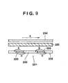
- FIG. 8 is a view taken along the arrowed line VIII-VIII of FIG. 7 .
- FIG. 9 is a view taken along the arrowed line IX-IX of FIG. 8 .
- the same members as the members illustrated in FIG. 2 are assigned the same numerals, and duplicate explanations are omitted.
- An upper surface of the chamber 201 is an opening, which is closed with a disk-shaped ceiling board 230 made of an insulating material (for example, a ceramic).
- An etched member 231 made of a metal (copper, Cu) is interposed between the opening at the upper surface of the chamber 201 and the ceiling board 230.
- the etched member 231 is provided with a ring portion 232 fitted to the opening at the upper surface of the chamber 201.
- a plurality of (12 in the illustrated embodiment) protrusions 233 which extend close to the center in the diametrical direction of the chamber 201 and have the same width, are provided in the circumferential direction on the inner periphery of the ring portion 232.
- the protrusions 233 are integrally or removably attached to the ring portion 232. Notches (spaces) 235 formed between the protrusions 233 are present between the ceiling board 230 and the interior of the chamber 201.
- the ring portion 232 is earthed, and the plural protrusions 233 are electrically connected together and maintained at the same potential.
- Temperature control means (not shown), such as a heater, is provided in the etched member 231 to control the temperature of the etched member 231 to 200 to 400°C, for example.
- Second protrusions shorter in the diametrical direction than the protrusions 233 can be arranged between the protrusions 233. Moreover, short protrusions can be arranged between the protrusion 233 and the second protrusion. By so doing, the area of copper, an object to be etched, can be secured, with an induced current being suppressed.
- the plasma antenna 234 is formed in a planar ring shape parallel to the surface of the ceiling board 230.
- a matching instrument 210 and a power source 211 are connected to the plasma antenna 234 to supply power.
- the etched member 231 has the plurality of protrusions 233 provided in the circumferential direction on the inner periphery of the ring portion 232, and includes the notches (spaces) 235 formed between the protrusions 233.
- the protrusions 233 are arranged between the substrate 203 and the ceiling board 230 in a discontinuous state relative to the flowing direction of electricity in the plasma antenna 234.
- the source gas is supplied through the nozzles 212 to the interior of the chamber 201, and electromagnetic waves are shot from the plasma antenna 234 into the chamber 201.
- the Cl 2 gas is ionized to generate a Cl 2 gas plasma (source gas plasma) 214.
- the etched member 231, an electric conductor, is present below the plasma antenna 234.
- the Cl 2 gas plasma 214 occurs stably between the etched member 231 and the substrate 203, namely, below the etched member 231, under the following action:
- the etched member 231 When the etched member 231 is viewed from the substrate 203, therefore, there is no flow in a direction in which the flow A of electricity in the plasma antenna 234 is canceled out. Furthermore, the ring portion 232 is earthed, and the protrusions 233 are maintained at the same potential. Thus, even though the etched member 231, an electric conductor, exists, the electromagnetic wave is reliably thrown from the plasma antenna 234 into the chamber 201. Consequently, the Cl 2 gas plasma 214 is stably generated below the etched member 231.
- the Cl 2 gas plasma 214 causes an etching reaction to the etched member 231 made of copper, forming a precursor (Cu x Cl y ) 215.
- the etched member 231 is maintained by the Cl 2 gas plasma 214 at a predetermined temperature (e.g., 200 to 400°C) which is higher than the temperature of the substrate 203.
- the precursor (Cu x Cl y ) 215 formed within the chamber 201 is transported toward the substrate 203 controlled to a lower temperature than the temperature of the etched member 231.
- the precursor (Cu x Cl y ) 215 transported toward the substrate 203 is converted into only Cu ions by a reduction reaction, and directed at the substrate 203 to form a thin Cu film 216 on the surface of the substrate 203.
- the reactions involved are the same as in the aforementioned fifteenth embodiment.
- the gases and the etching products, which have not been involved in the reactions, are exhausted through an exhaust port 217.
- the metal film production apparatus constructed as above uses the Cl 2 gas plasma (source gas plasma) 214, the reaction efficiency is markedly increased, and the speed of film formation is fast. Since the Cl 2 gas is used as the source gas, moreover, the cost can be markedly decreased. Furthermore, the substrate 203 is controlled to a lower temperature than the temperature of the etched member 231 by use of the temperature control means 206. Thus, the amounts of impurities, such as chlorine, remaining in the thin Cu film 216 can be decreased, so that a high quality thin Cu film 216 can be produced.
- the Cl 2 gas plasma source gas plasma
- the etched member 231 has the plurality of protrusions 233 provided in the circumferential direction on the inner periphery of the ring portion 232, and includes the notches (spaces) 235 formed between the protrusions 233.
- the induced currents generated in the etched member 231 flow in the same direction as the flowing direction of electricity in the plasma antenna 234, when viewed from the substrate 203. Therefore, even though the etched member 231, an electric conductor, exists below the plasma antenna 234, the electromagnetic waves are reliably thrown from the plasma antenna 234 into the chamber 201. Consequently, the Cl 2 , gas plasma 214 can be stably generated below the etched member 231.
- Diluent gas nozzles 221 are provided, as diluent gas supply means, for supplying an Ar gas, as a diluent gas, to the interior of the chamber 201 above the surface of the substrate 203.
- the Ar gas is supplied from the diluent gas nozzle 221, and electromagnetic waves are shot from the plasma antenna 234 into the chamber 201, whereby the Ar gas is ionized to generate an Ar gas plasma (surface treatment plasma generation means).
- a bias power source 220 is connected to the support platform 202, and a bias voltage is applied thereto for supporting the substrate 203 on the support platform 202.
- the barrier metal film 223 of TaN has been formed, as shown in FIG. 4 .
- the barriermetal film 223 on the surface of the substrate 203 is etched with Ar + to flatten the barrier metal film 223.
- denitrification is performed in which the nitrogen atoms (N) of the TaN in the superficial layer of the barrier metal film 223 are removed to decrease the nitrogen content of the superficial layer relative to the interior of the matrix of the barrier metal film 223.
- WN or TiN can also be applied.
- the flattening of the barrier metal film 223 and its denitrification upon generation of the Ar gas plasma are carried out before formation of the aforementioned thin Cu film 216.
- the details of the flattening of the barrier metal film 223, and the details of the denitrification of this film are the same as in the fifteenth embodiment, and relevant explanations are omitted.
- the barrier metal film 223 can be in a two-layer structure state without becoming thick, and yet the metal layer 223a can retain adhesion to the thin Cu film 216, while the TaN layer 223b can prevent diffusion of Cu. Consequently, the thin Cu film 216 can be formed, with satisfactory adhesion, without diffusion into the substrate 203, so that the Cu wiring process can be stabilized.
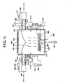
- FIG. 10 is a schematic side view of the metal film production apparatus according to the seventeenth embodiment of the present invention.
- the same members as the members illustrated in FIGS. 2 and 7 are assigned the same numerals, and duplicate explanations are omitted.
- the opening of an upper portion of a chamber 201 is closed with a ceiling board 230, for example, made of a ceramic (an insulating material).
- An etched member 241 made of a metal (copper, Cu) is provided on a lower surface of the ceiling board 230, and the etched member 241 is of a quadrangular pyramidal shape.
- Slit-shaped opening portions 242 are formed at a plurality of locations (for example, four locations) in the periphery of an upper part of the cylindrical portion of the chamber 201, and one end of a tubular passage 243 is fixed to each of the opening portions 242.
- a tubular excitation chamber 244 made of an insulator is provided halfway through the passage 243, and a coiled plasma antenna 245 is provided around the excitation chamber 244.
- the plasma antenna 245 is connected to a matching instrument 248 and a power source 249 to receive power.
- the plasma antenna 2 4 5 , the matching instrument 248 and the power source 249 constitute plasma generation means.
- a flow controller 246 is connected to the other end of the passage 243, and a chlorine-containing source gas (a Cl 2 gas diluted with He or Ar to a chlorine concentration of ⁇ 50%, preferably about 10%) is supplied into the passage 243 via the flow controller 246.
- a chlorine-containing source gas a Cl 2 gas diluted with He or Ar to a chlorine concentration of ⁇ 50%, preferably about 10%
- the Cl 2 gas is ionized to generate a Cl 2 gas plasma (source gas plasma) 247. Because of the generation of the Cl 2 gas plasma 247, excited chlorine is fed into the chamber 201 through the opening portion 42, whereupon the etched member 241 is etched with excited chlorine.
- the source gas is supplied into the passage 243 via the flow controller 246 and fed into the excitation chamber 244.
- the Cl 2 gas is ionized to generate a Cl 2 gas plasma (source gas plasma) 247. Since a predetermined differential pressure has been established between the pressure inside the chamber 201 and the pressure inside the excitation chamber 244 by the vacuum device 208, the excited chlorine of the Cl 2 gas plasma 247 in the excitation chamber 244 is fed to the etched member 241 inside the chamber 201 through the opening portion 242.
- the excited chlorine causes an etching reaction to the etched member 241, forming a precursor (M x Cl y ) 215 inside the chamber 201.
- the etched member 241 is maintained at a predetermined temperature (e.g. , 200 to 400°C), which is higher than the temperature of the substrate 203, by a heater 250.
- the precursor (Cu x Cl y ) 215 formed inside the chamber 201 is transported toward the substrate 203 controlled to a lower temperature than the temperature of the etched member 241.
- the precursor (Cu x Cl y ) 215 transported toward the substrate 203 is converted into only Cu ions by a reduction reaction, and directed at the substrate 203 to form a thin Cu film 216 on the surface of the substrate 203.
- the reactions on this occasion are the same as in the aforementioned fifteenth embodiment, and the gases and etching products that have not been involved in the reactions are exhausted through an exhaust port 217.
- the Cl 2 gas plasma 247 is generated in the excitation chamber 244 isolated from the chamber 201.
- the substrate 203 is not exposed to the plasma any more, and the substrate 203 becomes free from damage from the plasma.
- the means for generating the Cl 2 gas plasma 247 in the excitation chamber 244 it is possible to use microwaves, laser, electron rays, or synchrotron radiation. It is also permissible to form the precursor by heating a metal filament to a high temperature.
- the construction for isolating the Cl 2 gas plasma 247 from the substrate 203 may be the provision of the excitation chamber 244 in the passage 243, or may be other construction, for example, the isolation of the chamber 201.
- the above-described metal film production apparatus is provided with diluent gas nozzles 221, as diluent gas supply means, for supplying an Ar gas, as a diluent gas, to the interior of the chamber 201 above the surface of the substrate 203.
- a coil-shaped surface treatment plasma antenna 236 is provided on a trunk portion of the chamber 201.
- a matching instrument 237 and a power source 238 are connected to the surface treatment plasma antenna 236 to supply power.
- the Ar gas is supplied from the diluent gas nozzles 221, and electromagnetic waves are shot from the plasma antenna 236 into the chamber 201, whereby the Ar gas is ionized to generate an Ar gas plasma (surface treatment plasma generation means).
- a bias power source 220 is connected to the support platform 202, and a bias voltage is applied thereto for supporting the substrate 203 on the support platform 202.
- a barrier metal film 223 of TaN has been formed, as shown in FIG. 31.
- the barrier metal film 223 on the surface of the substrate 203 is etched with Ar + to flatten the barrier metal film 223.
- denitrification is performed in which the nitrogen atoms (N) of the TaN in the superficial layer of the barrier metal film 223 are removed to decrease the nitrogen content of the superficial layer relative to the interior of the matrix of the barrier metal film 223.
- the barrier metal film 223, WN or TiN can also be applied.
- the flattening of the barrier metal film 223 and its denitrification upon generation of the Ar gas plasma are carried out before formation of the aforementioned thin Cu film 216.
- the details of the flattening of the barrier metal film 223 and the denitrification of this film are the same as in the previous example ( Fig 2 ), and relevant explanations are omitted.
- the barrier metal film 223 can be in a two-layer structure state without becoming thick, and yet the metal layer 223a (see FIG. 6 ) can retain adhesion to the thin Cu film 216, while the TaN layer 223b (see FIG. 6 ) can prevent diffusion of Cu. Consequently, the thin Cu film 216 can be formed, with satisfactory adhesion, without diffusion into the substrate 203, so that the Cu wiring process can be stabilized.
- FIG. 11 is a schematic side view of the metal film production apparatus according to the eighteenth embodiment of the present invention.
- the same members as the members illustrated in FIGS. 2 , 7 and 10 are assigned the same numerals, and duplicate explanations are omitted.
- the plasma antenna 209 is not provided around the cylindrical portion of the chamber 201, and the matching instrument 210 and power source 211 are connected to the copper plate member 207 for supply of power to the copper plate member 207.
- the source gas is supplied from the nozzles 212 into the chamber 201, and electromagnetic waves are shot from the copper plate member 207 into the chamber 201, the Cl 2 gas is ionized to generate a Cl 2 gas plasma (source gas plasma) 214.
- the Cl 2 gas plasma 214 causes an etching reaction to the copper plate member 207, forming a precursor (Cu x Cl y ) 215.
- the copper plate member 207 is maintained at a predetermined temperature (e.g., 200 to 400°C), which is higher than the temperature of the substrate 203, by the Cl 2 gas plasma 214.
- the precursor (Cu x Cl y ) 215 formed inside the chamber 201 is transported toward the substrate 203 controlled to a lower temperature than the temperature of the copper plate member 207.
- the precursor (Cu x Cl y ) 215 transported toward the substrate 203 is converted into only Cu ions by a reduction reaction, and directed at the substrate 203 to form a thin Cu film 216 on the surface of the substrate 203.
- the reactions on this occasion are the same as in the aforementioned fifteenth embodiment, and the gases and etching products that have not been involved in the reactions are exhausted through an exhaust port 217.
- the copper plate member 207 itself is applied as an electrode for plasma generation.
- the plasma antenna 209 intended to prepare the thin Cu film 216 need not be provided around the cylindrical portion of the chamber 201.
- the above-described metal film production apparatus is provided with diluent gas nozzles 221, as diluent gas supply means, for supplying an Ar gas, as a diluent gas, to the interior of the chamber 201 above the surface of the substrate 203.
- Supply of the source gas through the nozzles 212 is cut off, the Ar gas is supplied from the diluent gas nozzles 221, and electromagnetic waves are shot from the copper plate member 207 into the chamber 201.
- the Ar gas is ionized to generate an Ar gas plasma (surface treatment plasma generation means).
- a bias power source 220 is connected to the support platform 202, and a bias voltage is applied thereto for supporting the substrate 203 on the support platform 202.
- a barrier metal film 223 of TaN has been formed, as shown in FIG. 4 .
- the barrier metal film 223 on the surface of the substrate 203 is etched with Ar + to flatten the barrier metal film 223.
- denitrification is performed in which the nitrogen atoms (N) of the TaN in the superficial layer of the barrier metal film 223 are removed to decrease the nitrogen content of the superficial layer relative to the interior of the matrix of the barrier metal film 223.
- the barrier metal film 223, WN or TiN can also be applied.
- the surface treatment plasma generation means it is permissible to provide a coiled surface treatment plasma antenna on the trunk portion of the chamber 201, and supply power via a matching instrument and a power source, thereby generating an Ar gas plasma.
- the flattening of the barrier metal film 223 and its denitrification upon generation of the Ar gas plasma are carried out before formation of the aforementioned thin Cu film 216.
- the details of the flattening of the barrier metal film 223 and the denitrification of this film are the same as in the previous example ( Fig. 2 ), and relevant explanations are omitted.
- the barrier metal film 223 can be in a two-layer structure state without becoming thick, and the metal layer 223a (see FIG. 6 ) can retain adhesion to the thin Cu film 216, while the TaN layer 223b (see FIG. 33) can prevent diffusion of Cu. Consequently, the thin Cu film 216 can be formed, with satisfactory adhesion, without diffusion into the substrate 203, so that the Cu wiring process can be stabilized.
- FIG. 12 schematically shows a side view of the metal film production apparatus according to the nineteenth embodiment of the present invention.
- a support platform 252 is provided near the bottom of a cylindrical chamber 251 made of, say, a ceramic (an insulating material), and a substrate 253 is placed on the support platform 252.
- Temperature control means 256 equipped with a heater 254 and refrigerant flow-through means 255 is provided in the support platform 252 so that the support platform 252 is controlled to a predetermined temperature (for example, a temperature at which the substrate 253 is maintained at 100 to 200°C) by the temperature control means 256.
- An upper surface of the chamber 251 is an opening, which is closed with a metal member 257, as an etched member, made of a metal (e.g., W, Ti, Ta, or TiSi).
- a metal member 257 as an etched member, made of a metal (e.g., W, Ti, Ta, or TiSi).
- the interior of the chamber 251 closed with the metal member 257 is maintained at a predetermined pressure by a vacuum device 258.
- a plasma antenna 259 as a coiled winding antenna of plasma generation means, is provided around a cylindrical portion of the chamber 251.
- a matching instrument 260 and a power source 261 are connected to the plasma antenna 259 to supply power.
- Nozzles 262 for supplying a source gas (a Cl 2 gas diluted with He or Ar to a chlorine concentration of ⁇ 50%, preferably about 10%), containing chlorine as a halogen, to the interior of the chamber 251 are connected to the cylindrical portion of the chamber 251 below the metal member 257.
- the nozzle 262 is open toward the horizontal, and is fed with the source gas via a flow controller 263 (halogen gas supply means).
- Fluorine (F), bromine (Br) or iodine (I) can also be applied as the halogen to be incorporated into the source gas.
- Slit-shaped opening portions 264 are formed at a plurality of locations (for example, four locations) in the periphery of a lower part of the cylindrical portion of the chamber 251, and one end of a tubular passage 265 is fixed to each of the opening portions 264.
- a tubular excitation chamber 266 made of an insulator is provided halfway through the passage 265, and a coiled plasma antenna 267 is provided around the excitation chamber 266.
- the plasma antenna 267 is connected to a matching instrument 268 and a power source 269 to receive power.
- the plasma antenna 267, the matching instrument 268 and the power source 269 constitute excitation means.
- a flow controller 270 is connected to the other end of the passage 265, and an ammonia gas (NH 3 gas) as a nitrogen-containing gas is supplied into the passage 265 via the flow controller 270.
- NH 3 gas ammonia gas
- the source gas is supplied through the nozzles 262 to the interior of the chamber 251, and electromagnetic waves are shot from the plasma antenna 259 into the chamber 251.
- the Cl 2 gas is ionized to generate a Cl 2 gas plasma (source gas plasma) 271.
- the Cl 2 gas plasma 271 causes an etching reaction to the metal member 257, forming a precursor (M x Cl y : M is a metal such as W, Ti, Ta or TiSi) 272.
- the NH 3 gas is supplied into the passage 265 via the flow controller 270 and fed into the excitation chamber 266.
- the NH 3 gas is ionized to generate an NH 3 gas plasma 263. Since a predetermined differential pressure has been established between the pressure inside the chamber 251 and the pressure inside the excitation chamber 266 by the vacuum device 258, the excited ammonia of the NH 3 gas plasma 273 in the excitation chamber 266 is fed to the precursor (M x Cl y ) 272 inside the chamber 251 through the opening portion 264.
- excitation means for exciting the nitrogen-containing gas in the excitation chamber 266 isolated from the chamber 251 is constructed. Because of this construction, the metal component of the precursor (M x Cl y ) 272 and ammonia react to form a metal nitride (MN) (formation means). At this time, the metal member 257 and the excitation chamber 266 are maintained by the plasmas at predetermined temperatures (e.g., 200 to 400°C) which are higher than the temperature of the substrate 253.
- predetermined temperatures e.g. 200 to 400°C
- the metal nitride (MN) formed within the chamber 251 is transported toward the substrate 253 controlled to a low temperature, whereby a thin MN film 274 (a TaN film if the metal member 257 of Ta is applied) is formed on the surface of the substrate 253.
- MN metal nitride
- the reaction for formation of the thin MN film 274 can be expressed by: 2MCl + 2NH 3 ⁇ 2MN ⁇ + HCl ⁇ + + 2H 2 ⁇
- the gases and the etching products that have not been involved in the reactions are exhausted through an exhaust port 277.
- the source gas has been described, with the Cl 2 gas diluted with, say, He or Ar taken as an example.
- the Cl 2 gas can be used alone, or an HCl gas can also be applied.
- an HCl gas plasma is generated as the source gas plasma.
- the source gas may be any gas containing chlorine, and a gas mixture of an HCl gas and a Cl 2 gas is also usable.
- the material for the metal member 257 it is possible to use an industrially applicable metal such as Ag, Au, Pt or Si.
- the NH 3 gas is supplied into the passage 265 and fed into the excitation chamber 266.
- an NH 3 gas plasma can be generated within the chamber 251 by supplying an NH 3 gas into the chamber 251 and supplying power to the plasma antenna 259.
- the chamber 265, excitation chamber 266, plasma antenna 267, matching instrument 268 and power source 269 can be omitted.
- the metal is formed by plasmas to produce the thin MN film 274 as the barrier metal film.
- the barrier metal film can be formed uniformly to a small thickness. Consequently, the barrier metal film can be formed highly accurately at a high speed with excellent burial properties in a very small thickness even to the interior of a tiny depression, for example, several hundred nanometers wide, which has been provided in the substrate 253.
- the above-described metal film production apparatus is provided with diluent gas nozzles 276, as diluent gas supply means, for supplying an Ar gas, as a diluent gas, to the interior of the chamber 251 above the surface of the substrate 253.
- the Ar gas is supplied from the diluent gas nozzles 276, and electromagnetic waves are shot from the plasma antenna 259 into the chamber 251, whereby the Ar gas is ionized to generate an Ar gas plasma (surface treatment plasma generation means).
- a bias power source 277 is connected to the support platform 252, and a bias voltage is applied thereto for supporting the substrate 253 on the support platform 252.
- the thin MN film 274 as a barrier metal film is formed, whereafter an Ar gas plasma is generated.
- the barrier metal film on the surface of the substrate 253 is etched with Ar + to flatten the barrier metal film.
- denitrification is performed in which the nitrogen atoms (N) of the TaN in the superficial layer of the barrier metal film are removed.
- a thin copper (Cu) film or a thin aluminum (Al) film is formed on the barrier metal film by a film forming device.
- the details of the flattening of the barrier metal film and the denitrification of this film upon generation of the Ar gas plasma are the same as in the fifteenth embodiment. Thus, relevant explanations are omitted.
- the barrier metal film can be in a two-layer structure state without becoming thick, and the resulting metal layer can retain adhesion to a thin metal film formed by film formation in the subsequent step.
- the TaN layer can prevent diffusion of metal during film formation in the subsequent step. Consequently, the thin metal film (thin Cu film) during film formation in the subsequent step can be formed, with satisfactory adhesion, without diffusion into the substrate 253, so that the Cu wiring process can be stabilized.
- the construction of the metal film production apparatus for producing the barrier metal film may employ a device of the type generating a capacitive coupling plasma, or a device of the remote type which generates a plasma in a manner isolated from a film formation chamber.
- a barrier metal film of TaN is subjected to a treatment for etching the surface and forming nuclei of silicon atoms by use of a plasma of a silicon-containing gas (for example, silane, SiH 4 , a hydride of silicon).
- a silicon-containing gas for example, silane, SiH 4 , a hydride of silicon.
- Silicon which is not a foreign matter, has good adhesion to a metal, and the formation of nuclei of silicon atoms on the surface can increase adhesion between the metal of a barrier metal film and a metal to be formed as a film thereon.
- a disilane (Si 2 H 6 ) gas or a trisilane (Si 3 H 6 ) can be used in addition to the SiH 4 gas.
- an SiCl 4 gas, an SiH 2 Cl 2 gas or an SiHCl 3 gas can be applied. Any such gas may be diluted with a diluent gas and supplied.
- a concrete apparatus construction according to the third aspect of the invention may be as follows: Using a barrier metal film production apparatus, a source gas containing a halogen (e.g., a chlorine-containing gas) is supplied to the interior of a chamber between a substrate and an etched member of Ta, and an atmosphere within the chamber is converted into a plasma to generate a chlorine gas plasma.
- the etched member is etched with the chlorine gas plasma to form a precursor comprising the Ta component contained in the etched member and the chlorine gas.
- a nitrogen-containing gas is excited, and TaN, a metal nitride, is formed upon reaction between the excited nitrogen and the precursor.
- the resulting TaN is formed as a film on the substrate kept at a low temperature to form a barrier metal film.
- an SiH 4 gas plasma a gas containing silicon, is generated within the chamber to form crystal grains of Si. That is, a barrier metal film production apparatus shown, for example, in FIG. 12 can be applied.
- a concrete apparatus construction according to the invention may be as follows: A chlorine gas is supplied into the chamber, and an atmosphere within the chamber is converted into a plasma to generate a chlorine gas plasma. An etched member made of copper (Cu) is etched with the chlorine gas plasma to form a precursor comprising the Cu component contained in the etched member and chlorine inside the chamber. The temperature of the substrate is rendered lower than the temperature of the etched member to form a film of the Cu component of the precursor on the substrate. This process is performed using a metal film forming device. The substrate having a barrier metal film of TaN formed thereon is housed in the chamber.
- Cu copper
- an SiH 4 gas plasma a plasma of a silicon-containing gas, is generated within the chamber to form crystal grains of Si. That is, the metal film production apparatus shown, for example, in FIG. 2 , 7 , 10 or 11 can be applied.
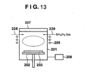
- FIG. 13 shows the conceptual construction of a metal film production apparatus according to the twenty-first embodiment of the present invention.
- FIG. 14 shows the concept status of a barrier metal film in the formation of nuclei of Si.
- the illustrated metal film production apparatus has the conceptual construction of the metal film production apparatus according to the example shown in FIG. 2 , in which the gas supplied through the nozzles 21 is made different. Thus, the formation of the thin Cu film in the metal film production apparatus is the same, and its explanation is omitted hereinbelow.
- silicon-containing gas nozzles 228 are provided, as silicon-containing gas supply means, for supplying a silane gas (SiH 4 gas), as a gas containing silicon, to the interior of a chamber 201 above the surface of a substrate 203.
- a silane gas SiH 4 gas
- An SiH 4 gas diluted with hydrogen is supplied through the silicon-containing gas nozzles 228, and electromagnetic waves are shot from a plasma antenna 209 into the chamber 201, whereby the hydrogen-diluted SiH 4 gas is ionized to generate an SiH 4 gas plasma (surface treatment plasma means).
- a barrier metal film 223 of TaN (see FIG. 4 ) has been formed.
- Generation of the SiH 4 gas plasma results in the growth of crystal grains of Si and the appearance of H 2 . While film formation is proceeding, crystal grains of Si are formed as nuclei on the superficial layer of the substrate 203 by the etching action of H 2 .
- the formation of the nuclei of Si upon generation of the SiH 4 gas plasma is performed before formation of the thin Cu film 216 explained in the example of FIG. 2 . That is, when the substrate 203 having the barrier metal film 223 of TaN (see FIG. 4 ) formed there on is admitted onto the support platform 202, a hydrogen-diluted SiH 4 gas is supplied through the silicon-containing gas nozzles 228 prior to the formation of the thin Cu film 216 (see FIG. 2 ). Also, electromagnetic waves are shot from the plasma antenna 209 into the chamber 201 to generate an SiH 4 gas plasma.
- the ratio of SiH 4 to hydrogen in the hydrogen-diluted SiH 4 gas is set, for example, as follows: SiH 4/ hydrogen ⁇ 5/100.
- argon, helium, neon or other diluent gas can be applied in addition to hydrogen.
- the SiH 4 gas plasma is generated, the reaction SiH 4 ⁇ Si + H 2 proceeds.
- crystal grains of Si are formed as nuclei on the superficial layer of the barrier metal film 223 by the etching action of H 2 , as shown in FIG. 14 .
- the sizes of the nuclei of Si can be controlled appropriately by controlling the conditions for the plasma, the ratio of hydrogen dilution, the flow rate of the gas, etc.
- the etching action of H 2 removes the nitrogen atoms (N) of the barrier metal film 223, and can bring the state of the barrier metal film 223 having a two-layer structure, a metal layer 223a substantially composed of Ta (see FIG. 6 ), and a TaN layer 223b (see FIG. 6 ).
- the SiH 4 gas is diluted with hydrogen, the crystallinity of Si can be improved, and its nuclei are easy to form.
- Silicon, which is not a foreign matter, has good adhesion to Ta and Cu, and the formation of nuclei of Si on the surface of the barrier metal film 223 can increase adhesion between Ta of the barrier metal film 223 and Cu to be formed as a film thereon.
- a barrier metal film 223 preventing diffusion of the metal and retaining adhesion to the metal is produced with good efficiency and without deterioration of performance.
- the SiH 4 gas plasma is generated within the chamber 201 accommodating the substrate 203 having the barrier metal film 223 formed thereon, whereby crystal grains of Si are formed as nuclei on the superficial layer of the barrier metal film 223.
- adhesion to Ta and Cu can be improved. Consequently, the barrier metal film 223 can be formed with satisfactory adhesion and anti-diffusion properties without becoming thick, so that the Cu wiring process can be stabilized.
- the embodiment described above can be applied to the metal film production apparatuses of the examples shown in FIGS. 7 , 10 and 11 . It is also applicable to the barrier metal film production apparatus of the nineteenth embodiment shown in FIG. 12 . It is also possible to combine the flattening of the surface with Ar + upon generation of the Ar gas plasma in the pervious embodiments with the formation of crystal grains of Si as nuclei on the superficial layer of the barrier metal film 223. In this case, a common nozzle can be used by diluting an SiH 4 gas with an Ar gas, and the flattening of the surface and the formation of Si nuclei can be easily switched by controlling the flow rate of the Ar gas.
Landscapes
- Chemical & Material Sciences (AREA)
- Engineering & Computer Science (AREA)
- Materials Engineering (AREA)
- Organic Chemistry (AREA)
- Metallurgy (AREA)
- Mechanical Engineering (AREA)
- General Chemical & Material Sciences (AREA)
- Chemical Kinetics & Catalysis (AREA)
- Inorganic Chemistry (AREA)
- Physics & Mathematics (AREA)
- Plasma & Fusion (AREA)
- Electrochemistry (AREA)
- Chemical Vapour Deposition (AREA)
- Electrodes Of Semiconductors (AREA)
- Internal Circuitry In Semiconductor Integrated Circuit Devices (AREA)
- Physical Vapour Deposition (AREA)
Claims (4)
- System zur Herstellung einer Metallschicht, umfassend:eine Kammer (201) zur Aufnahme eines Substrats (203), das eine Barrieremetallschicht (223) eines Metallnitrids aufweist, das darauf gebildet wird;einen Silizium enthaltenden Gaszuführungsstutzen (228), um ein Silizium enthaltendes Gas einer Stelle oberhalb einer Oberfläche des Substrats (203) zuzuführen;Plasmaerzeugungsmittel (209) zum Erzeugen von Silizium enthaltendes Gasplasma, um Kerne von Siliziumatomen auf einer Oberfläche der Barrieremetallschicht auf der Oberfläche des Substrats zu bilden;ein geätztes metallisches Element(207), das in der Kammer bereitgestellt wird;ein Quellgaszuführungsstutzen (212), um dem Inneren der Kammer - zwischen dem Substrat und dem geätzten Element - ein Quellgas, das ein Halogen enthält, zuzuführen;
wobei das Plasmaerzeugungsmittel (209) ferner dafür eingerichtet ist, um das Quellgas, das das Halogen enthält, in ein Plasma umzuwandeln, um ein Quellgasplasma zu erzeugen, sodass das geätzte Element mit dem Quellgasplasma geätzt wird, um eine Vorläuferverbindung aus einer in dem geätzten Element enthaltenen Metallkomponente und dem Quellgas zu bilden; undSteuerungsmittel, um dafür zu sorgen, dass die Temperatur des Substrats niedriger als die Temperatur des geätzten Elements ist, um die Metallkomponente der Vorläuferverbindung als eine Schicht auf der Barrieremetallschicht zu bilden, die die Kerne von Siliziumatomen, die auf deren Oberfläche gebildet werden, aufweist. - System nach Anspruch 1, wobei das Silizium enthaltende Gas ein Silan ist.
- System nach einem der Patentansprüche 1 oder 2,
wobei das Metallnitrid ein Tantalnitrid, Wolframnitrid oder Titannitrid ist. - System nach einem der Patentansprüche 1 bis 3, wobei das Steuerungsmittel (206) einen Erhitzer (204) und/oder ein Mittel zum Durchströmen von Kühlmittel (205) umfasst.
Applications Claiming Priority (9)
| Application Number | Priority Date | Filing Date | Title |
|---|---|---|---|
| JP2001348325 | 2001-11-14 | ||
| JP2001348325 | 2001-11-14 | ||
| JP2002027738A JP4589591B2 (ja) | 2002-02-05 | 2002-02-05 | 金属膜作製方法及び金属膜作製装置 |
| JP2002027738 | 2002-02-05 | ||
| JP2002044296A JP3649697B2 (ja) | 2001-11-14 | 2002-02-21 | バリアメタル膜作製装置及びバリアメタル膜作製方法 |
| JP2002044289A JP3665031B2 (ja) | 2002-02-21 | 2002-02-21 | バリアメタル膜作製装置及びバリアメタル膜作製方法 |
| JP2002044289 | 2002-02-21 | ||
| JP2002044296 | 2002-02-21 | ||
| EP02024416A EP1312696A3 (de) | 2001-11-14 | 2002-10-28 | Vorrichtung und Methode zur Herstellung von Barriereschichten für Metalle sowie Vorrichtung und Methode zur Herstellung von Metallschichten |
Related Parent Applications (1)
| Application Number | Title | Priority Date | Filing Date |
|---|---|---|---|
| EP02024416A Division EP1312696A3 (de) | 2001-11-14 | 2002-10-28 | Vorrichtung und Methode zur Herstellung von Barriereschichten für Metalle sowie Vorrichtung und Methode zur Herstellung von Metallschichten |
Publications (4)
| Publication Number | Publication Date |
|---|---|
| EP1473379A2 EP1473379A2 (de) | 2004-11-03 |
| EP1473379A8 EP1473379A8 (de) | 2005-02-23 |
| EP1473379A3 EP1473379A3 (de) | 2006-01-11 |
| EP1473379B1 true EP1473379B1 (de) | 2009-08-05 |
Family
ID=27482680
Family Applications (8)
| Application Number | Title | Priority Date | Filing Date |
|---|---|---|---|
| EP04017491A Expired - Lifetime EP1473379B1 (de) | 2001-11-14 | 2002-10-28 | Vorrichtung und Verfahren zur Herstellung von Metallschichten |
| EP04017493A Expired - Lifetime EP1475454B1 (de) | 2001-11-14 | 2002-10-28 | Vorrichtung und Methode zur Herstellung von Barriereschichten für Metalle sowie Vorrichtung und Methode zur Herstellung von Metallschichten |
| EP04017496A Expired - Lifetime EP1475457B1 (de) | 2001-11-14 | 2002-10-28 | Vorrichtung und Methode zur Herstellung von Barriereschichten für Metalle sowie Vorrichtung und Methode zur Herstellung von Metallschichten |
| EP04017497A Withdrawn EP1473380A3 (de) | 2001-11-14 | 2002-10-28 | Vorrichtung und Methode zur Herstellung von Metallschichten |
| EP04017492A Withdrawn EP1475453A3 (de) | 2001-11-14 | 2002-10-28 | Vorrichtung und Verfahren zur Herstellung von Metallschichten |
| EP04017495A Expired - Lifetime EP1475456B1 (de) | 2001-11-14 | 2002-10-28 | Vorrichtung und Verfahren zur Herstellung von Barriereschichten für Metalle sowie Vorrichtung und Verfahren zur Herstellung von Metallschichten |
| EP02024416A Ceased EP1312696A3 (de) | 2001-11-14 | 2002-10-28 | Vorrichtung und Methode zur Herstellung von Barriereschichten für Metalle sowie Vorrichtung und Methode zur Herstellung von Metallschichten |
| EP04017494A Withdrawn EP1475455A3 (de) | 2001-11-14 | 2002-10-28 | Vorrichtung und Methode zur Herstellung von Barriereschichten für Metalle sowie Vorrichtung und Methode zur Herstellung von Metallschichten |
Family Applications After (7)
| Application Number | Title | Priority Date | Filing Date |
|---|---|---|---|
| EP04017493A Expired - Lifetime EP1475454B1 (de) | 2001-11-14 | 2002-10-28 | Vorrichtung und Methode zur Herstellung von Barriereschichten für Metalle sowie Vorrichtung und Methode zur Herstellung von Metallschichten |
| EP04017496A Expired - Lifetime EP1475457B1 (de) | 2001-11-14 | 2002-10-28 | Vorrichtung und Methode zur Herstellung von Barriereschichten für Metalle sowie Vorrichtung und Methode zur Herstellung von Metallschichten |
| EP04017497A Withdrawn EP1473380A3 (de) | 2001-11-14 | 2002-10-28 | Vorrichtung und Methode zur Herstellung von Metallschichten |
| EP04017492A Withdrawn EP1475453A3 (de) | 2001-11-14 | 2002-10-28 | Vorrichtung und Verfahren zur Herstellung von Metallschichten |
| EP04017495A Expired - Lifetime EP1475456B1 (de) | 2001-11-14 | 2002-10-28 | Vorrichtung und Verfahren zur Herstellung von Barriereschichten für Metalle sowie Vorrichtung und Verfahren zur Herstellung von Metallschichten |
| EP02024416A Ceased EP1312696A3 (de) | 2001-11-14 | 2002-10-28 | Vorrichtung und Methode zur Herstellung von Barriereschichten für Metalle sowie Vorrichtung und Methode zur Herstellung von Metallschichten |
| EP04017494A Withdrawn EP1475455A3 (de) | 2001-11-14 | 2002-10-28 | Vorrichtung und Methode zur Herstellung von Barriereschichten für Metalle sowie Vorrichtung und Methode zur Herstellung von Metallschichten |
Country Status (5)
| Country | Link |
|---|---|
| US (7) | US20030091739A1 (de) |
| EP (8) | EP1473379B1 (de) |
| KR (4) | KR100537320B1 (de) |
| DE (4) | DE60232823D1 (de) |
| TW (1) | TWI253478B (de) |
Families Citing this family (61)
| Publication number | Priority date | Publication date | Assignee | Title |
|---|---|---|---|---|
| US6951804B2 (en) * | 2001-02-02 | 2005-10-04 | Applied Materials, Inc. | Formation of a tantalum-nitride layer |
| US9076843B2 (en) | 2001-05-22 | 2015-07-07 | Novellus Systems, Inc. | Method for producing ultra-thin tungsten layers with improved step coverage |
| US20030145790A1 (en) * | 2002-02-05 | 2003-08-07 | Hitoshi Sakamoto | Metal film production apparatus and metal film production method |
| EP2050839A3 (de) | 2002-03-08 | 2009-05-13 | Canon Anelva Corporation | Verfahren und Vorrichtung zum Herstellen von Metall-Schichten |
| US6860944B2 (en) | 2003-06-16 | 2005-03-01 | Blue29 Llc | Microelectronic fabrication system components and method for processing a wafer using such components |
| WO2004114386A2 (en) * | 2003-06-16 | 2004-12-29 | Blue29 Corporation | Methods and system for processing a microelectronic topography |
| US6881437B2 (en) | 2003-06-16 | 2005-04-19 | Blue29 Llc | Methods and system for processing a microelectronic topography |
| US7883739B2 (en) | 2003-06-16 | 2011-02-08 | Lam Research Corporation | Method for strengthening adhesion between dielectric layers formed adjacent to metal layers |
| US20050277292A1 (en) * | 2004-05-28 | 2005-12-15 | Chao-Hsien Peng | Method for fabricating low resistivity barrier for copper interconnect |
| KR100607409B1 (ko) * | 2004-08-23 | 2006-08-02 | 삼성전자주식회사 | 기판 식각 방법 및 이를 이용한 반도체 장치 제조 방법 |
| US8158197B2 (en) * | 2005-03-03 | 2012-04-17 | Ulvac, Inc. | Method for forming tantalum nitride film |
| JP4931171B2 (ja) * | 2005-03-03 | 2012-05-16 | 株式会社アルバック | タンタル窒化物膜の形成方法 |
| JP4845455B2 (ja) * | 2005-09-01 | 2011-12-28 | キヤノンアネルバ株式会社 | 薄膜作製装置及び薄膜作製方法 |
| KR100738210B1 (ko) * | 2005-12-29 | 2007-07-10 | 동부일렉트로닉스 주식회사 | 반도체 장치의 박막 및 금속 배선 형성 방법 |
| CN101426952A (zh) * | 2006-04-18 | 2009-05-06 | 株式会社爱发科 | 成膜装置及阻挡膜的制造方法 |
| JP5297048B2 (ja) * | 2008-01-28 | 2013-09-25 | 三菱重工業株式会社 | プラズマ処理方法及びプラズマ処理装置 |
| JP4636133B2 (ja) | 2008-07-22 | 2011-02-23 | 東京エレクトロン株式会社 | 窒化チタン膜の改質方法及び改質装置 |
| US8551885B2 (en) * | 2008-08-29 | 2013-10-08 | Novellus Systems, Inc. | Method for reducing tungsten roughness and improving reflectivity |
| US9159571B2 (en) | 2009-04-16 | 2015-10-13 | Lam Research Corporation | Tungsten deposition process using germanium-containing reducing agent |
| US20100267230A1 (en) * | 2009-04-16 | 2010-10-21 | Anand Chandrashekar | Method for forming tungsten contacts and interconnects with small critical dimensions |
| US12444651B2 (en) | 2009-08-04 | 2025-10-14 | Novellus Systems, Inc. | Tungsten feature fill with nucleation inhibition |
| US10256142B2 (en) | 2009-08-04 | 2019-04-09 | Novellus Systems, Inc. | Tungsten feature fill with nucleation inhibition |
| US8709948B2 (en) * | 2010-03-12 | 2014-04-29 | Novellus Systems, Inc. | Tungsten barrier and seed for copper filled TSV |
| KR20120008360A (ko) * | 2010-07-16 | 2012-01-30 | 삼성모바일디스플레이주식회사 | 플렉서블 디스플레이용 기판 및 그 제조 방법 |
| KR101131891B1 (ko) * | 2010-07-30 | 2012-04-03 | 주식회사 하이닉스반도체 | 매립게이트를 구비한 반도체 장치 제조방법 |
| JP5544343B2 (ja) * | 2010-10-29 | 2014-07-09 | 東京エレクトロン株式会社 | 成膜装置 |
| CN102061442A (zh) * | 2011-01-27 | 2011-05-18 | 御林汽配(昆山)有限公司 | 在铝合金轮毂表面镀多层金属质感的工艺方法 |
| EP2559806A1 (de) | 2011-08-17 | 2013-02-20 | Center of Excellence Polymer Materials and Technologies (Polimat) | Verfahren zum Steigern der Hydrophilie polymerer Materialien |
| CN113862634A (zh) | 2012-03-27 | 2021-12-31 | 诺发系统公司 | 钨特征填充 |
| US9034760B2 (en) | 2012-06-29 | 2015-05-19 | Novellus Systems, Inc. | Methods of forming tensile tungsten films and compressive tungsten films |
| US8975184B2 (en) | 2012-07-27 | 2015-03-10 | Novellus Systems, Inc. | Methods of improving tungsten contact resistance in small critical dimension features |
| US8853080B2 (en) | 2012-09-09 | 2014-10-07 | Novellus Systems, Inc. | Method for depositing tungsten film with low roughness and low resistivity |
| US9153486B2 (en) | 2013-04-12 | 2015-10-06 | Lam Research Corporation | CVD based metal/semiconductor OHMIC contact for high volume manufacturing applications |
| KR101862632B1 (ko) | 2013-09-25 | 2018-05-31 | 캐논 아네르바 가부시키가이샤 | 자기 저항 효과 소자의 제조 방법 및 제조 시스템 |
| US9589808B2 (en) | 2013-12-19 | 2017-03-07 | Lam Research Corporation | Method for depositing extremely low resistivity tungsten |
| AU2015274511B2 (en) | 2014-06-11 | 2019-08-15 | Outdoor Wireless Networks LLC | Bitrate efficient transport through distributed antenna systems |
| US9997405B2 (en) | 2014-09-30 | 2018-06-12 | Lam Research Corporation | Feature fill with nucleation inhibition |
| US20160097118A1 (en) * | 2014-10-01 | 2016-04-07 | Seagate Technology Llc | Inductively Coupled Plasma Enhanced Chemical Vapor Deposition |
| US9953984B2 (en) | 2015-02-11 | 2018-04-24 | Lam Research Corporation | Tungsten for wordline applications |
| US9613818B2 (en) | 2015-05-27 | 2017-04-04 | Lam Research Corporation | Deposition of low fluorine tungsten by sequential CVD process |
| US9754824B2 (en) | 2015-05-27 | 2017-09-05 | Lam Research Corporation | Tungsten films having low fluorine content |
| US9978605B2 (en) | 2015-05-27 | 2018-05-22 | Lam Research Corporation | Method of forming low resistivity fluorine free tungsten film without nucleation |
| US9799491B2 (en) * | 2015-10-29 | 2017-10-24 | Applied Materials, Inc. | Low electron temperature etch chamber with independent control over plasma density, radical composition and ion energy for atomic precision etching |
| US10636661B2 (en) * | 2016-01-15 | 2020-04-28 | Taiwan Semiconductor Manufacturing Company Ltd. | Apparatus and method for wafer bonding |
| US11832521B2 (en) | 2017-10-16 | 2023-11-28 | Akoustis, Inc. | Methods of forming group III-nitride single crystal piezoelectric thin films using ordered deposition and stress neutral template layers |
| JP6748491B2 (ja) * | 2016-06-27 | 2020-09-02 | 東京エレクトロン株式会社 | 基板に形成された凹部に銅配線を形成するための前処理を行う方法、及び、処理装置 |
| KR20250073535A (ko) | 2017-08-14 | 2025-05-27 | 램 리써치 코포레이션 | 3차원 수직 nand 워드라인을 위한 금속 충진 프로세스 |
| SG11202005088WA (en) * | 2017-12-27 | 2020-07-29 | Mattson Tech Inc | Plasma processing apparatus and methods |
| US10756114B2 (en) | 2017-12-28 | 2020-08-25 | Taiwan Semiconductor Manufacturing Co., Ltd. | Semiconductor circuit with metal structure and manufacturing method |
| US10658315B2 (en) | 2018-03-27 | 2020-05-19 | Taiwan Semiconductor Manufacturing Co., Ltd. | Redistribution layer metallic structure and method |
| KR102806630B1 (ko) | 2018-05-03 | 2025-05-12 | 램 리써치 코포레이션 | 3d nand 구조체들에 텅스텐 및 다른 금속들을 증착하는 방법 |
| WO2020123987A1 (en) | 2018-12-14 | 2020-06-18 | Lam Research Corporation | Atomic layer deposition on 3d nand structures |
| JP2020115498A (ja) * | 2019-01-17 | 2020-07-30 | 東京エレクトロン株式会社 | エッチング方法およびエッチング装置 |
| WO2020210260A1 (en) | 2019-04-11 | 2020-10-15 | Lam Research Corporation | High step coverage tungsten deposition |
| US12237221B2 (en) | 2019-05-22 | 2025-02-25 | Lam Research Corporation | Nucleation-free tungsten deposition |
| WO2021030836A1 (en) | 2019-08-12 | 2021-02-18 | Lam Research Corporation | Tungsten deposition |
| WO2021053778A1 (ja) | 2019-09-19 | 2021-03-25 | 株式会社Kokusai Electric | 半導体装置の製造方法、記録媒体及び基板処理装置 |
| US11618968B2 (en) * | 2020-02-07 | 2023-04-04 | Akoustis, Inc. | Apparatus including horizontal flow reactor with a central injector column having separate conduits for low-vapor pressure metalorganic precursors and other precursors for formation of piezoelectric layers on wafers |
| US12102010B2 (en) | 2020-03-05 | 2024-09-24 | Akoustis, Inc. | Methods of forming films including scandium at low temperatures using chemical vapor deposition to provide piezoelectric resonator devices and/or high electron mobility transistor devices |
| CN111229291B (zh) * | 2020-03-24 | 2021-02-09 | 苏州道一至诚纳米材料技术有限公司 | 一种复合式非贵金属脱硝催化剂及其制备方法 |
| US11854770B2 (en) * | 2021-01-14 | 2023-12-26 | Applied Materials, Inc. | Plasma processing with independent temperature control |
Family Cites Families (68)
| Publication number | Priority date | Publication date | Assignee | Title |
|---|---|---|---|---|
| US3979271A (en) * | 1973-07-23 | 1976-09-07 | Westinghouse Electric Corporation | Deposition of solid semiconductor compositions and novel semiconductor materials |
| GB2111534A (en) * | 1981-12-16 | 1983-07-06 | Energy Conversion Devices Inc | Making photoresponsive amorphous alloys and devices by reactive plasma sputtering |
| JP2635021B2 (ja) * | 1985-09-26 | 1997-07-30 | 宣夫 御子柴 | 堆積膜形成法及びこれに用いる装置 |
| KR940003787B1 (ko) * | 1988-09-14 | 1994-05-03 | 후지쓰 가부시끼가이샤 | 박막 형성장치 및 방법 |
| JP2856782B2 (ja) * | 1989-10-12 | 1999-02-10 | レール・リキード・ソシエテ・アノニム・プール・レテユード・エ・レクスプロワタシオン・デ・プロセデ・ジョルジュ・クロード | 低温cvdによる銅薄膜の形成方法 |
| JPH0677216A (ja) * | 1990-09-28 | 1994-03-18 | Applied Materials Inc | 蒸着薄膜の障壁特性を高めるプラズマアニーリング法 |
| US5228052A (en) * | 1991-09-11 | 1993-07-13 | Nihon Shinku Gijutsu Kabushiki Kaisha | Plasma ashing apparatus |
| FR2691984B1 (fr) * | 1992-06-03 | 1995-03-24 | France Telecom | Procédé de dépôt de métal sur un substrat et dispositif pour sa mise en Óoeuvre. |
| JP3170764B2 (ja) | 1993-11-17 | 2001-05-28 | 富士通株式会社 | シリコン系薄膜の選択成長方法、トップゲート型及びボトムゲート型薄膜トランジスタの製造方法 |
| KR950015602A (ko) | 1993-11-22 | 1995-06-17 | 모리시다 요이치 | 반도체 장치의 제조방법 |
| JPH07193025A (ja) | 1993-11-22 | 1995-07-28 | Matsushita Electric Ind Co Ltd | 半導体装置の製造方法 |
| KR0161376B1 (ko) * | 1994-05-24 | 1999-02-01 | 김광호 | 금속배선 형성방법 및 이에 사용되는 스퍼터링 장치 |
| JP3358328B2 (ja) | 1994-10-27 | 2002-12-16 | ソニー株式会社 | 高融点金属膜の成膜方法 |
| US6699530B2 (en) * | 1995-07-06 | 2004-03-02 | Applied Materials, Inc. | Method for constructing a film on a semiconductor wafer |
| US5685942A (en) * | 1994-12-05 | 1997-11-11 | Tokyo Electron Limited | Plasma processing apparatus and method |
| US5610106A (en) * | 1995-03-10 | 1997-03-11 | Sony Corporation | Plasma enhanced chemical vapor deposition of titanium nitride using ammonia |
| JPH09232313A (ja) | 1996-02-27 | 1997-09-05 | Fujitsu Ltd | 埋め込み導電層の形成方法 |
| US5736192A (en) * | 1995-07-05 | 1998-04-07 | Fujitsu Limited | Embedded electroconductive layer and method for formation thereof |
| US5962923A (en) * | 1995-08-07 | 1999-10-05 | Applied Materials, Inc. | Semiconductor device having a low thermal budget metal filling and planarization of contacts, vias and trenches |
| US6238533B1 (en) * | 1995-08-07 | 2001-05-29 | Applied Materials, Inc. | Integrated PVD system for aluminum hole filling using ionized metal adhesion layer |
| FR2745299B1 (fr) * | 1996-02-27 | 1998-06-19 | Centre Nat Rech Scient | Procede de formation de revetements de ti1-xalxn |
| US5976986A (en) * | 1996-08-06 | 1999-11-02 | International Business Machines Corp. | Low pressure and low power C12 /HC1 process for sub-micron metal etching |
| US5736196A (en) * | 1996-10-02 | 1998-04-07 | Morton International, Inc. | Fluid cure of epoxy-based coating powder |
| US6071572A (en) * | 1996-10-15 | 2000-06-06 | Applied Materials, Inc. | Forming tin thin films using remote activated specie generation |
| US5795831A (en) * | 1996-10-16 | 1998-08-18 | Ulvac Technologies, Inc. | Cold processes for cleaning and stripping photoresist from surfaces of semiconductor wafers |
| JP2904163B2 (ja) * | 1996-12-11 | 1999-06-14 | 日本電気株式会社 | 半導体装置の製造方法 |
| KR19980057055A (ko) * | 1996-12-30 | 1998-09-25 | 김영환 | 반도체 금속배선의 배리어 메탈 및 그 형성방법 |
| JPH10209280A (ja) | 1997-01-20 | 1998-08-07 | Ricoh Co Ltd | 半導体装置の製造方法 |
| JP3003607B2 (ja) | 1997-01-20 | 2000-01-31 | 日本電気株式会社 | バリア膜の形成方法と半導体装置 |
| US6749717B1 (en) * | 1997-02-04 | 2004-06-15 | Micron Technology, Inc. | Device for in-situ cleaning of an inductively-coupled plasma chambers |
| US6271121B1 (en) * | 1997-02-10 | 2001-08-07 | Tokyo Electron Limited | Process for chemical vapor deposition of tungsten onto a titanium nitride substrate surface |
| US6071811A (en) * | 1997-02-26 | 2000-06-06 | Applied Materials, Inc. | Deposition of titanium nitride films having improved uniformity |
| US6153519A (en) * | 1997-03-31 | 2000-11-28 | Motorola, Inc. | Method of forming a barrier layer |
| US5855745A (en) * | 1997-04-23 | 1999-01-05 | Sierra Applied Sciences, Inc. | Plasma processing system utilizing combined anode/ ion source |
| TW417249B (en) * | 1997-05-14 | 2001-01-01 | Applied Materials Inc | Reliability barrier integration for cu application |
| US6162715A (en) * | 1997-06-30 | 2000-12-19 | Applied Materials, Inc. | Method of forming gate electrode connection structure by in situ chemical vapor deposition of tungsten and tungsten nitride |
| JP3317209B2 (ja) * | 1997-08-12 | 2002-08-26 | 東京エレクトロンエイ・ティー株式会社 | プラズマ処理装置及びプラズマ処理方法 |
| FR2767841B1 (fr) * | 1997-08-29 | 1999-10-01 | Commissariat Energie Atomique | PROCEDE DE PREPARATION PAR DEPOT CHIMIQUE EN PHASE VAPEUR (CVD) D'UN REVETEMENT MULTICOUCHE A BASE DE Ti-Al-N |
| US5972179A (en) * | 1997-09-30 | 1999-10-26 | Lucent Technologies Inc. | Silicon IC contacts using composite TiN barrier layer |
| KR19990051900A (ko) * | 1997-12-20 | 1999-07-05 | 김영환 | 반도체 소자의 금속 배선 형성 방법 |
| US6352049B1 (en) * | 1998-02-09 | 2002-03-05 | Applied Materials, Inc. | Plasma assisted processing chamber with separate control of species density |
| US6171661B1 (en) * | 1998-02-25 | 2001-01-09 | Applied Materials, Inc. | Deposition of copper with increased adhesion |
| FR2784694B1 (fr) * | 1998-10-15 | 2000-11-10 | Commissariat Energie Atomique | Procede de preparation par depot chimique en phase vapeur assiste par plasma (pacvd) de revetements a base de titane |
| JP2000195948A (ja) | 1998-12-25 | 2000-07-14 | Hitachi Ltd | 半導体装置およびその製造方法 |
| US6413860B1 (en) * | 1999-04-27 | 2002-07-02 | Tokyo Electron Limited | PECVD of Ta films from tanatalum halide precursors |
| US6410432B1 (en) * | 1999-04-27 | 2002-06-25 | Tokyo Electron Limited | CVD of integrated Ta and TaNx films from tantalum halide precursors |
| US6265311B1 (en) * | 1999-04-27 | 2001-07-24 | Tokyo Electron Limited | PECVD of TaN films from tantalum halide precursors |
| US6294469B1 (en) * | 1999-05-21 | 2001-09-25 | Plasmasil, Llc | Silicon wafering process flow |
| JP2001041802A (ja) | 1999-08-03 | 2001-02-16 | Asahi Denka Kogyo Kk | TiN膜の形成方法及び電子部品の製造方法 |
| JP2001053077A (ja) | 1999-08-13 | 2001-02-23 | Hitachi Ltd | 半導体集積回路装置およびその製造方法 |
| JP3471266B2 (ja) | 1999-10-22 | 2003-12-02 | 松下電器産業株式会社 | 半導体装置の製造方法および半導体装置 |
| US6656831B1 (en) * | 2000-01-26 | 2003-12-02 | Applied Materials, Inc. | Plasma-enhanced chemical vapor deposition of a metal nitride layer |
| US6294458B1 (en) * | 2000-01-31 | 2001-09-25 | Motorola, Inc. | Semiconductor device adhesive layer structure and process for forming structure |
| KR100458779B1 (ko) * | 2000-03-27 | 2004-12-03 | 미츠비시 쥬고교 가부시키가이샤 | 금속막의 제작방법 및 그 제작장치 |
| JP2001295046A (ja) * | 2000-04-10 | 2001-10-26 | Mitsubishi Heavy Ind Ltd | 銅薄膜の気相成長装置 |
| JP3534676B2 (ja) | 2000-03-28 | 2004-06-07 | 三菱重工業株式会社 | Cu又はCu含有膜の形成方法、及び装置 |
| US6271136B1 (en) * | 2000-04-04 | 2001-08-07 | Taiwan Semiconductor Manufacturing Company | Multi-step plasma process for forming TiSiN barrier |
| US6440494B1 (en) * | 2000-04-05 | 2002-08-27 | Tokyo Electron Limited | In-situ source synthesis for metal CVD |
| JP2001298028A (ja) | 2000-04-17 | 2001-10-26 | Tokyo Electron Ltd | 半導体デバイス製造方法 |
| US6455414B1 (en) * | 2000-11-28 | 2002-09-24 | Tokyo Electron Limited | Method for improving the adhesion of sputtered copper films to CVD transition metal based underlayers |
| US6461972B1 (en) * | 2000-12-22 | 2002-10-08 | Lsi Logic Corporation | Integrated circuit fabrication dual plasma process with separate introduction of different gases into gas flow |
| US6951804B2 (en) * | 2001-02-02 | 2005-10-04 | Applied Materials, Inc. | Formation of a tantalum-nitride layer |
| US6634313B2 (en) * | 2001-02-13 | 2003-10-21 | Applied Materials, Inc. | High-frequency electrostatically shielded toroidal plasma and radical source |
| US7067416B2 (en) * | 2001-08-29 | 2006-06-27 | Micron Technology, Inc. | Method of forming a conductive contact |
| US7659209B2 (en) * | 2001-11-14 | 2010-02-09 | Canon Anelva Corporation | Barrier metal film production method |
| JP3727878B2 (ja) * | 2001-11-14 | 2005-12-21 | 三菱重工業株式会社 | 金属膜作製装置 |
| US20030145790A1 (en) * | 2002-02-05 | 2003-08-07 | Hitoshi Sakamoto | Metal film production apparatus and metal film production method |
| EP2050839A3 (de) * | 2002-03-08 | 2009-05-13 | Canon Anelva Corporation | Verfahren und Vorrichtung zum Herstellen von Metall-Schichten |
-
2002
- 2002-10-23 US US10/277,733 patent/US20030091739A1/en not_active Abandoned
- 2002-10-23 TW TW091124537A patent/TWI253478B/zh active
- 2002-10-28 DE DE60232823T patent/DE60232823D1/de not_active Expired - Lifetime
- 2002-10-28 EP EP04017491A patent/EP1473379B1/de not_active Expired - Lifetime
- 2002-10-28 EP EP04017493A patent/EP1475454B1/de not_active Expired - Lifetime
- 2002-10-28 EP EP04017496A patent/EP1475457B1/de not_active Expired - Lifetime
- 2002-10-28 EP EP04017497A patent/EP1473380A3/de not_active Withdrawn
- 2002-10-28 DE DE60233267T patent/DE60233267D1/de not_active Expired - Lifetime
- 2002-10-28 EP EP04017492A patent/EP1475453A3/de not_active Withdrawn
- 2002-10-28 EP EP04017495A patent/EP1475456B1/de not_active Expired - Lifetime
- 2002-10-28 DE DE60233976T patent/DE60233976D1/de not_active Expired - Lifetime
- 2002-10-28 EP EP02024416A patent/EP1312696A3/de not_active Ceased
- 2002-10-28 EP EP04017494A patent/EP1475455A3/de not_active Withdrawn
- 2002-10-28 DE DE60233268T patent/DE60233268D1/de not_active Expired - Lifetime
- 2002-11-06 KR KR10-2002-0068451A patent/KR100537320B1/ko not_active Expired - Fee Related
-
2004
- 2004-10-18 KR KR20040083310A patent/KR100538424B1/ko not_active Expired - Fee Related
- 2004-10-18 KR KR20040083305A patent/KR100538422B1/ko not_active Expired - Fee Related
- 2004-10-18 KR KR20040083307A patent/KR100538423B1/ko not_active Expired - Fee Related
-
2005
- 2005-10-19 US US11/252,811 patent/US20060054593A1/en not_active Abandoned
-
2006
- 2006-12-14 US US11/638,522 patent/US20070117363A1/en not_active Abandoned
- 2006-12-14 US US11/638,510 patent/US20070141274A1/en not_active Abandoned
- 2006-12-14 US US11/638,511 patent/US20070087577A1/en not_active Abandoned
-
2009
- 2009-10-27 US US12/606,659 patent/US20100047471A1/en not_active Abandoned
-
2010
- 2010-01-26 US US12/693,589 patent/US7977243B2/en not_active Expired - Fee Related
Also Published As
Similar Documents
| Publication | Publication Date | Title |
|---|---|---|
| EP1473379B1 (de) | Vorrichtung und Verfahren zur Herstellung von Metallschichten | |
| JP3571404B2 (ja) | プラズマcvd装置及びその場クリーニング後処理方法 | |
| US20090095425A1 (en) | Apparatus for the formation of a metal film | |
| US6375756B1 (en) | Method for removing a deposited film | |
| EP0670666B1 (de) | Plasmaerzeugungsvorrichtung und Plasmabearbeitungsvorrichtung | |
| US20100330781A1 (en) | Substrate processing apparatus , method of manufacturing semiconductor device, and method of manufacturing substrate | |
| EP0539948B1 (de) | Vorrichtung und Verfahren zur Herstellung von Metallfilmen | |
| CN109868459B (zh) | 一种半导体设备 | |
| US20050092243A1 (en) | Processing apparatus and method | |
| JP2003059918A (ja) | プラズマ処理方法、プラズマ処理装置及び半導体装置の製造方法 | |
| US20070272655A1 (en) | Barrier metal film production method | |
| KR100596488B1 (ko) | 반도체 기판 가공 방법 | |
| JP2003229379A (ja) | 金属膜作製方法及び金属膜作製装置 | |
| JP3665031B2 (ja) | バリアメタル膜作製装置及びバリアメタル膜作製方法 | |
| JP2007281524A (ja) | 金属膜作製方法 | |
| JP2004197196A (ja) | 多層膜処理装置及び多層膜処理方法 | |
| CN118422157A (zh) | 钨膜的制备方法及装置 | |
| JP2003168680A (ja) | 気相堆積方法及び装置 |
Legal Events
| Date | Code | Title | Description |
|---|---|---|---|
| PUAI | Public reference made under article 153(3) epc to a published international application that has entered the european phase |
Free format text: ORIGINAL CODE: 0009012 |
|
| AC | Divisional application: reference to earlier application |
Ref document number: 1312696 Country of ref document: EP Kind code of ref document: P |
|
| AK | Designated contracting states |
Kind code of ref document: A2 Designated state(s): AT BE BG CH CY CZ DE DK EE ES FI FR GB GR IE IT LI LU MC NL PT SE SK TR |
|
| AX | Request for extension of the european patent |
Extension state: AL LT LV MK |
|
| RIN1 | Information on inventor provided before grant (corrected) |
Inventor name: NISHIMORI, TOSHIHIKOMITSUBISHI HEAVY INDUSTRIES Inventor name: OOBA, YOSHIYUKIMITSUBISHI HEAVY INDUSTRIES Inventor name: MATSUDA, RYUICHIMITSUBISHI HEAVY INDUSTRIES Inventor name: YAHATA, NAOKIMITSUBISHI HEAVY INDUSTRIES Inventor name: SAKAMOTO, HITOSHIMITSUBISHI HEAVY INDUSTRIES |
|
| RIN1 | Information on inventor provided before grant (corrected) |
Inventor name: MATSUDA, RYUICHI,C/O MITSUBISHI HEAVY IND., LTD. Inventor name: SAKAMOTO, HITOSHI,C/O MITSUBISHI HEAVY IND., LTD. Inventor name: OOBA, YOSHIYUKI,C/O MITSUBISHI HEAVY IND., LTD. Inventor name: NISHIMORI, TOSHIHIKO,MITSUBISHI HEAVY IND., LTD. Inventor name: YAHATA, NAOKI,C/O MITSUBISHI HEAVY IND., LTD. |
|
| PUAL | Search report despatched |
Free format text: ORIGINAL CODE: 0009013 |
|
| AK | Designated contracting states |
Kind code of ref document: A3 Designated state(s): DE FR GB |
|
| RTI1 | Title (correction) |
Free format text: METAL FILM PRODUCTION APPARATUS AND METHOD |
|
| 17P | Request for examination filed |
Effective date: 20060420 |
|
| AKX | Designation fees paid |
Designated state(s): DE FR GB |
|
| 17Q | First examination report despatched |
Effective date: 20061127 |
|
| RAP1 | Party data changed (applicant data changed or rights of an application transferred) |
Owner name: PHYZCHEMIX CORPORATION |
|
| RAP1 | Party data changed (applicant data changed or rights of an application transferred) |
Owner name: CANON ANELVA CORPORATION |
|
| GRAP | Despatch of communication of intention to grant a patent |
Free format text: ORIGINAL CODE: EPIDOSNIGR1 |
|
| GRAS | Grant fee paid |
Free format text: ORIGINAL CODE: EPIDOSNIGR3 |
|
| GRAA | (expected) grant |
Free format text: ORIGINAL CODE: 0009210 |
|
| AC | Divisional application: reference to earlier application |
Ref document number: 1312696 Country of ref document: EP Kind code of ref document: P |
|
| AK | Designated contracting states |
Kind code of ref document: B1 Designated state(s): DE FR GB |
|
| REG | Reference to a national code |
Ref country code: GB Ref legal event code: FG4D |
|
| REF | Corresponds to: |
Ref document number: 60233267 Country of ref document: DE Date of ref document: 20090917 Kind code of ref document: P |
|
| PLBE | No opposition filed within time limit |
Free format text: ORIGINAL CODE: 0009261 |
|
| STAA | Information on the status of an ep patent application or granted ep patent |
Free format text: STATUS: NO OPPOSITION FILED WITHIN TIME LIMIT |
|
| 26N | No opposition filed |
Effective date: 20100507 |
|
| REG | Reference to a national code |
Ref country code: FR Ref legal event code: PLFP Year of fee payment: 14 |
|
| PGFP | Annual fee paid to national office [announced via postgrant information from national office to epo] |
Ref country code: FR Payment date: 20150908 Year of fee payment: 14 |
|
| PGFP | Annual fee paid to national office [announced via postgrant information from national office to epo] |
Ref country code: GB Payment date: 20151028 Year of fee payment: 14 Ref country code: DE Payment date: 20151020 Year of fee payment: 14 |
|
| REG | Reference to a national code |
Ref country code: DE Ref legal event code: R119 Ref document number: 60233267 Country of ref document: DE |
|
| GBPC | Gb: european patent ceased through non-payment of renewal fee |
Effective date: 20161028 |
|
| REG | Reference to a national code |
Ref country code: FR Ref legal event code: ST Effective date: 20170630 |
|
| PG25 | Lapsed in a contracting state [announced via postgrant information from national office to epo] |
Ref country code: FR Free format text: LAPSE BECAUSE OF NON-PAYMENT OF DUE FEES Effective date: 20161102 Ref country code: DE Free format text: LAPSE BECAUSE OF NON-PAYMENT OF DUE FEES Effective date: 20170503 Ref country code: GB Free format text: LAPSE BECAUSE OF NON-PAYMENT OF DUE FEES Effective date: 20161028 |