EP1475844A2 - Germanium solar cell and method for the production thereof - Google Patents
Germanium solar cell and method for the production thereof Download PDFInfo
- Publication number
- EP1475844A2 EP1475844A2 EP04447115A EP04447115A EP1475844A2 EP 1475844 A2 EP1475844 A2 EP 1475844A2 EP 04447115 A EP04447115 A EP 04447115A EP 04447115 A EP04447115 A EP 04447115A EP 1475844 A2 EP1475844 A2 EP 1475844A2
- Authority
- EP
- European Patent Office
- Prior art keywords
- germanium
- passivation layer
- layer
- diffusion
- producing
- Prior art date
- Legal status (The legal status is an assumption and is not a legal conclusion. Google has not performed a legal analysis and makes no representation as to the accuracy of the status listed.)
- Granted
Links
Images



Classifications
-
- H—ELECTRICITY
- H10—SEMICONDUCTOR DEVICES; ELECTRIC SOLID-STATE DEVICES NOT OTHERWISE PROVIDED FOR
- H10F—INORGANIC SEMICONDUCTOR DEVICES SENSITIVE TO INFRARED RADIATION, LIGHT, ELECTROMAGNETIC RADIATION OF SHORTER WAVELENGTH OR CORPUSCULAR RADIATION
- H10F77/00—Constructional details of devices covered by this subclass
- H10F77/30—Coatings
- H10F77/306—Coatings for devices having potential barriers
- H10F77/311—Coatings for devices having potential barriers for photovoltaic cells
-
- H—ELECTRICITY
- H10—SEMICONDUCTOR DEVICES; ELECTRIC SOLID-STATE DEVICES NOT OTHERWISE PROVIDED FOR
- H10F—INORGANIC SEMICONDUCTOR DEVICES SENSITIVE TO INFRARED RADIATION, LIGHT, ELECTROMAGNETIC RADIATION OF SHORTER WAVELENGTH OR CORPUSCULAR RADIATION
- H10F71/00—Manufacture or treatment of devices covered by this subclass
- H10F71/121—The active layers comprising only Group IV materials
- H10F71/1212—The active layers comprising only Group IV materials consisting of germanium
-
- H—ELECTRICITY
- H10—SEMICONDUCTOR DEVICES; ELECTRIC SOLID-STATE DEVICES NOT OTHERWISE PROVIDED FOR
- H10F—INORGANIC SEMICONDUCTOR DEVICES SENSITIVE TO INFRARED RADIATION, LIGHT, ELECTROMAGNETIC RADIATION OF SHORTER WAVELENGTH OR CORPUSCULAR RADIATION
- H10F77/00—Constructional details of devices covered by this subclass
- H10F77/20—Electrodes
- H10F77/206—Electrodes for devices having potential barriers
- H10F77/211—Electrodes for devices having potential barriers for photovoltaic cells
-
- H—ELECTRICITY
- H10—SEMICONDUCTOR DEVICES; ELECTRIC SOLID-STATE DEVICES NOT OTHERWISE PROVIDED FOR
- H10F—INORGANIC SEMICONDUCTOR DEVICES SENSITIVE TO INFRARED RADIATION, LIGHT, ELECTROMAGNETIC RADIATION OF SHORTER WAVELENGTH OR CORPUSCULAR RADIATION
- H10F77/00—Constructional details of devices covered by this subclass
- H10F77/30—Coatings
- H10F77/306—Coatings for devices having potential barriers
-
- Y—GENERAL TAGGING OF NEW TECHNOLOGICAL DEVELOPMENTS; GENERAL TAGGING OF CROSS-SECTIONAL TECHNOLOGIES SPANNING OVER SEVERAL SECTIONS OF THE IPC; TECHNICAL SUBJECTS COVERED BY FORMER USPC CROSS-REFERENCE ART COLLECTIONS [XRACs] AND DIGESTS
- Y02—TECHNOLOGIES OR APPLICATIONS FOR MITIGATION OR ADAPTATION AGAINST CLIMATE CHANGE
- Y02E—REDUCTION OF GREENHOUSE GAS [GHG] EMISSIONS, RELATED TO ENERGY GENERATION, TRANSMISSION OR DISTRIBUTION
- Y02E10/00—Energy generation through renewable energy sources
- Y02E10/50—Photovoltaic [PV] energy
-
- Y—GENERAL TAGGING OF NEW TECHNOLOGICAL DEVELOPMENTS; GENERAL TAGGING OF CROSS-SECTIONAL TECHNOLOGIES SPANNING OVER SEVERAL SECTIONS OF THE IPC; TECHNICAL SUBJECTS COVERED BY FORMER USPC CROSS-REFERENCE ART COLLECTIONS [XRACs] AND DIGESTS
- Y02—TECHNOLOGIES OR APPLICATIONS FOR MITIGATION OR ADAPTATION AGAINST CLIMATE CHANGE
- Y02E—REDUCTION OF GREENHOUSE GAS [GHG] EMISSIONS, RELATED TO ENERGY GENERATION, TRANSMISSION OR DISTRIBUTION
- Y02E10/00—Energy generation through renewable energy sources
- Y02E10/50—Photovoltaic [PV] energy
- Y02E10/547—Monocrystalline silicon PV cells
Definitions
- the present invention is related to the field of germanium solar cells, germanium photovoltaic cells and germanium photodetectors.
- a four terminal stack consisting of a top cell of two junctions in combination with a separate bottom cell is a good compromise between interconnection complexity and growth complexity.
- Germanium is a suitable material for realising this bottom cell, because of its low energy band gap, low weight and relatively low substrate cost.
- a stand-alone germanium cell can be used as a bottom cell as a part of a high efficient multi-junction solar cell. Furthermore a germanium cell is - in itself - an interesting option for use as a receiver in a Thermo Photo-Voltaic (TPV) system, where it is used to convert specific radiation from a heat source.
- TPV Thermo Photo-Voltaic
- the use of germanium in a TPV system is especially interesting because of its relatively low substrate cost compared to other low band gap semiconductors like GaSb. In order to make the application of the germanium solar cell in a TPV system feasible, it will also be essential to keep the processing costs to a minimum.
- the main problem of the current realised germanium cells is the need for good passivation of the front and backside.
- a good front side passivation is especially critical in germanium cells, because Ge has a quite high absorption coefficient, which causes the light to be absorbed close to the surface and thus makes the device extremely sensitive to recombination at the surface.
- Surface passivation can be realised by applying a certain material on the surface, which fills the dangling bonds and thereby reduces the amount of recombination centres at this surface.
- materials like silicon oxide, silicon nitride or amorphous semiconductors can be used. These layers can be applied by techniques like chemical vapour deposition (CVD) or sputtering.
- CVD chemical vapour deposition
- sputtering Depending on the chosen method significant differences in material properties and passivation behaviour can be obtained.
- Especially important with respect to passivation are the amount of hydrogen in the layer and the damage to the surface that is caused by the deposition technique.
- Document EP-A-374244 is related to a method of fabricating a solar cell from a silicon substrate on which a passivation layer consisting of Silicon Nitride is applied, after which contacts are created by applying a silver containing paste onto the passivation layer and 'firing through the contacts, i.e. subjecting the substrate to a diffusion step, so that silver particles penetrate the silicon nitride layer and make contact with the substrate.
- the process conditions and the materials chosen for this process are however unsuitable for a Germanium substrate.
- the present invention aims to provide a novel method for passivating and contacting a germanium surface.
- the germanium surface is a surface of a germanium solar cell, a germanium thermo photovoltaic cell or a germanium photodetector. It can be for instance the front or back surface of the solar cell. It is a further aim of the invention to provide a novel highly efficient germanium solar cell and a method for producing such a cell.
- the invention is related to a method and devices according to the appended claims.
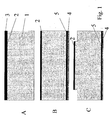
- Fig. 1 illustrates an embodiment of the present invention whereby a germanium solar cell is produced, passivated by the method according to the present invention.
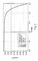
- Fig. 2 and 3 illustrate the performance of a solar cell according to a preferred embodiment of the present invention.
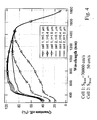
- Fig. 3 illustrates the internal quantum efficiency, the external quantum efficiency and the reflectance of a solar cell created by a preferred embodiment of the present invention, as a function of the wavelength of the incoming light.
- Fig. 4 shows simulation results were the emitter thickness and surface recombination velocities have been varied
- Fig. 5 the carrier lifetime is plotted in function of the duration of the exposure time of the substrate to the H 2 plasma during the preliminary cleaning step.
- the present invention discloses a novel method for passivating and contacting a germanium surface.
- the germanium surface is a surface of a germanium solar cell.
- the method according to the present invention comprises the steps of;
- the method of the invention can be used for the production of a germanium solar cell.
- the method comprises the steps (Fig. 1):
- a preferred embodiment of the method according to the present invention for the production of a germanium solar cell comprises the steps (Fig. 1):
- Fig. 2 and 3 illustrate the performance of a solar cell according to a preferred embodiment of the present invention.
- the short circuit current (J sc ) is equal to 45.8 mA/cm 2
- the open circuit voltage Voc is equal to 245 mV
- the fill factor (FF) was found to be 59.6%.
- An AM1.5 efficiency of 6.7 % was measured.
- Fig. 3 illustrates the internal quantum efficiency, the external quantum efficiency and the reflectance of a solar cell created by a preferred embodiment of the present invention, in function of the wavelength of the incoming light.
- Fig. 4 shows simulation results were the emitter thickness and surface recombination velocities have been varied, cell 1 has a simulated front surface recombination velocity (S front ) of 70000 cm/s and cell 2 has S front equal to 50 cm/s. With decreasing emitter depth and decreasing recombination velocity at the front surface the response of the cell improves.
- the quality of the passivation layer is strongly affected by the cleaning treatment preceding the deposition.
- a H 2 plasma can be used to prepare the surface.
- the measured effective minority carrier lifetime is plotted in function of the duration of the exposure time of the substrate to the H 2 plasma during the preliminary cleaning step. The amount of exposure plays a significant role in the optimisation of the solar cell efficiency.
Landscapes
- Photovoltaic Devices (AREA)
Abstract
- providing said germanium substrate with a first surface;
- producing a passivation layer of amorphous silicon material on said first surface;
- producing a contact layer of metal on said passivation layer;
- applying a diffusion step, such that said germanium surface is contacted by said contact layer, through said passivation layer.
Description
It is a further aim of the invention to provide a novel highly efficient germanium solar cell and a method for producing such a cell.
An improvement of the quality of the passivation is achieved by optimizing the layer thickness. A too thin layer results in lower quality passivation properties, while a too thick layer absorbs a bigger part of the solar spectrum. For application in a mechanically stacked solar cell, or in a TPV cell the restrictions concerning the thickness are less stringent since in these applications the part of the spectrum that is used by the germanium cell will not be absorbed in the amorphous silicon layer.
The effect of the diffusion is that metal particles of the contact layer penetrate into the amorphous silicon passivation layer to form a conductive path between the contact and the Ge-substrate. The resulting contacting resistivity is preferably lower than 5.10-4Ωcm2, more preferably lower than 10-4Ωcm2, most preferably lower than 10-5Ωcm2. The diffusion temperature is preferably between 150 and 300°C, for
Claims (21)
- Method for the passivation and contacting of a surface of a germanium substrate, comprising the steps of;providing said germanium substrate with a first surface;producing a passivation layer of amorphous silicon material on said first surface;producing a contact layer of metal on said passivation layer;applying a diffusion step, such that said germanium surface is contacted by said contact layer, through said passivation layer.
- The method according to claim 1, wherein said diffusion step is performed at a temperature lower than 300°C.
- The method according to claim 2, wherein said diffusion step is performed at a temperature between 160 and 220 °C.
- The method according to any one of claims 1 to 3, wherein said diffusion step uses a diffusion time between 5 and 60 minutes.
- The method according to any one of claims 1 to 4, whereby the contact resistivity after said diffusion step is smaller than 5.10-4Ωcm2.
- The method according to claim 5, whereby said contact resistivity is smaller than 10-4Ωcm2 .
- The method according to claim 6, whereby said contact resistivity is smaller than 10-5Ωcm2.
- The method according to any one of claims 1 to 7, further comprising a step of cleaning said germanium surface before the step of producing said passivation layer, said cleaning step comprising a step of applying a H2 containing plasma to said germanium surface.
- The method according to any one of claims 1 to 8, whereby said step of producing said passivation layer is performed by a Plasma Enhanced Chemical Vapour Deposition.
- The method according to claim 9, whereby said PECVD step is performed at temperatures between 150 to 300°C.
- The method according to any one of claims 1 to 10, whereby said passivation layer has a thickness smaller than 100nm.
- The method according to claim 11, whereby said passivation layer has a thickness smaller than 40nm.
- The method according to claim 11, whereby said passivation layer has a thickness comprised between 10nm and 50nm.
- The method according to any one of claims 1 to 13, wherein said germanium surface is a surface of a germanium solar cell, a thermophotovoltaic cell or a photodetector.
- The method according to any one of claims 1 to 14, wherein said contact layer comprises Ag or Au.
- The method according to any one of claims 1 to 15, wherein said contact layer is patterned to form a contact grid.
- The method according to any one of claims 1 to 16 for the production of a germanium photovoltaic device, further comprising the following steps, said steps being performed before the step of producing a passivation layer of amorphous silicon material on said first surface :producing an emitter area in said germanium substrate,producing a back contact on a second surface of said germanium substrate and realisation of a back surface field,Defining photovoltaic cell areas by etching MESA structures.
- The method according to claim 17, further comprising the step of producing an antireflective coating on the exposed parts of said passivation layer and said contact layer, said step being performed after the step of applying a diffusion step.
- A passivated germanium substrate, comprisinga germanium substrate comprising a first surface;a passivation layer of PECVD deposited amorphous silicon material on said first surface;a metal contacting layer on said passivation layer, contacting said substrate through said passivation layer, by particles of said metal having penetrated into said passivation layer and thereby having formed a conductive path between said contacting layer and said germanium substrate.
- The device according to claim 19, whereby said passivation layer has a thickness comprised between 10 and 50 nm.
- A photovoltaic device comprising a passivated germanium substrate according to claim 19 or 20.
Applications Claiming Priority (2)
| Application Number | Priority Date | Filing Date | Title |
|---|---|---|---|
| US46875203P | 2003-05-07 | 2003-05-07 | |
| US468752P | 2003-05-07 |
Publications (3)
| Publication Number | Publication Date |
|---|---|
| EP1475844A2 true EP1475844A2 (en) | 2004-11-10 |
| EP1475844A3 EP1475844A3 (en) | 2014-12-10 |
| EP1475844B1 EP1475844B1 (en) | 2018-03-07 |
Family
ID=32991000
Family Applications (1)
| Application Number | Title | Priority Date | Filing Date |
|---|---|---|---|
| EP04447115.9A Expired - Lifetime EP1475844B1 (en) | 2003-05-07 | 2004-05-07 | Germanium solar cell and method for the production thereof |
Country Status (3)
| Country | Link |
|---|---|
| US (1) | US7964789B2 (en) |
| EP (1) | EP1475844B1 (en) |
| ES (1) | ES2670168T3 (en) |
Cited By (7)
| Publication number | Priority date | Publication date | Assignee | Title |
|---|---|---|---|---|
| WO2006110048A1 (en) * | 2005-04-14 | 2006-10-19 | Renewable Energy Corporation Asa | Surface passivation of silicon based wafers |
| RU2377698C1 (en) * | 2008-10-28 | 2009-12-27 | Учреждение Российской академии наук Физико-технический институт им. А.Ф. Иоффе РАН | Method of making photoelectric element based on germanium |
| RU2377697C1 (en) * | 2008-11-06 | 2009-12-27 | Учреждение Российской академии наук Физико-технический институт им. А.Ф. Иоффе РАН | Method of making photoelectric converter based on germanium |
| US20120329197A1 (en) * | 2011-04-06 | 2012-12-27 | International Business Machines Corporation | Method of bonding and formation of back surface field (bsf) for multi-junction iii-v solar cells |
| EP1772907A3 (en) * | 2005-10-07 | 2014-12-10 | Imec | Germanium solar cell and method for the production thereof |
| US9099596B2 (en) | 2011-07-29 | 2015-08-04 | International Business Machines Corporation | Heterojunction photovoltaic device and fabrication method |
| CN105122462B (en) * | 2012-12-21 | 2018-08-17 | 太阳能公司 | The seed layer that adhesion strength for solar cell conductive contact enhances |
Families Citing this family (41)
| Publication number | Priority date | Publication date | Assignee | Title |
|---|---|---|---|---|
| DE102004005050A1 (en) * | 2004-01-30 | 2005-08-25 | Detlef Schulz | Method for energy conversion of solar radiation into electricity and heat with color-selective interference filter mirrors and a device of a concentrator solar collector with color-selective mirrors for the application of the method |
| US7906722B2 (en) * | 2005-04-19 | 2011-03-15 | Palo Alto Research Center Incorporated | Concentrating solar collector with solid optical element |
| US20070169806A1 (en) * | 2006-01-20 | 2007-07-26 | Palo Alto Research Center Incorporated | Solar cell production using non-contact patterning and direct-write metallization |
| US20070107773A1 (en) * | 2005-11-17 | 2007-05-17 | Palo Alto Research Center Incorporated | Bifacial cell with extruded gridline metallization |
| US7799371B2 (en) * | 2005-11-17 | 2010-09-21 | Palo Alto Research Center Incorporated | Extruding/dispensing multiple materials to form high-aspect ratio extruded structures |
| US7765949B2 (en) | 2005-11-17 | 2010-08-03 | Palo Alto Research Center Incorporated | Extrusion/dispensing systems and methods |
| US7851693B2 (en) * | 2006-05-05 | 2010-12-14 | Palo Alto Research Center Incorporated | Passively cooled solar concentrating photovoltaic device |
| US7638708B2 (en) * | 2006-05-05 | 2009-12-29 | Palo Alto Research Center Incorporated | Laminated solar concentrating photovoltaic device |
| US7780812B2 (en) * | 2006-11-01 | 2010-08-24 | Palo Alto Research Center Incorporated | Extrusion head with planarized edge surface |
| US7922471B2 (en) * | 2006-11-01 | 2011-04-12 | Palo Alto Research Center Incorporated | Extruded structure with equilibrium shape |
| US8226391B2 (en) * | 2006-11-01 | 2012-07-24 | Solarworld Innovations Gmbh | Micro-extrusion printhead nozzle with tapered cross-section |
| US8322025B2 (en) | 2006-11-01 | 2012-12-04 | Solarworld Innovations Gmbh | Apparatus for forming a plurality of high-aspect ratio gridline structures |
| US20080116182A1 (en) * | 2006-11-21 | 2008-05-22 | Palo Alto Research Center Incorporated | Multiple Station Scan Displacement Invariant Laser Ablation Apparatus |
| US20080116183A1 (en) * | 2006-11-21 | 2008-05-22 | Palo Alto Research Center Incorporated | Light Scanning Mechanism For Scan Displacement Invariant Laser Ablation Apparatus |
| US7928015B2 (en) * | 2006-12-12 | 2011-04-19 | Palo Alto Research Center Incorporated | Solar cell fabrication using extruded dopant-bearing materials |
| US7638438B2 (en) * | 2006-12-12 | 2009-12-29 | Palo Alto Research Center Incorporated | Solar cell fabrication using extrusion mask |
| US20090025789A1 (en) * | 2007-02-02 | 2009-01-29 | Hing Wah Chan | Alignment of optical element and solar cell |
| US7954449B2 (en) * | 2007-05-08 | 2011-06-07 | Palo Alto Research Center Incorporated | Wiring-free, plumbing-free, cooled, vacuum chuck |
| US8071872B2 (en) | 2007-06-15 | 2011-12-06 | Translucent Inc. | Thin film semi-conductor-on-glass solar cell devices |
| US9287438B1 (en) * | 2008-07-16 | 2016-03-15 | Solaero Technologies Corp. | Method for forming ohmic N-contacts at low temperature in inverted metamorphic multijunction solar cells with contaminant isolation |
| US7999175B2 (en) * | 2008-09-09 | 2011-08-16 | Palo Alto Research Center Incorporated | Interdigitated back contact silicon solar cells with laser ablated grooves |
| US8117983B2 (en) * | 2008-11-07 | 2012-02-21 | Solarworld Innovations Gmbh | Directional extruded bead control |
| US20100221435A1 (en) * | 2008-11-07 | 2010-09-02 | Palo Alto Research Center Incorporated | Micro-Extrusion System With Airjet Assisted Bead Deflection |
| US20100117254A1 (en) * | 2008-11-07 | 2010-05-13 | Palo Alto Research Center Incorporated | Micro-Extrusion System With Airjet Assisted Bead Deflection |
| US20100118081A1 (en) * | 2008-11-07 | 2010-05-13 | Palo Alto Research Center Incorporated | Dead Volume Removal From An Extrusion Printhead |
| US9150966B2 (en) * | 2008-11-14 | 2015-10-06 | Palo Alto Research Center Incorporated | Solar cell metallization using inline electroless plating |
| US8080729B2 (en) * | 2008-11-24 | 2011-12-20 | Palo Alto Research Center Incorporated | Melt planarization of solar cell bus bars |
| US20100130014A1 (en) * | 2008-11-26 | 2010-05-27 | Palo Alto Research Center Incorporated | Texturing multicrystalline silicon |
| US20100139754A1 (en) * | 2008-12-09 | 2010-06-10 | Palo Alto Research Center Incorporated | Solar Cell With Co-Planar Backside Metallization |
| US8960120B2 (en) * | 2008-12-09 | 2015-02-24 | Palo Alto Research Center Incorporated | Micro-extrusion printhead with nozzle valves |
| US20100139756A1 (en) * | 2008-12-10 | 2010-06-10 | Palo Alto Research Center Incorporated | Simultaneously Writing Bus Bars And Gridlines For Solar Cell |
| US20100206379A1 (en) * | 2009-02-18 | 2010-08-19 | Palo Alto Research Center Incorporated | Rotational Trough Reflector Array With Solid Optical Element For Solar-Electricity Generation |
| US20100206302A1 (en) * | 2009-02-18 | 2010-08-19 | Palo Alto Research Center Incorporated | Rotational Trough Reflector Array For Solar-Electricity Generation |
| US20100206357A1 (en) * | 2009-02-18 | 2010-08-19 | Palo Alto Research Center Incorporated | Two-Part Solar Energy Collection System With Replaceable Solar Collector Component |
| US20110083728A1 (en) * | 2009-10-14 | 2011-04-14 | Palo Alto Research Center Incorporated | Disordered Nanowire Solar Cell |
| US20110100419A1 (en) * | 2009-11-03 | 2011-05-05 | Palo Alto Research Center Incorporated | Linear Concentrating Solar Collector With Decentered Trough-Type Relectors |
| US20110216401A1 (en) * | 2010-03-03 | 2011-09-08 | Palo Alto Research Center Incorporated | Scanning System With Orbiting Objective |
| EP2461352B1 (en) | 2010-12-06 | 2013-07-10 | Imec | Method of manufacturing low resistivity contacts on n-type germanium |
| US8962424B2 (en) | 2011-03-03 | 2015-02-24 | Palo Alto Research Center Incorporated | N-type silicon solar cell with contact/protection structures |
| FI127415B (en) | 2015-04-16 | 2018-05-31 | Turun Yliopisto | Preparation of foreign oxide on semiconductors |
| CN111509055B (en) * | 2020-03-20 | 2024-03-05 | 中国科学院宁波材料技术与工程研究所 | Interface laminated film, preparation method thereof and application in passivated contact battery |
Family Cites Families (24)
| Publication number | Priority date | Publication date | Assignee | Title |
|---|---|---|---|---|
| GB1355890A (en) * | 1972-04-29 | 1974-06-05 | Ferranti Ltd | Contacts for solar cells |
| US4742384A (en) * | 1978-02-01 | 1988-05-03 | Rca Corporation | Structure for passivating a PN junction |
| US4473597A (en) | 1978-02-01 | 1984-09-25 | Rca Corporation | Method and structure for passivating a PN junction |
| US4319395A (en) * | 1979-06-28 | 1982-03-16 | Motorola, Inc. | Method of making self-aligned device |
| JPS56155526A (en) | 1980-05-06 | 1981-12-01 | Shunpei Yamazaki | Method of forming film |
| EP0078541B1 (en) * | 1981-11-04 | 1991-01-16 | Kanegafuchi Kagaku Kogyo Kabushiki Kaisha | Flexible photovoltaic device |
| JPS58197717A (en) | 1982-05-13 | 1983-11-17 | Toshiba Corp | Preparation of semiconductor device |
| US4589006A (en) * | 1982-08-23 | 1986-05-13 | The United States Of America As Represented By The United States Department Of Energy | Germanium detector passivated with hydrogenated amorphous germanium |
| US4602120A (en) * | 1983-11-25 | 1986-07-22 | Atlantic Richfield Company | Solar cell manufacture |
| DE3854040T2 (en) * | 1987-11-20 | 1995-10-26 | Canon Kk | Photovoltaic PIN component, tandem and triple cells. |
| JPH03502627A (en) | 1988-06-10 | 1991-06-13 | エイエスイー・アメリカス・インコーポレーテッド | Improved method of making contacts for solar cells |
| DE69103251T2 (en) * | 1990-11-30 | 1994-11-24 | Agency Ind Science Techn | Process for forming an amorphous silicon thin film using plasma CVD. |
| JPH0548127A (en) * | 1991-08-19 | 1993-02-26 | Showa Shell Sekiyu Kk | Amorphous silicon solar cell and manufacturing method thereof |
| US5437736A (en) | 1994-02-15 | 1995-08-01 | Cole; Eric D. | Semiconductor fiber solar cells and modules |
| JP3459947B2 (en) * | 1996-06-18 | 2003-10-27 | シャープ株式会社 | Solar cell manufacturing method |
| US7176111B2 (en) * | 1997-03-28 | 2007-02-13 | Interuniversitair Microelektronica Centrum (Imec) | Method for depositing polycrystalline SiGe suitable for micromachining and devices obtained thereof |
| AUPO638997A0 (en) * | 1997-04-23 | 1997-05-22 | Unisearch Limited | Metal contact scheme using selective silicon growth |
| US6339013B1 (en) * | 1997-05-13 | 2002-01-15 | The Board Of Trustees Of The University Of Arkansas | Method of doping silicon, metal doped silicon, method of making solar cells, and solar cells |
| US6103970A (en) * | 1998-08-20 | 2000-08-15 | Tecstar Power Systems, Inc. | Solar cell having a front-mounted bypass diode |
| US6632730B1 (en) * | 1999-11-23 | 2003-10-14 | Ebara Solar, Inc. | Method for self-doping contacts to a semiconductor |
| JP3586197B2 (en) | 2000-03-23 | 2004-11-10 | シャープ株式会社 | Plasma film forming equipment for thin film formation |
| DE60139610D1 (en) | 2000-04-05 | 2009-10-01 | Imec | METHOD FOR SEPARATING A POLYCRYSTALLINE SUITABLE FOR MICRO-PROCESSING |
| DE10046170A1 (en) * | 2000-09-19 | 2002-04-04 | Fraunhofer Ges Forschung | Method for producing a semiconductor-metal contact through a dielectric layer |
| US6645831B1 (en) | 2002-05-07 | 2003-11-11 | Intel Corporation | Thermally stable crystalline defect-free germanium bonded to silicon and silicon dioxide |
-
2004
- 2004-05-06 US US10/841,803 patent/US7964789B2/en active Active
- 2004-05-07 EP EP04447115.9A patent/EP1475844B1/en not_active Expired - Lifetime
- 2004-05-07 ES ES04447115.9T patent/ES2670168T3/en not_active Expired - Lifetime
Cited By (12)
| Publication number | Priority date | Publication date | Assignee | Title |
|---|---|---|---|---|
| WO2006110048A1 (en) * | 2005-04-14 | 2006-10-19 | Renewable Energy Corporation Asa | Surface passivation of silicon based wafers |
| US8916768B2 (en) | 2005-04-14 | 2014-12-23 | Rec Solar Pte. Ltd. | Surface passivation of silicon based wafers |
| EP1772907A3 (en) * | 2005-10-07 | 2014-12-10 | Imec | Germanium solar cell and method for the production thereof |
| RU2377698C1 (en) * | 2008-10-28 | 2009-12-27 | Учреждение Российской академии наук Физико-технический институт им. А.Ф. Иоффе РАН | Method of making photoelectric element based on germanium |
| RU2377697C1 (en) * | 2008-11-06 | 2009-12-27 | Учреждение Российской академии наук Физико-технический институт им. А.Ф. Иоффе РАН | Method of making photoelectric converter based on germanium |
| US20120329197A1 (en) * | 2011-04-06 | 2012-12-27 | International Business Machines Corporation | Method of bonding and formation of back surface field (bsf) for multi-junction iii-v solar cells |
| US9099596B2 (en) | 2011-07-29 | 2015-08-04 | International Business Machines Corporation | Heterojunction photovoltaic device and fabrication method |
| US10304984B2 (en) | 2011-07-29 | 2019-05-28 | International Business Machines Corporation | Heterojunction photovoltaic device and fabrication method |
| US10304985B2 (en) | 2011-07-29 | 2019-05-28 | International Business Machines Corporation | Heterojunction photovoltaic device and fabrication method |
| US10672929B2 (en) | 2011-07-29 | 2020-06-02 | International Business Machines Corporation | Heterojunction photovoltaic device and fabrication method |
| US11094842B2 (en) | 2011-07-29 | 2021-08-17 | International Business Machines Corporation | Heterojunction photovoltaic device and fabrication method |
| CN105122462B (en) * | 2012-12-21 | 2018-08-17 | 太阳能公司 | The seed layer that adhesion strength for solar cell conductive contact enhances |
Also Published As
| Publication number | Publication date |
|---|---|
| US7964789B2 (en) | 2011-06-21 |
| EP1475844A3 (en) | 2014-12-10 |
| US20050000566A1 (en) | 2005-01-06 |
| ES2670168T3 (en) | 2018-05-29 |
| EP1475844B1 (en) | 2018-03-07 |
Similar Documents
| Publication | Publication Date | Title |
|---|---|---|
| EP1475844B1 (en) | Germanium solar cell and method for the production thereof | |
| JP7168809B1 (en) | SOLAR CELL AND MANUFACTURING METHOD THEREOF, PHOTOVOLTAIC MODULE | |
| US9608131B2 (en) | Solar cell having doped semiconductor heterojunction contacts | |
| US8664525B2 (en) | Germanium solar cell and method for the production thereof | |
| US8349644B2 (en) | Mono-silicon solar cells | |
| CN100524840C (en) | Hetero-contact solar cell with reversed geometry in layer structure | |
| US4253881A (en) | Solar cells composed of semiconductive materials | |
| EP1231648B1 (en) | Solar cell and manufacturing method thereof | |
| EP2469605A2 (en) | Substrate for photoelectric conversion device, photoelectric conversion device, and stacked photoelectric conversion device | |
| US20110162699A1 (en) | Solar cell with funnel-like groove structure | |
| US20100243042A1 (en) | High-efficiency photovoltaic cells | |
| US9768329B1 (en) | Multi-junction optoelectronic device | |
| JP7336569B1 (en) | SOLAR CELL AND MANUFACTURING METHOD THEREOF, PHOTOVOLTAIC MODULE | |
| CN108352421A (en) | Solar cell with the multiple absorbers interconnected by carrier selectivity contact | |
| CN110943143A (en) | Method for manufacturing a photovoltaic solar cell with heterojunction and emitter diffusion regions | |
| US11271128B2 (en) | Multi-junction optoelectronic device | |
| KR101370225B1 (en) | Method of preparing solar cell and solar cell prepared by the same | |
| US7960645B2 (en) | Germanium solar cell and method for the production thereof | |
| Muller et al. | Self-aligning, industrially feasible back contacted silicon solar cells with efficiencies> 18% | |
| Duan et al. | Ultrathin crystalline silicon heterojunction solar cell integrated on silicon-on-insulator substrate | |
| van der Heide et al. | email: Johan. vanderheide (imec. be--. |
Legal Events
| Date | Code | Title | Description |
|---|---|---|---|
| PUAI | Public reference made under article 153(3) epc to a published international application that has entered the european phase |
Free format text: ORIGINAL CODE: 0009012 |
|
| AK | Designated contracting states |
Kind code of ref document: A2 Designated state(s): AT BE BG CH CY CZ DE DK EE ES FI FR GB GR HU IE IT LI LU MC NL PL PT RO SE SI SK TR |
|
| AX | Request for extension of the european patent |
Extension state: AL LT LV MK |
|
| RAP1 | Party data changed (applicant data changed or rights of an application transferred) |
Owner name: INTERUNIVERSITAIR MICROELEKTRONICA CENTRUM VZW Owner name: UMICORE N.V. |
|
| RAP1 | Party data changed (applicant data changed or rights of an application transferred) |
Owner name: UMICORE N.V. Owner name: IMEC |
|
| PUAL | Search report despatched |
Free format text: ORIGINAL CODE: 0009013 |
|
| AK | Designated contracting states |
Kind code of ref document: A3 Designated state(s): AT BE BG CH CY CZ DE DK EE ES FI FR GB GR HU IE IT LI LU MC NL PL PT RO SE SI SK TR |
|
| AX | Request for extension of the european patent |
Extension state: AL LT LV MK |
|
| RIC1 | Information provided on ipc code assigned before grant |
Ipc: H01L 31/0224 20060101ALI20141104BHEP Ipc: H01L 31/18 20060101AFI20141104BHEP Ipc: H01L 31/028 20060101ALI20141104BHEP Ipc: H01L 31/0216 20140101ALI20141104BHEP |
|
| 17P | Request for examination filed |
Effective date: 20150610 |
|
| RAX | Requested extension states of the european patent have changed |
Extension state: MK Payment date: 20150610 Extension state: LT Payment date: 20150610 Extension state: AL Payment date: 20150610 Extension state: LV Payment date: 20150610 |
|
| RBV | Designated contracting states (corrected) |
Designated state(s): AT BE BG CH CY CZ DE DK EE ES FI FR GB GR HU IE IT LI LU MC NL PL PT RO SE SI SK TR |
|
| 17Q | First examination report despatched |
Effective date: 20150625 |
|
| AKX | Designation fees paid |
Designated state(s): AT BE BG CH CY CZ DE DK EE ES FI FR GB GR HU IE IT LI LU MC NL PL PT RO SE SI SK TR |
|
| AXX | Extension fees paid |
Extension state: LV Payment date: 20150610 Extension state: MK Payment date: 20150610 Extension state: AL Payment date: 20150610 Extension state: LT Payment date: 20150610 |
|
| GRAP | Despatch of communication of intention to grant a patent |
Free format text: ORIGINAL CODE: EPIDOSNIGR1 |
|
| INTG | Intention to grant announced |
Effective date: 20170929 |
|
| RIN1 | Information on inventor provided before grant (corrected) |
Inventor name: FLAMAND, GIOVANNI Inventor name: POORTMANS, JEF Inventor name: POSTHUMA, NIELS |
|
| RAP1 | Party data changed (applicant data changed or rights of an application transferred) |
Owner name: UMICORE N.V. Owner name: IMEC VZW |
|
| GRAS | Grant fee paid |
Free format text: ORIGINAL CODE: EPIDOSNIGR3 |
|
| GRAA | (expected) grant |
Free format text: ORIGINAL CODE: 0009210 |
|
| AK | Designated contracting states |
Kind code of ref document: B1 Designated state(s): AT BE BG CH CY CZ DE DK EE ES FI FR GB GR HU IE IT LI LU MC NL PL PT RO SE SI SK TR |
|
| AX | Request for extension of the european patent |
Extension state: AL LT LV MK |
|
| REG | Reference to a national code |
Ref country code: GB Ref legal event code: FG4D |
|
| REG | Reference to a national code |
Ref country code: CH Ref legal event code: EP Ref country code: AT Ref legal event code: REF Ref document number: 977421 Country of ref document: AT Kind code of ref document: T Effective date: 20180315 |
|
| REG | Reference to a national code |
Ref country code: DE Ref legal event code: R096 Ref document number: 602004052427 Country of ref document: DE |
|
| REG | Reference to a national code |
Ref country code: IE Ref legal event code: FG4D |
|
| REG | Reference to a national code |
Ref country code: FR Ref legal event code: PLFP Year of fee payment: 15 |
|
| REG | Reference to a national code |
Ref country code: ES Ref legal event code: FG2A Ref document number: 2670168 Country of ref document: ES Kind code of ref document: T3 Effective date: 20180529 |
|
| REG | Reference to a national code |
Ref country code: NL Ref legal event code: FP |
|
| REG | Reference to a national code |
Ref country code: LT Ref legal event code: MG9D |
|
| PG25 | Lapsed in a contracting state [announced via postgrant information from national office to epo] |
Ref country code: CY Free format text: LAPSE BECAUSE OF FAILURE TO SUBMIT A TRANSLATION OF THE DESCRIPTION OR TO PAY THE FEE WITHIN THE PRESCRIBED TIME-LIMIT Effective date: 20180307 Ref country code: FI Free format text: LAPSE BECAUSE OF FAILURE TO SUBMIT A TRANSLATION OF THE DESCRIPTION OR TO PAY THE FEE WITHIN THE PRESCRIBED TIME-LIMIT Effective date: 20180307 |
|
| PG25 | Lapsed in a contracting state [announced via postgrant information from national office to epo] |
Ref country code: GR Free format text: LAPSE BECAUSE OF FAILURE TO SUBMIT A TRANSLATION OF THE DESCRIPTION OR TO PAY THE FEE WITHIN THE PRESCRIBED TIME-LIMIT Effective date: 20180608 Ref country code: SE Free format text: LAPSE BECAUSE OF FAILURE TO SUBMIT A TRANSLATION OF THE DESCRIPTION OR TO PAY THE FEE WITHIN THE PRESCRIBED TIME-LIMIT Effective date: 20180307 Ref country code: BG Free format text: LAPSE BECAUSE OF FAILURE TO SUBMIT A TRANSLATION OF THE DESCRIPTION OR TO PAY THE FEE WITHIN THE PRESCRIBED TIME-LIMIT Effective date: 20180607 |
|
| PG25 | Lapsed in a contracting state [announced via postgrant information from national office to epo] |
Ref country code: EE Free format text: LAPSE BECAUSE OF FAILURE TO SUBMIT A TRANSLATION OF THE DESCRIPTION OR TO PAY THE FEE WITHIN THE PRESCRIBED TIME-LIMIT Effective date: 20180307 Ref country code: PL Free format text: LAPSE BECAUSE OF FAILURE TO SUBMIT A TRANSLATION OF THE DESCRIPTION OR TO PAY THE FEE WITHIN THE PRESCRIBED TIME-LIMIT Effective date: 20180307 Ref country code: RO Free format text: LAPSE BECAUSE OF FAILURE TO SUBMIT A TRANSLATION OF THE DESCRIPTION OR TO PAY THE FEE WITHIN THE PRESCRIBED TIME-LIMIT Effective date: 20180307 |
|
| PG25 | Lapsed in a contracting state [announced via postgrant information from national office to epo] |
Ref country code: CZ Free format text: LAPSE BECAUSE OF FAILURE TO SUBMIT A TRANSLATION OF THE DESCRIPTION OR TO PAY THE FEE WITHIN THE PRESCRIBED TIME-LIMIT Effective date: 20180307 Ref country code: SK Free format text: LAPSE BECAUSE OF FAILURE TO SUBMIT A TRANSLATION OF THE DESCRIPTION OR TO PAY THE FEE WITHIN THE PRESCRIBED TIME-LIMIT Effective date: 20180307 |
|
| REG | Reference to a national code |
Ref country code: DE Ref legal event code: R097 Ref document number: 602004052427 Country of ref document: DE |
|
| PG25 | Lapsed in a contracting state [announced via postgrant information from national office to epo] |
Ref country code: PT Free format text: LAPSE BECAUSE OF FAILURE TO SUBMIT A TRANSLATION OF THE DESCRIPTION OR TO PAY THE FEE WITHIN THE PRESCRIBED TIME-LIMIT Effective date: 20180709 |
|
| PLBE | No opposition filed within time limit |
Free format text: ORIGINAL CODE: 0009261 |
|
| STAA | Information on the status of an ep patent application or granted ep patent |
Free format text: STATUS: NO OPPOSITION FILED WITHIN TIME LIMIT |
|
| PG25 | Lapsed in a contracting state [announced via postgrant information from national office to epo] |
Ref country code: DK Free format text: LAPSE BECAUSE OF FAILURE TO SUBMIT A TRANSLATION OF THE DESCRIPTION OR TO PAY THE FEE WITHIN THE PRESCRIBED TIME-LIMIT Effective date: 20180307 Ref country code: MC Free format text: LAPSE BECAUSE OF FAILURE TO SUBMIT A TRANSLATION OF THE DESCRIPTION OR TO PAY THE FEE WITHIN THE PRESCRIBED TIME-LIMIT Effective date: 20180307 |
|
| 26N | No opposition filed |
Effective date: 20181210 |
|
| REG | Reference to a national code |
Ref country code: IE Ref legal event code: MM4A |
|
| PG25 | Lapsed in a contracting state [announced via postgrant information from national office to epo] |
Ref country code: SI Free format text: LAPSE BECAUSE OF FAILURE TO SUBMIT A TRANSLATION OF THE DESCRIPTION OR TO PAY THE FEE WITHIN THE PRESCRIBED TIME-LIMIT Effective date: 20180307 |
|
| PG25 | Lapsed in a contracting state [announced via postgrant information from national office to epo] |
Ref country code: LU Free format text: LAPSE BECAUSE OF NON-PAYMENT OF DUE FEES Effective date: 20180507 |
|
| PG25 | Lapsed in a contracting state [announced via postgrant information from national office to epo] |
Ref country code: IE Free format text: LAPSE BECAUSE OF NON-PAYMENT OF DUE FEES Effective date: 20180507 |
|
| PG25 | Lapsed in a contracting state [announced via postgrant information from national office to epo] |
Ref country code: TR Free format text: LAPSE BECAUSE OF FAILURE TO SUBMIT A TRANSLATION OF THE DESCRIPTION OR TO PAY THE FEE WITHIN THE PRESCRIBED TIME-LIMIT Effective date: 20180307 |
|
| PG25 | Lapsed in a contracting state [announced via postgrant information from national office to epo] |
Ref country code: HU Free format text: LAPSE BECAUSE OF FAILURE TO SUBMIT A TRANSLATION OF THE DESCRIPTION OR TO PAY THE FEE WITHIN THE PRESCRIBED TIME-LIMIT; INVALID AB INITIO Effective date: 20040507 |
|
| REG | Reference to a national code |
Ref country code: AT Ref legal event code: UEP Ref document number: 977421 Country of ref document: AT Kind code of ref document: T Effective date: 20180307 |
|
| PGFP | Annual fee paid to national office [announced via postgrant information from national office to epo] |
Ref country code: FR Payment date: 20230309 Year of fee payment: 20 |
|
| PGFP | Annual fee paid to national office [announced via postgrant information from national office to epo] |
Ref country code: GB Payment date: 20230316 Year of fee payment: 20 |
|
| PGFP | Annual fee paid to national office [announced via postgrant information from national office to epo] |
Ref country code: NL Payment date: 20230314 Year of fee payment: 20 |
|
| P01 | Opt-out of the competence of the unified patent court (upc) registered |
Effective date: 20230602 |
|
| PGFP | Annual fee paid to national office [announced via postgrant information from national office to epo] |
Ref country code: IT Payment date: 20230412 Year of fee payment: 20 Ref country code: ES Payment date: 20230601 Year of fee payment: 20 Ref country code: DE Payment date: 20230314 Year of fee payment: 20 Ref country code: CH Payment date: 20230602 Year of fee payment: 20 |
|
| PGFP | Annual fee paid to national office [announced via postgrant information from national office to epo] |
Ref country code: AT Payment date: 20230425 Year of fee payment: 20 |
|
| PGFP | Annual fee paid to national office [announced via postgrant information from national office to epo] |
Ref country code: BE Payment date: 20230418 Year of fee payment: 20 |
|
| REG | Reference to a national code |
Ref country code: DE Ref legal event code: R071 Ref document number: 602004052427 Country of ref document: DE |
|
| REG | Reference to a national code |
Ref country code: NL Ref legal event code: MK Effective date: 20240506 |
|
| REG | Reference to a national code |
Ref country code: CH Ref legal event code: PL |
|
| REG | Reference to a national code |
Ref country code: ES Ref legal event code: FD2A Effective date: 20240524 |
|
| REG | Reference to a national code |
Ref country code: BE Ref legal event code: MK Effective date: 20240507 |
|
| REG | Reference to a national code |
Ref country code: GB Ref legal event code: PE20 Expiry date: 20240506 |
|
| REG | Reference to a national code |
Ref country code: AT Ref legal event code: MK07 Ref document number: 977421 Country of ref document: AT Kind code of ref document: T Effective date: 20240507 |
|
| PG25 | Lapsed in a contracting state [announced via postgrant information from national office to epo] |
Ref country code: GB Free format text: LAPSE BECAUSE OF EXPIRATION OF PROTECTION Effective date: 20240506 |
|
| PG25 | Lapsed in a contracting state [announced via postgrant information from national office to epo] |
Ref country code: ES Free format text: LAPSE BECAUSE OF EXPIRATION OF PROTECTION Effective date: 20240508 |
|
| PG25 | Lapsed in a contracting state [announced via postgrant information from national office to epo] |
Ref country code: GB Free format text: LAPSE BECAUSE OF EXPIRATION OF PROTECTION Effective date: 20240506 Ref country code: ES Free format text: LAPSE BECAUSE OF EXPIRATION OF PROTECTION Effective date: 20240508 |