EP1498468A1 - Liquid-crystal display - Google Patents
Liquid-crystal display Download PDFInfo
- Publication number
- EP1498468A1 EP1498468A1 EP03746491A EP03746491A EP1498468A1 EP 1498468 A1 EP1498468 A1 EP 1498468A1 EP 03746491 A EP03746491 A EP 03746491A EP 03746491 A EP03746491 A EP 03746491A EP 1498468 A1 EP1498468 A1 EP 1498468A1
- Authority
- EP
- European Patent Office
- Prior art keywords
- liquid crystal
- crystal display
- display device
- monomer
- substrates
- Prior art date
- Legal status (The legal status is an assumption and is not a legal conclusion. Google has not performed a legal analysis and makes no representation as to the accuracy of the status listed.)
- Granted
Links
Images

Classifications
-
- C—CHEMISTRY; METALLURGY
- C09—DYES; PAINTS; POLISHES; NATURAL RESINS; ADHESIVES; COMPOSITIONS NOT OTHERWISE PROVIDED FOR; APPLICATIONS OF MATERIALS NOT OTHERWISE PROVIDED FOR
- C09K—MATERIALS FOR MISCELLANEOUS APPLICATIONS, NOT PROVIDED FOR ELSEWHERE
- C09K19/00—Liquid crystal materials
- C09K19/04—Liquid crystal materials characterised by the chemical structure of the liquid crystal components, e.g. by a specific unit
- C09K19/06—Non-steroidal liquid crystal compounds
- C09K19/08—Non-steroidal liquid crystal compounds containing at least two non-condensed rings
- C09K19/10—Non-steroidal liquid crystal compounds containing at least two non-condensed rings containing at least two benzene rings
- C09K19/12—Non-steroidal liquid crystal compounds containing at least two non-condensed rings containing at least two benzene rings at least two benzene rings directly linked, e.g. biphenyls
-
- G—PHYSICS
- G02—OPTICS
- G02F—OPTICAL DEVICES OR ARRANGEMENTS FOR THE CONTROL OF LIGHT BY MODIFICATION OF THE OPTICAL PROPERTIES OF THE MEDIA OF THE ELEMENTS INVOLVED THEREIN; NON-LINEAR OPTICS; FREQUENCY-CHANGING OF LIGHT; OPTICAL LOGIC ELEMENTS; OPTICAL ANALOGUE/DIGITAL CONVERTERS
- G02F1/00—Devices or arrangements for the control of the intensity, colour, phase, polarisation or direction of light arriving from an independent light source, e.g. switching, gating or modulating; Non-linear optics
- G02F1/01—Devices or arrangements for the control of the intensity, colour, phase, polarisation or direction of light arriving from an independent light source, e.g. switching, gating or modulating; Non-linear optics for the control of the intensity, phase, polarisation or colour
- G02F1/13—Devices or arrangements for the control of the intensity, colour, phase, polarisation or direction of light arriving from an independent light source, e.g. switching, gating or modulating; Non-linear optics for the control of the intensity, phase, polarisation or colour based on liquid crystals, e.g. single liquid crystal display cells
-
- C—CHEMISTRY; METALLURGY
- C08—ORGANIC MACROMOLECULAR COMPOUNDS; THEIR PREPARATION OR CHEMICAL WORKING-UP; COMPOSITIONS BASED THEREON
- C08F—MACROMOLECULAR COMPOUNDS OBTAINED BY REACTIONS ONLY INVOLVING CARBON-TO-CARBON UNSATURATED BONDS
- C08F2/00—Processes of polymerisation
-
- C—CHEMISTRY; METALLURGY
- C09—DYES; PAINTS; POLISHES; NATURAL RESINS; ADHESIVES; COMPOSITIONS NOT OTHERWISE PROVIDED FOR; APPLICATIONS OF MATERIALS NOT OTHERWISE PROVIDED FOR
- C09K—MATERIALS FOR MISCELLANEOUS APPLICATIONS, NOT PROVIDED FOR ELSEWHERE
- C09K19/00—Liquid crystal materials
- C09K19/04—Liquid crystal materials characterised by the chemical structure of the liquid crystal components, e.g. by a specific unit
- C09K19/06—Non-steroidal liquid crystal compounds
- C09K19/08—Non-steroidal liquid crystal compounds containing at least two non-condensed rings
- C09K19/10—Non-steroidal liquid crystal compounds containing at least two non-condensed rings containing at least two benzene rings
- C09K19/20—Non-steroidal liquid crystal compounds containing at least two non-condensed rings containing at least two benzene rings linked by a chain containing carbon and oxygen atoms as chain links, e.g. esters or ethers
- C09K19/2007—Non-steroidal liquid crystal compounds containing at least two non-condensed rings containing at least two benzene rings linked by a chain containing carbon and oxygen atoms as chain links, e.g. esters or ethers the chain containing -COO- or -OCO- groups
-
- C—CHEMISTRY; METALLURGY
- C09—DYES; PAINTS; POLISHES; NATURAL RESINS; ADHESIVES; COMPOSITIONS NOT OTHERWISE PROVIDED FOR; APPLICATIONS OF MATERIALS NOT OTHERWISE PROVIDED FOR
- C09K—MATERIALS FOR MISCELLANEOUS APPLICATIONS, NOT PROVIDED FOR ELSEWHERE
- C09K19/00—Liquid crystal materials
- C09K19/04—Liquid crystal materials characterised by the chemical structure of the liquid crystal components, e.g. by a specific unit
- C09K19/06—Non-steroidal liquid crystal compounds
- C09K19/32—Non-steroidal liquid crystal compounds containing condensed ring systems, i.e. fused, bridged or spiro ring systems
- C09K19/322—Compounds containing a naphthalene ring or a completely or partially hydrogenated naphthalene ring
-
- C—CHEMISTRY; METALLURGY
- C09—DYES; PAINTS; POLISHES; NATURAL RESINS; ADHESIVES; COMPOSITIONS NOT OTHERWISE PROVIDED FOR; APPLICATIONS OF MATERIALS NOT OTHERWISE PROVIDED FOR
- C09K—MATERIALS FOR MISCELLANEOUS APPLICATIONS, NOT PROVIDED FOR ELSEWHERE
- C09K19/00—Liquid crystal materials
- C09K19/04—Liquid crystal materials characterised by the chemical structure of the liquid crystal components, e.g. by a specific unit
- C09K19/06—Non-steroidal liquid crystal compounds
- C09K19/34—Non-steroidal liquid crystal compounds containing at least one heterocyclic ring
-
- C—CHEMISTRY; METALLURGY
- C09—DYES; PAINTS; POLISHES; NATURAL RESINS; ADHESIVES; COMPOSITIONS NOT OTHERWISE PROVIDED FOR; APPLICATIONS OF MATERIALS NOT OTHERWISE PROVIDED FOR
- C09K—MATERIALS FOR MISCELLANEOUS APPLICATIONS, NOT PROVIDED FOR ELSEWHERE
- C09K19/00—Liquid crystal materials
- C09K19/04—Liquid crystal materials characterised by the chemical structure of the liquid crystal components, e.g. by a specific unit
- C09K19/38—Polymers
-
- G—PHYSICS
- G02—OPTICS
- G02F—OPTICAL DEVICES OR ARRANGEMENTS FOR THE CONTROL OF LIGHT BY MODIFICATION OF THE OPTICAL PROPERTIES OF THE MEDIA OF THE ELEMENTS INVOLVED THEREIN; NON-LINEAR OPTICS; FREQUENCY-CHANGING OF LIGHT; OPTICAL LOGIC ELEMENTS; OPTICAL ANALOGUE/DIGITAL CONVERTERS
- G02F1/00—Devices or arrangements for the control of the intensity, colour, phase, polarisation or direction of light arriving from an independent light source, e.g. switching, gating or modulating; Non-linear optics
- G02F1/01—Devices or arrangements for the control of the intensity, colour, phase, polarisation or direction of light arriving from an independent light source, e.g. switching, gating or modulating; Non-linear optics for the control of the intensity, phase, polarisation or colour
- G02F1/13—Devices or arrangements for the control of the intensity, colour, phase, polarisation or direction of light arriving from an independent light source, e.g. switching, gating or modulating; Non-linear optics for the control of the intensity, phase, polarisation or colour based on liquid crystals, e.g. single liquid crystal display cells
- G02F1/133—Constructional arrangements; Operation of liquid crystal cells; Circuit arrangements
- G02F1/1333—Constructional arrangements; Manufacturing methods
- G02F1/133365—Cells in which the active layer comprises a liquid crystalline polymer
-
- G—PHYSICS
- G02—OPTICS
- G02F—OPTICAL DEVICES OR ARRANGEMENTS FOR THE CONTROL OF LIGHT BY MODIFICATION OF THE OPTICAL PROPERTIES OF THE MEDIA OF THE ELEMENTS INVOLVED THEREIN; NON-LINEAR OPTICS; FREQUENCY-CHANGING OF LIGHT; OPTICAL LOGIC ELEMENTS; OPTICAL ANALOGUE/DIGITAL CONVERTERS
- G02F1/00—Devices or arrangements for the control of the intensity, colour, phase, polarisation or direction of light arriving from an independent light source, e.g. switching, gating or modulating; Non-linear optics
- G02F1/01—Devices or arrangements for the control of the intensity, colour, phase, polarisation or direction of light arriving from an independent light source, e.g. switching, gating or modulating; Non-linear optics for the control of the intensity, phase, polarisation or colour
- G02F1/13—Devices or arrangements for the control of the intensity, colour, phase, polarisation or direction of light arriving from an independent light source, e.g. switching, gating or modulating; Non-linear optics for the control of the intensity, phase, polarisation or colour based on liquid crystals, e.g. single liquid crystal display cells
- G02F1/133—Constructional arrangements; Operation of liquid crystal cells; Circuit arrangements
- G02F1/1333—Constructional arrangements; Manufacturing methods
- G02F1/1337—Surface-induced orientation of the liquid crystal molecules, e.g. by alignment layers
- G02F1/13378—Surface-induced orientation of the liquid crystal molecules, e.g. by alignment layers by treatment of the surface, e.g. embossing, rubbing or light irradiation
- G02F1/133788—Surface-induced orientation of the liquid crystal molecules, e.g. by alignment layers by treatment of the surface, e.g. embossing, rubbing or light irradiation by light irradiation, e.g. linearly polarised light photo-polymerisation
-
- G—PHYSICS
- G02—OPTICS
- G02F—OPTICAL DEVICES OR ARRANGEMENTS FOR THE CONTROL OF LIGHT BY MODIFICATION OF THE OPTICAL PROPERTIES OF THE MEDIA OF THE ELEMENTS INVOLVED THEREIN; NON-LINEAR OPTICS; FREQUENCY-CHANGING OF LIGHT; OPTICAL LOGIC ELEMENTS; OPTICAL ANALOGUE/DIGITAL CONVERTERS
- G02F1/00—Devices or arrangements for the control of the intensity, colour, phase, polarisation or direction of light arriving from an independent light source, e.g. switching, gating or modulating; Non-linear optics
- G02F1/01—Devices or arrangements for the control of the intensity, colour, phase, polarisation or direction of light arriving from an independent light source, e.g. switching, gating or modulating; Non-linear optics for the control of the intensity, phase, polarisation or colour
- G02F1/13—Devices or arrangements for the control of the intensity, colour, phase, polarisation or direction of light arriving from an independent light source, e.g. switching, gating or modulating; Non-linear optics for the control of the intensity, phase, polarisation or colour based on liquid crystals, e.g. single liquid crystal display cells
- G02F1/137—Devices or arrangements for the control of the intensity, colour, phase, polarisation or direction of light arriving from an independent light source, e.g. switching, gating or modulating; Non-linear optics for the control of the intensity, phase, polarisation or colour based on liquid crystals, e.g. single liquid crystal display cells characterised by the electro-optical or magneto-optical effect, e.g. field-induced phase transition, orientation effect, guest-host interaction or dynamic scattering
- G02F1/139—Devices or arrangements for the control of the intensity, colour, phase, polarisation or direction of light arriving from an independent light source, e.g. switching, gating or modulating; Non-linear optics for the control of the intensity, phase, polarisation or colour based on liquid crystals, e.g. single liquid crystal display cells characterised by the electro-optical or magneto-optical effect, e.g. field-induced phase transition, orientation effect, guest-host interaction or dynamic scattering based on orientation effects in which the liquid crystal remains transparent
- G02F1/1393—Devices or arrangements for the control of the intensity, colour, phase, polarisation or direction of light arriving from an independent light source, e.g. switching, gating or modulating; Non-linear optics for the control of the intensity, phase, polarisation or colour based on liquid crystals, e.g. single liquid crystal display cells characterised by the electro-optical or magneto-optical effect, e.g. field-induced phase transition, orientation effect, guest-host interaction or dynamic scattering based on orientation effects in which the liquid crystal remains transparent the birefringence of the liquid crystal being electrically controlled, e.g. ECB-, DAP-, HAN-, PI-LC cells
-
- C—CHEMISTRY; METALLURGY
- C09—DYES; PAINTS; POLISHES; NATURAL RESINS; ADHESIVES; COMPOSITIONS NOT OTHERWISE PROVIDED FOR; APPLICATIONS OF MATERIALS NOT OTHERWISE PROVIDED FOR
- C09K—MATERIALS FOR MISCELLANEOUS APPLICATIONS, NOT PROVIDED FOR ELSEWHERE
- C09K19/00—Liquid crystal materials
- C09K19/04—Liquid crystal materials characterised by the chemical structure of the liquid crystal components, e.g. by a specific unit
- C09K2019/0444—Liquid crystal materials characterised by the chemical structure of the liquid crystal components, e.g. by a specific unit characterized by a linking chain between rings or ring systems, a bridging chain between extensive mesogenic moieties or an end chain group
- C09K2019/0448—Liquid crystal materials characterised by the chemical structure of the liquid crystal components, e.g. by a specific unit characterized by a linking chain between rings or ring systems, a bridging chain between extensive mesogenic moieties or an end chain group the end chain group being a polymerizable end group, e.g. -Sp-P or acrylate
-
- C—CHEMISTRY; METALLURGY
- C09—DYES; PAINTS; POLISHES; NATURAL RESINS; ADHESIVES; COMPOSITIONS NOT OTHERWISE PROVIDED FOR; APPLICATIONS OF MATERIALS NOT OTHERWISE PROVIDED FOR
- C09K—MATERIALS FOR MISCELLANEOUS APPLICATIONS, NOT PROVIDED FOR ELSEWHERE
- C09K19/00—Liquid crystal materials
- C09K19/52—Liquid crystal materials characterised by components which are not liquid crystals, e.g. additives with special physical aspect: solvents, solid particles
- C09K19/54—Additives having no specific mesophase characterised by their chemical composition
- C09K19/542—Macromolecular compounds
- C09K2019/548—Macromolecular compounds stabilizing the alignment; Polymer stabilized alignment
-
- C—CHEMISTRY; METALLURGY
- C09—DYES; PAINTS; POLISHES; NATURAL RESINS; ADHESIVES; COMPOSITIONS NOT OTHERWISE PROVIDED FOR; APPLICATIONS OF MATERIALS NOT OTHERWISE PROVIDED FOR
- C09K—MATERIALS FOR MISCELLANEOUS APPLICATIONS, NOT PROVIDED FOR ELSEWHERE
- C09K2323/00—Functional layers of liquid crystal optical display excluding electroactive liquid crystal layer characterised by chemical composition
- C09K2323/03—Viewing layer characterised by chemical composition
-
- G—PHYSICS
- G02—OPTICS
- G02F—OPTICAL DEVICES OR ARRANGEMENTS FOR THE CONTROL OF LIGHT BY MODIFICATION OF THE OPTICAL PROPERTIES OF THE MEDIA OF THE ELEMENTS INVOLVED THEREIN; NON-LINEAR OPTICS; FREQUENCY-CHANGING OF LIGHT; OPTICAL LOGIC ELEMENTS; OPTICAL ANALOGUE/DIGITAL CONVERTERS
- G02F1/00—Devices or arrangements for the control of the intensity, colour, phase, polarisation or direction of light arriving from an independent light source, e.g. switching, gating or modulating; Non-linear optics
- G02F1/01—Devices or arrangements for the control of the intensity, colour, phase, polarisation or direction of light arriving from an independent light source, e.g. switching, gating or modulating; Non-linear optics for the control of the intensity, phase, polarisation or colour
- G02F1/13—Devices or arrangements for the control of the intensity, colour, phase, polarisation or direction of light arriving from an independent light source, e.g. switching, gating or modulating; Non-linear optics for the control of the intensity, phase, polarisation or colour based on liquid crystals, e.g. single liquid crystal display cells
- G02F1/133—Constructional arrangements; Operation of liquid crystal cells; Circuit arrangements
- G02F1/1333—Constructional arrangements; Manufacturing methods
- G02F1/133397—Constructional arrangements; Manufacturing methods for suppressing after-image or image-sticking
-
- G—PHYSICS
- G02—OPTICS
- G02F—OPTICAL DEVICES OR ARRANGEMENTS FOR THE CONTROL OF LIGHT BY MODIFICATION OF THE OPTICAL PROPERTIES OF THE MEDIA OF THE ELEMENTS INVOLVED THEREIN; NON-LINEAR OPTICS; FREQUENCY-CHANGING OF LIGHT; OPTICAL LOGIC ELEMENTS; OPTICAL ANALOGUE/DIGITAL CONVERTERS
- G02F1/00—Devices or arrangements for the control of the intensity, colour, phase, polarisation or direction of light arriving from an independent light source, e.g. switching, gating or modulating; Non-linear optics
- G02F1/01—Devices or arrangements for the control of the intensity, colour, phase, polarisation or direction of light arriving from an independent light source, e.g. switching, gating or modulating; Non-linear optics for the control of the intensity, phase, polarisation or colour
- G02F1/13—Devices or arrangements for the control of the intensity, colour, phase, polarisation or direction of light arriving from an independent light source, e.g. switching, gating or modulating; Non-linear optics for the control of the intensity, phase, polarisation or colour based on liquid crystals, e.g. single liquid crystal display cells
- G02F1/133—Constructional arrangements; Operation of liquid crystal cells; Circuit arrangements
- G02F1/1333—Constructional arrangements; Manufacturing methods
- G02F1/1337—Surface-induced orientation of the liquid crystal molecules, e.g. by alignment layers
- G02F1/133707—Structures for producing distorted electric fields, e.g. bumps, protrusions, recesses, slits in pixel electrodes
-
- G—PHYSICS
- G02—OPTICS
- G02F—OPTICAL DEVICES OR ARRANGEMENTS FOR THE CONTROL OF LIGHT BY MODIFICATION OF THE OPTICAL PROPERTIES OF THE MEDIA OF THE ELEMENTS INVOLVED THEREIN; NON-LINEAR OPTICS; FREQUENCY-CHANGING OF LIGHT; OPTICAL LOGIC ELEMENTS; OPTICAL ANALOGUE/DIGITAL CONVERTERS
- G02F1/00—Devices or arrangements for the control of the intensity, colour, phase, polarisation or direction of light arriving from an independent light source, e.g. switching, gating or modulating; Non-linear optics
- G02F1/01—Devices or arrangements for the control of the intensity, colour, phase, polarisation or direction of light arriving from an independent light source, e.g. switching, gating or modulating; Non-linear optics for the control of the intensity, phase, polarisation or colour
- G02F1/13—Devices or arrangements for the control of the intensity, colour, phase, polarisation or direction of light arriving from an independent light source, e.g. switching, gating or modulating; Non-linear optics for the control of the intensity, phase, polarisation or colour based on liquid crystals, e.g. single liquid crystal display cells
- G02F1/137—Devices or arrangements for the control of the intensity, colour, phase, polarisation or direction of light arriving from an independent light source, e.g. switching, gating or modulating; Non-linear optics for the control of the intensity, phase, polarisation or colour based on liquid crystals, e.g. single liquid crystal display cells characterised by the electro-optical or magneto-optical effect, e.g. field-induced phase transition, orientation effect, guest-host interaction or dynamic scattering
- G02F1/13775—Polymer-stabilized liquid crystal layers
Definitions
- the present invention relates to a liquid crystal display device using a liquid crystal orientation, the direction of which is determined by filling a liquid crystal material containing a photo- or heat-polymerizable monomer, oligomer or the like into between substrates, and polymerizing the polymerizable component while adjusting the voltage applied to the liquid crystal layer, and relates to such a liquid crystal material.
- the voltage applied includes 0 volts and hereinafter, the voltage adjustment should be understood to include 0 volts.
- Active matrix-type liquid crystal display devices have heretofore usually used a TN (twisted nematic) mode, but the TN mode is disadvantageously narrow in viewing angle characteristics. Therefore, other techniques, such as the MVA (multidomain vertical alignment) mode and the IPS (in-plane-switching) mode, are employed for wide-viewing-angle liquid crystal panels.
- MVA multidomain vertical alignment
- IPS in-plane-switching
- a pair of flat comb-shaped electrodes opposing to each other are provided in a horizontal plane parallel to the display plane direction, and the liquid crystal molecules between opposing electrodes are switched in the horizontal plane.
- the flat comb-shaped electrodes extremely decrease the aperture ratio of the liquid crystal display device and therefore, a strong backlight is necessary for the IPS-mode liquid crystal display device.
- the liquid crystal In the MVA mode, the liquid crystal is oriented vertically to the substrate, and the alignment of liquid crystal molecules is defined by slits provided in a transparent electrode (ITO film) and protrusions provided on the opposing substrate.
- ITO film transparent electrode
- the MVA-mode liquid crystal display although a reduction of the substantial aperture ratio due to slits or protrusions is not so large as in the IPS-mode liquid crystal display device using comb-shaped electrodes, the light transmission of the MVA-mode liquid crystal display device is low compared with the TN-mode liquid crystal display device. Therefore, the MVA-mode liquid crystal display device cannot be employed for laptops requiring low power consumption.
- a liquid crystal display device more or less causes a phenomenon of image burn such that, after the same image is continuously displayed for a long period of time, the previous image is persistently viewed, even if the display image is changed.
- the generation of this image burn phenomenon is an unavoidable problem also in the liquid crystal display device produced by using the above-described technique of injecting a polymerizable monomer-containing liquid crystal material between substrates and polymerizing the monomer in the state of a voltage being applied, thereby memorizing the direction to which liquid crystal molecules turn over.
- a technique capable of reducing this phenomenon without fail has, heretofore, not been known.
- An object of the present invention is to provide a liquid crystal display device, particularly an MVA-mode liquid crystal display device, effectively reduced in image burn.
- the liquid crystal display device provided in the present invention is a liquid crystal display device having two substrates each equipped with a transparent electrode and an alignment control film for aligning liquid crystal molecules, and comprising liquid crystal composition between the substrates, the device being produced through the steps of injecting a polymerizable monomer-containing liquid crystal composition between the two substrates and while applying a voltage between the opposing transparent electrodes of the substrates, and polymerizing the monomer, wherein the polymerizable monomer contained in the liquid crystal composition has one or more ring or condensed ring structures and two functional groups bonded directly to the ring or condensed ring structure.
- a specific monomer compound is used at the stage of producing a liquid crystal display device so as to regulate the direction to which liquid crystal molecules turn over, whereby the liquid crystal display device improved in response delay at the application of a voltage by memorizing the turnover direction of liquid crystal molecules enclosed between substrates is greatly reduced in a so-called image-burn phenomenon.
- the image burn is reduced.
- the image burn is more reduced when using a condensed-ring monomer with two ring structures than when using a monomer having one ring structure, and more reduced when using a monomer having non-condensed two ring structures than when using a condensed-ring monomer with two ring structures.
- a monomer compound having a ring or condensed ring structure must be used, in order for the direction of a normal liquid crystal molecule not having a functional group to correspond with the molecular direction of the monomer. If a monomer having condensed two-ring structures rather than a monomer having one ring is used, or if a monomer having non-condensed two-ring structures rather than a monomer having condensed two ring structures, the ability of aligning normal liquid crystal molecules is higher, and the ratio of the functional group moiety occupying in the molecule relatively decreases, with the result that the molecule itself becomes rigid.
- the monomer contains a bendable site such as an alkylene group or polymethylene group between the ring structure and the functional group
- the polymer is also deformed together with the liquid crystal molecule, which give rise to image burn.
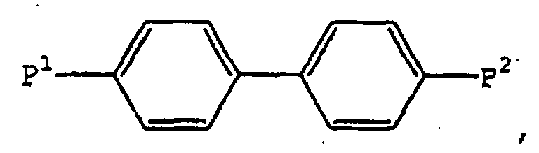
- the monomer compound for use in the present invention is preferably selected from those represented by the following general formula (1): P 1 -A 1 -(Z 1 -A 2 ) n -P 2 wherein P 1 and P 2 are functional groups and are independently selected from acrylate, methacrylate, vinyl, vinyloxy and epoxy groups, A 1 and A 2 are ring structures and independently selected from 1,4-phenylene and naphthalene-2,6-diyl groups, Z 1 represents a -COO- or a -OCO- group, or a single bond, and n is 0, 1 or 2.
- P 1 -A 1 -(Z 1 -A 2 ) n -P 2 wherein P 1 and P 2 are functional groups and are independently selected from acrylate, methacrylate, vinyl, vinyloxy and epoxy groups, A 1 and A 2 are ring structures and independently selected from 1,4-phenylene and naphthalene-2,6-diyl groups, Z 1 represents a -COO- or
- P 1 and P 2 are preferably acrylate groups, Z 1 is preferably a single bond, and n is preferably 0 or 1.
- the monomer for use in the present invention is more preferably a compound represented by any one of the following formulae: wherein P 1 and P 2 are as defined above in formula (1), particularly preferred being acrylate group.
- the compounds of formulae (1a) and (1b) are preferred, and the compound of formula (1a) is particularly preferred.
- a vertical alignment film was used in the liquid crystal display device. Also, a liquid crystal having a negative dielectric anisotropy was used and the director of liquid 'crystal molecules was set to be in the direction almost perpendicular to the substrate when a voltage was not applied.
- the polarizing plates were laminated on both sides of the liquid crystal display in the cross-nicol arrangement to give a normally black mode and the polarization axis of the polarizing plate was in parallel to the bus line.
- the panel size was 15 inches and the resolution was XGA.
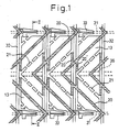
- Fig. 1 shows a schematic plan view illustrating the liquid display device produced
- Fig. 2 shows a cross-sectional view cut along the II-II line of Fig. 1.
- a black matrix 34 for shading and a color separation filter (color filter) 39 are formed on one glass substrate 16, and an ITO common electrode is formed on the entire surface of the color separation filter 39.
- protrusions 20 are further formed zigzag on the glass substrate 16, and auxiliary protrusions 20' are also formed.
- a plurality of parallel gate bus lines 31, a plurality of parallel data bus lines 32 formed in the direction perpendicular to the gate bus lines 31, thin-film transistors (TFTs) 33 formed like a matrix in correspondence to the intersection of the gate bus line 31 and the data bus line 32, and ITO display pixel electrodes 13 are provided.
- the gate bus line 31 is separated from the data bus line 32 by an insulating film 51, and source/drain electrodes of TFT 33 are formed in the same layer as the data bus line 32.
- An insulating film 52 is formed on the data bus line 32, and a pixel electrode 13 is further formed thereon. In the pixel electrode 13, as shown in the plan view of Fig.
- slits 21 are provided in parallel to protrusions 20 and at the middle position of adjacent protrusions 20.
- a Cs electrode 35 for auxiliary capacitance is provided at the middle position of adjacent gate bus lines 31 to run in parallel to the gate bus lines 31 so as to stabilize the potential of each pixel electrode 13.
- two glass substrates 16 and 17 are combined to oppose the common electrode 13 to the pixel electrodes 13, and a liquid crystal composition (not shown) is held therebetween.
- An alignment control film is formed on the surfaces of common electrode 12 and pixel electrodes 13, but for the sake of simplicity, these are not shown in Fig. 2.
- a polarizing plate laminated on each outer surface side of glass substrates 16 and 17 is not shown in Fig. 2.
- the 48-hour image burn percentage of this liquid crystal display device was 25%.
- the 48-hour image burn percentage of this liquid crystal display device was 26%
- the 48-hour image burn percentage of this liquid crystal display device was 6%.
- a liquid crystal display device greatly reduced in the image burn percentage can be provided.
Landscapes
- Chemical & Material Sciences (AREA)
- Physics & Mathematics (AREA)
- Crystallography & Structural Chemistry (AREA)
- Nonlinear Science (AREA)
- Organic Chemistry (AREA)
- Engineering & Computer Science (AREA)
- Materials Engineering (AREA)
- Optics & Photonics (AREA)
- General Physics & Mathematics (AREA)
- Mathematical Physics (AREA)
- Spectroscopy & Molecular Physics (AREA)
- Polymers & Plastics (AREA)
- Medicinal Chemistry (AREA)
- Chemical Kinetics & Catalysis (AREA)
- Health & Medical Sciences (AREA)
- Liquid Crystal (AREA)
- Addition Polymer Or Copolymer, Post-Treatments, Or Chemical Modifications (AREA)
- Liquid Crystal Substances (AREA)
- Polymerisation Methods In General (AREA)
Abstract
Description


Claims (10)
- A liquid crystal display device having two substrates each equipped with a transparent electrode and an alignment control film for aligning liquid crystal molecules, and comprising a liquid crystal composition between the substrates, the device being produced through the steps of injecting a polymerizable monomer-containing liquid crystal composition between the two substrates and while applying a voltage between the opposing transparent electrodes of the substrates, polymerizing said monomer,
wherein the polymerizable monomer contained in said liquid crystal composition has one or more ring or condensed ring structures and two functional groups bonded directly to said ring or condensed ring structure. - The liquid crystal display device as claimed in claim 1, wherein said monomer is represented by the following general formula:
- The liquid crystal display device as claimed in claim 2, wherein P1 and P2 are acrylate groups, Z1 is a single bond, and n is 0 or 1.
- The liquid crystal display device as claimed in claim 2, wherein said monomer is represented by the following formula:
 or
or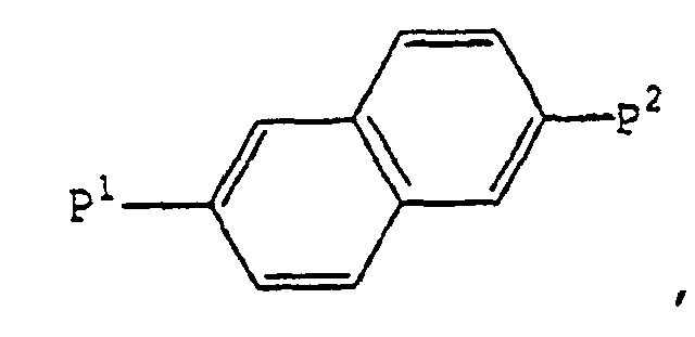 wherein P1 and P2 are independently selected from acrylate, methacrylate, vinyl, vinyloxy or epoxy groups.
- The liquid crystal display device as claimed in claim 2, wherein said monomer is represented by the following formula:or
 wherein P1 and P2 are independently selected from acrylate, methacrylate, vinyl, vinyloxy or epoxy groups.
- The liquid crystal display device as claimed in claim 2, wherein said monomer is represented by the following formula:wherein P1 and P2 are independently selected from acrylate, methacrylate, vinyl, vinyloxy or epoxy groups.

- The liquid crystal display device as claimed in any one of claims 4 to 6, wherein P1 and P2 are acrylate groups.
- The liquid crystal display device as claimed in claim 1, wherein said monomer is represented by the following formula:

- The liquid crystal display device as claimed in any one of claims 1 to 8, wherein said liquid crystal composition has a negative dielectric anisotropy.
- The liquid crystal display device as claimed in any one of claims 1 to 9, wherein the direction of liquid crystal molecules is a direction almost perpendicular to the substrate when a voltage is not applied.
Applications Claiming Priority (3)
| Application Number | Priority Date | Filing Date | Title |
|---|---|---|---|
| JP2002113972A JP4175826B2 (en) | 2002-04-16 | 2002-04-16 | Liquid crystal display |
| JP2002113972 | 2002-04-16 | ||
| PCT/JP2003/004791 WO2003087261A1 (en) | 2002-04-16 | 2003-04-15 | Liquid-crystal display |
Publications (3)
| Publication Number | Publication Date |
|---|---|
| EP1498468A1 true EP1498468A1 (en) | 2005-01-19 |
| EP1498468A4 EP1498468A4 (en) | 2007-03-28 |
| EP1498468B1 EP1498468B1 (en) | 2008-11-05 |
Family
ID=29243372
Family Applications (1)
| Application Number | Title | Priority Date | Filing Date |
|---|---|---|---|
| EP03746491A Expired - Lifetime EP1498468B1 (en) | 2002-04-16 | 2003-04-15 | Liquid-crystal display |
Country Status (9)
| Country | Link |
|---|---|
| US (1) | US7169449B2 (en) |
| EP (1) | EP1498468B1 (en) |
| JP (1) | JP4175826B2 (en) |
| KR (1) | KR100677804B1 (en) |
| CN (1) | CN1646662B (en) |
| AU (1) | AU2003235166A1 (en) |
| DE (1) | DE60324541D1 (en) |
| TW (1) | TWI321666B (en) |
| WO (1) | WO2003087261A1 (en) |
Cited By (29)
| Publication number | Priority date | Publication date | Assignee | Title |
|---|---|---|---|---|
| EP1889894A1 (en) | 2006-07-25 | 2008-02-20 | MERCK PATENT GmbH | Liquid crystalline medium |
| WO2009015744A1 (en) * | 2007-07-30 | 2009-02-05 | Merck Patent Gmbh | Liquid crystal display |
| DE102008036248A1 (en) | 2007-08-30 | 2009-03-05 | Merck Patent Gmbh | liquid-crystal display |
| DE102008035718A1 (en) | 2007-08-29 | 2009-03-05 | Merck Patent Gmbh | liquid-crystal display |
| WO2009030322A1 (en) * | 2007-08-30 | 2009-03-12 | Merck Patent Gmbh | Liquid crystal display |
| DE102008050375A1 (en) | 2007-10-22 | 2009-04-23 | Merck Patent Gmbh | Liquid crystalline medium |
| EP2065361A2 (en) | 2007-11-30 | 2009-06-03 | Merck Patent GmbH | Polymerisable compounds |
| WO2009118086A1 (en) * | 2008-03-25 | 2009-10-01 | Merck Patent Gmbh | Liquid crystal display |
| WO2010012363A1 (en) * | 2008-07-28 | 2010-02-04 | Merck Patent Gmbh | Liquid-crystal display |
| WO2010032946A2 (en) | 2008-09-17 | 2010-03-25 | Samsung Electronics Co., Ltd. | Alignment material, alignment layer, liquid crystal display device and manufacturing method thereof |
| DE102009043436A1 (en) | 2008-10-29 | 2010-05-06 | Merck Patent Gmbh | liquid-crystal display |
| DE102009055829A1 (en) | 2008-12-22 | 2010-06-24 | Merck Patent Gmbh | liquid-crystal display |
| WO2010105730A1 (en) | 2009-03-20 | 2010-09-23 | Merck Patent Gmbh | Polymers made of mixtures having vinyl ether monomers |
| EP2199362A3 (en) * | 2006-07-19 | 2010-10-13 | Merck Patent GmbH | Liquid crystalline medium |
| EP2243812A2 (en) | 2009-04-23 | 2010-10-27 | Merck Patent GmbH | Liquid crystal display |
| CN102395651A (en) * | 2009-04-14 | 2012-03-28 | Dic株式会社 | Liquid crystal composition containing polymerizable compound and liquid crystal display element using same |
| EP2416211A4 (en) * | 2009-03-30 | 2012-08-15 | Sharp Kk | Liquid crystal display device, process for producing liquid crystal display device, composition for forming polymer layer, and composition for forming liquid crystal layer |
| EP2330458A4 (en) * | 2008-09-03 | 2012-09-05 | Sharp Kk | Alignment film, alignment film material, liquid crystal display device comprising alignment film, and method for manufacturing same |
| US8274628B2 (en) | 2004-12-06 | 2012-09-25 | Semiconductor Energy Laboratory Co., Ltd. | Liquid crystal display device |
| DE102012004871A1 (en) | 2011-03-29 | 2012-10-04 | Merck Patent Gmbh | Liquid crystalline medium |
| EP2352061A4 (en) * | 2008-11-27 | 2013-07-10 | Sharp Kk | Orientation film, liquid crystal display having orientation film, and method for forming orientation film |
| US8514357B2 (en) | 2008-09-17 | 2013-08-20 | Samsung Display Co., Ltd. | Alignment material, alignment layer, liquid crystal display device and manufacturing method thereof |
| US8778466B2 (en) | 2006-10-12 | 2014-07-15 | Merck Patent Gmbh | Liquid-crystal display |
| KR20150035563A (en) | 2012-07-05 | 2015-04-06 | 제이엔씨 주식회사 | Polymerizable compound, liquid crystal composition, and liquid crystal display element |
| EP2952554A1 (en) * | 2010-12-24 | 2015-12-09 | DIC Corporation | Polymerizable compound-containing liquid crystal composition and liquid crystal display device using the same |
| EP3103855A1 (en) | 2015-06-11 | 2016-12-14 | Merck Patent GmbH | Liquid-crystalline medium |
| US9557605B2 (en) | 2010-10-14 | 2017-01-31 | Merck Patent Gmbh | Method of producing liquid crystal display device |
| EP2597134A3 (en) * | 2011-11-23 | 2017-08-09 | Samsung Display Co., Ltd. | Alignment layer, liquid crystal display device, and method for manufacturing the same |
| US9798179B2 (en) | 2010-10-14 | 2017-10-24 | Merck Patent Gmbh | Liquid crystal display device |
Families Citing this family (247)
| Publication number | Priority date | Publication date | Assignee | Title |
|---|---|---|---|---|
| JP2005173439A (en) | 2003-12-15 | 2005-06-30 | Fujitsu Display Technologies Corp | Liquid crystal display device and manufacturing method thereof |
| JP4372648B2 (en) | 2004-09-13 | 2009-11-25 | シャープ株式会社 | Liquid crystal display device and manufacturing method thereof |
| JP4549819B2 (en) * | 2004-11-12 | 2010-09-22 | シャープ株式会社 | Liquid crystal display device and manufacturing method thereof |
| JP5238127B2 (en) * | 2004-12-06 | 2013-07-17 | 株式会社半導体エネルギー研究所 | Liquid crystal display |
| JP4628802B2 (en) * | 2005-01-20 | 2011-02-09 | シャープ株式会社 | Liquid crystal display |
| JP4753001B2 (en) * | 2005-02-02 | 2011-08-17 | Jsr株式会社 | Liquid crystal alignment film, liquid crystal display element and manufacturing method thereof |
| TWI325982B (en) * | 2005-06-08 | 2010-06-11 | Au Optronics Corp | Method for fabricating liquid crystal display |
| CN100572351C (en) * | 2006-08-11 | 2009-12-23 | 友达光电股份有限公司 | Monomer and method for manufacturing liquid crystal display panel by using same |
| TWI354677B (en) * | 2007-01-31 | 2011-12-21 | Au Optronics Corp | Photosensitive monomer, liquid crystal material ha |
| TWI349029B (en) * | 2007-03-30 | 2011-09-21 | Au Optronics Corp | Liquid crystalline medium, liquid crystal display panel using the same, and method for manufacturing liquid crystal display panel |
| KR101437864B1 (en) | 2007-04-24 | 2014-11-03 | 삼성디스플레이 주식회사 | Liquid crystal display and method for manufacturing the same |
| JP2010276622A (en) | 2007-09-19 | 2010-12-09 | シャープ株式会社 | Liquid crystal display |
| JP2009092816A (en) * | 2007-10-05 | 2009-04-30 | Sony Corp | Manufacturing method of liquid crystal display element |
| JP5000722B2 (en) | 2007-10-15 | 2012-08-15 | シャープ株式会社 | Liquid crystal display |
| TWI336017B (en) * | 2007-10-24 | 2011-01-11 | Au Optronics Corp | Method for manufacturing liquid crystal display |
| TWI368645B (en) * | 2007-10-24 | 2012-07-21 | Au Optronics Corp | Liquid crystal medium for psa process and liquid crystal display device |
| US8283000B2 (en) | 2008-02-22 | 2012-10-09 | Adeka Corporation | Liquid crystal composition containing polymerizable compound and liquid crystal display using the liquid crystal composition |
| JP4618321B2 (en) * | 2008-04-24 | 2011-01-26 | ソニー株式会社 | Liquid crystal display element |
| US20110122350A1 (en) * | 2008-05-12 | 2011-05-26 | Kunihiro Tashiro | Liquid crystal display device |
| TWI395993B (en) * | 2008-06-30 | 2013-05-11 | Au Optronics Corp | Liquid crystal display panel and composition of liquid crystal layer thereof |
| CN101320153B (en) * | 2008-07-08 | 2010-10-13 | 友达光电股份有限公司 | Liquid crystal display panel and liquid crystal material thereof |
| US8436971B2 (en) | 2008-07-15 | 2013-05-07 | Sharp Kabushiki Kaisha | Liquid crystal display device |
| CN102112911B (en) * | 2008-08-05 | 2014-05-07 | 夏普株式会社 | Liquid crystal display device and method for manufacturing the same |
| KR101499238B1 (en) * | 2008-08-07 | 2015-03-05 | 삼성디스플레이 주식회사 | Liquid crystal display |
| WO2010023880A1 (en) * | 2008-08-27 | 2010-03-04 | シャープ株式会社 | Liquid crystal display device |
| TWI395012B (en) * | 2008-09-03 | 2013-05-01 | Au Optronics Corp | Liquid crystal display panel and method for manufacturing the same |
| US20110216262A1 (en) * | 2008-11-11 | 2011-09-08 | Hisashi Nagata | Liquid crystal display device and method for manufacturing liquid crystal display device |
| CN102224450B (en) * | 2008-11-27 | 2014-10-08 | 夏普株式会社 | Liquid crystal display and method for producing the same |
| EP3075816B1 (en) | 2009-01-22 | 2018-05-23 | JNC Corporation | Liquid crystal composition and liquid crystal display device |
| TWI388905B (en) * | 2009-03-17 | 2013-03-11 | Au Optronics Corp | Liquid crystal display panel and method for fabricating the same |
| JPWO2010116565A1 (en) | 2009-04-08 | 2012-10-18 | シャープ株式会社 | Liquid crystal display device, method for manufacturing liquid crystal display device, composition for forming photopolymer film, and composition for forming liquid crystal layer |
| TWI458706B (en) | 2009-05-11 | 2014-11-01 | Jnc Corp | Polymerizable compound and liquid crystal composition containing the same |
| DE102009022309A1 (en) | 2009-05-22 | 2010-11-25 | Merck Patent Gmbh | liquid-crystal display |
| KR101641535B1 (en) * | 2009-06-01 | 2016-07-22 | 삼성디스플레이 주식회사 | Method of manufacturing a liquid crystal display panel and liquid crystal display panel |
| US8455062B2 (en) | 2009-07-08 | 2013-06-04 | Sharp Kabushiki Kaisha | Liquid crystal display panel and process for production thereof |
| EP2463709A4 (en) | 2009-07-08 | 2014-01-22 | Sharp Kk | Liquid crystal display panel and process for production thereof |
| TWI490316B (en) * | 2009-07-09 | 2015-07-01 | Rolic Ag | Ester group containing liquid crystals for optical or electro optical devices |
| KR101615926B1 (en) | 2009-07-28 | 2016-04-28 | 삼성디스플레이 주식회사 | Liquid crystal display device and method of manufacturing the same |
| JP5621966B2 (en) * | 2009-09-02 | 2014-11-12 | Jsr株式会社 | Manufacturing method of liquid crystal display element |
| EP2292720A1 (en) | 2009-09-08 | 2011-03-09 | Merck Patent GmbH | Liquid-crystal display |
| WO2011032630A1 (en) | 2009-09-18 | 2011-03-24 | Merck Patent Gmbh | Polymerizable compounds and liquid crystal media |
| DE102010035730A1 (en) | 2009-09-28 | 2011-04-07 | Merck Patent Gmbh | Polymerizable compounds and their use in liquid crystal displays |
| TWI477589B (en) | 2009-10-13 | 2015-03-21 | Dainippon Ink & Chemicals | Polymerizable compounds |
| DE102010047409A1 (en) | 2009-10-28 | 2011-05-05 | Merck Patent Gmbh | Polymerizable compounds and their use in liquid crystal displays |
| US8741397B2 (en) | 2009-11-09 | 2014-06-03 | Jnc Corporation | Liquid crystal display element, liquid crystal composition, aligning agent, method for producing liquid crystal display element, and use of liquid crystal composition |
| EP2502973A4 (en) | 2009-11-18 | 2014-07-23 | Adeka Corp | LIQUID CRYSTAL COMPOSITION CONTAINING POLYMERIZABLE COMPOUND, AND LIQUID CRYSTAL DISPLAY ELEMENT USING SAID LIQUID CRYSTAL COMPOSITION |
| JP4840543B2 (en) | 2009-12-14 | 2011-12-21 | Dic株式会社 | Polymerizable compound-containing liquid crystal composition and liquid crystal display device using the same |
| KR101663563B1 (en) * | 2009-12-24 | 2016-10-07 | 엘지디스플레이 주식회사 | Methode of fabricating liquid crystal display device |
| WO2011088882A1 (en) | 2010-01-21 | 2011-07-28 | Merck Patent Gmbh | Polymerizable compounds and liquid crystal media |
| JP5720919B2 (en) | 2010-02-04 | 2015-05-20 | Dic株式会社 | Liquid crystal composition containing polymerizable compound and liquid crystal display device using the same |
| JP5257548B2 (en) | 2010-02-26 | 2013-08-07 | 日産化学工業株式会社 | Liquid crystal display element and liquid crystal aligning agent |
| DE102011011836A1 (en) | 2010-03-09 | 2011-09-15 | Merck Patent Gmbh | Polymerizable compounds and their use in liquid crystal media and liquid crystal displays |
| JP5692565B2 (en) | 2010-04-16 | 2015-04-01 | Dic株式会社 | Liquid crystal composition containing polymerizable compound and liquid crystal display device using the same |
| JP5743129B2 (en) | 2010-04-16 | 2015-07-01 | Dic株式会社 | Liquid crystal composition containing polymerizable compound and liquid crystal display device using the same |
| DE102011015546A1 (en) | 2010-04-26 | 2012-01-26 | Merck Patent Gmbh | Polymerizable compounds and their use in liquid crystal media and liquid crystal displays |
| JP5729382B2 (en) | 2010-05-10 | 2015-06-03 | Jnc株式会社 | Polymerizable compound |
| CN102279487B (en) * | 2010-06-10 | 2013-08-07 | 统炀企业有限公司 | Method for forming liquid crystal alignment layer by photopolymerization |
| JP5694525B2 (en) | 2010-06-25 | 2015-04-01 | メルク パテント ゲゼルシャフト ミット ベシュレンクテル ハフツングMerck Patent Gesellschaft mit beschraenkter Haftung | Polymerizable compounds and their use in liquid crystal displays |
| US9045683B2 (en) | 2010-06-25 | 2015-06-02 | Merck Patent Gmbh | Polymerizable compounds and use thereof in liquid crystal displays |
| WO2012002511A1 (en) | 2010-06-30 | 2012-01-05 | 日産化学工業株式会社 | Liquid crystal-aligning agent, liquid crystal-aligning film, liquid crystal display element and method for producing liquid crystal display elements |
| TWI520948B (en) | 2010-06-30 | 2016-02-11 | Nissan Chemical Ind Ltd | A liquid crystal alignment device, a liquid crystal alignment device, a liquid crystal display device, and a liquid crystal display device, and a polymerizable compound |
| JP5776908B2 (en) * | 2010-06-30 | 2015-09-09 | 日産化学工業株式会社 | Liquid crystal aligning agent, liquid crystal alignment film, liquid crystal display element, and method for manufacturing liquid crystal display element |
| DE102011105936A1 (en) | 2010-07-15 | 2012-01-19 | Merck Patent Gmbh | Liquid-crystalline media and liquid crystal displays with polymer-stabilized homeotropic alignment |
| DE102011105930A1 (en) | 2010-07-21 | 2012-01-26 | Merck Patent Gmbh | Polymerizable mixtures and their use in liquid crystal displays |
| JP5951936B2 (en) | 2010-07-21 | 2016-07-13 | Jsr株式会社 | Manufacturing method of liquid crystal display element |
| EP2596082B1 (en) | 2010-07-22 | 2015-11-04 | Merck Patent GmbH | Polymer-stabilized liquid-crystal media and displays |
| WO2012017884A1 (en) | 2010-08-03 | 2012-02-09 | シャープ株式会社 | Liquid crystal display device and process for producing liquid crystal display device |
| WO2012017883A1 (en) | 2010-08-03 | 2012-02-09 | シャープ株式会社 | Liquid crystal display device and liquid crystal display device manufacturing method |
| US9164325B2 (en) | 2010-08-03 | 2015-10-20 | Sharp Kabushiki Kaisha | Liquid crystal display device and process for producing liquid crystal display device |
| CN101916012B (en) * | 2010-08-04 | 2011-10-12 | 友达光电股份有限公司 | display panel |
| EP2606101B1 (en) * | 2010-08-19 | 2016-06-08 | Merck Patent GmbH | Liquid crystal medium and liquid crystal displays |
| US9644146B2 (en) | 2010-09-07 | 2017-05-09 | Sharp Kabushiki Kaisha | Composition for forming liquid crystal layer, liquid crystal display device, and method for producing liquid crystal display device |
| DE102011108708A1 (en) | 2010-09-25 | 2012-03-29 | Merck Patent Gmbh | Liquid crystal displays and liquid crystal media with homeotropic alignment |
| KR20120042169A (en) | 2010-10-22 | 2012-05-03 | 삼성모바일디스플레이주식회사 | Liquid crystal display and manufacturing method of the same |
| WO2012055473A1 (en) | 2010-10-26 | 2012-05-03 | Merck Patent Gmbh | Liquid-crystal medium and process for preparing a liquid-crystal device |
| US9182632B2 (en) | 2010-12-06 | 2015-11-10 | Sharp Kabushiki Kaisha | Liquid crystal display device and method for manufacturing liquid crystal display device |
| US9239493B2 (en) | 2010-12-22 | 2016-01-19 | Sharp Kabushiki Kaisha | Liquid crystal alignment agent, liquid crystal display, and method for manufacturing liquid crystal display |
| EP2665798B1 (en) | 2011-01-20 | 2014-10-08 | Merck Patent GmbH | Polymerisable compounds and the use thereof in liquid-crystal displays |
| US9249355B2 (en) | 2011-02-05 | 2016-02-02 | Merck Patent Gmbh | Liquid-crystal displays having homeotropic alignment |
| CN104910922A (en) | 2011-03-09 | 2015-09-16 | 夏普株式会社 | Liquid crystal composition and liquid crystal display device |
| JP5966329B2 (en) * | 2011-03-30 | 2016-08-10 | Jsr株式会社 | Manufacturing method of liquid crystal display element |
| CN103562782B (en) | 2011-03-31 | 2016-06-15 | 日产化学工业株式会社 | The manufacture method of aligning agent for liquid crystal, liquid crystal orientation film, liquid crystal display cells and liquid crystal display cells |
| KR20120124012A (en) | 2011-05-02 | 2012-11-12 | 삼성디스플레이 주식회사 | Liquid crystal display |
| JP5834489B2 (en) * | 2011-05-18 | 2015-12-24 | Dic株式会社 | Polymerizable naphthalene compound |
| JP5678798B2 (en) * | 2011-05-20 | 2015-03-04 | Dic株式会社 | Polymerizable compound-containing liquid crystal composition and liquid crystal display device using the same |
| JP5779977B2 (en) | 2011-05-20 | 2015-09-16 | Dic株式会社 | Nematic liquid crystal composition and liquid crystal display device using the same |
| EP2714844B1 (en) | 2011-05-27 | 2016-12-28 | Merck Patent GmbH | Polymerizable compounds and their use in liquid crystal media and liquid crystal displays |
| WO2013002084A1 (en) * | 2011-06-27 | 2013-01-03 | シャープ株式会社 | Liquid crystal display device and method for manufacturing liquid crystal display device |
| US9217897B2 (en) | 2011-07-14 | 2015-12-22 | Sharp Kabushiki Kaisha | Liquid crystal display device and method for manufacturing liquid crystal display device |
| KR101978993B1 (en) | 2011-08-11 | 2019-08-28 | 디아이씨 가부시끼가이샤 | Liquid crystal composition containing polymerizable compound and liquid crystal display device using same |
| KR20130017938A (en) * | 2011-08-12 | 2013-02-20 | 주식회사 동진쎄미켐 | Reactive liquid crystal composition |
| WO2013027548A1 (en) | 2011-08-25 | 2013-02-28 | シャープ株式会社 | Method for manufacturing liquid crystal display device |
| CN103748508B (en) | 2011-08-26 | 2016-08-31 | 夏普株式会社 | Liquid crystal display panel and liquid crystal display device |
| CN103782230B (en) | 2011-08-29 | 2017-03-01 | 夏普株式会社 | Method for manufacturing liquid crystal display device |
| CN103797407B (en) | 2011-08-29 | 2016-07-06 | 夏普株式会社 | The manufacture method of liquid crystal indicator |
| US9073850B2 (en) | 2011-11-24 | 2015-07-07 | Jnc Corporation | Polymerizable compound |
| US9074132B2 (en) | 2011-11-28 | 2015-07-07 | Jnc Corporation | Liquid crystal composition and liquid crystal display device |
| WO2013099937A1 (en) | 2011-12-28 | 2013-07-04 | 日産化学工業株式会社 | Liquid crystal aligning agent, liquid crystal alignment membrane, liquid crystal display element, and method for manufacturing liquid crystal display element |
| JP6146578B2 (en) | 2011-12-28 | 2017-06-14 | 日産化学工業株式会社 | Liquid crystal aligning agent, liquid crystal alignment film, liquid crystal display element, and method for manufacturing liquid crystal display element |
| JP6146577B2 (en) | 2011-12-28 | 2017-06-14 | 日産化学工業株式会社 | Liquid crystal alignment agent, liquid crystal alignment film, and liquid crystal display element |
| US9733524B2 (en) | 2012-01-30 | 2017-08-15 | Sharp Kabushiki Kaisha | Liquid crystal display device and manufacturing method therefor |
| TWI452122B (en) | 2012-02-24 | 2014-09-11 | Dainippon Ink & Chemicals | Liquid crystal composition |
| JP2015099170A (en) * | 2012-03-05 | 2015-05-28 | シャープ株式会社 | Liquid crystal display device and method for manufacturing liquid crystal display device |
| DE102012205373A1 (en) | 2012-04-02 | 2013-10-02 | Kyocera Display Europe Gmbh | Method for manufacturing LCD, involves combining inner and rough surface of substrate to achieve perpendicular orientation of liquid crystal with multiple angles |
| US9157027B2 (en) | 2012-04-24 | 2015-10-13 | Jnc Corporation | Compound having four polymerizable groups, liquid crystal composition and liquid crystal display device |
| WO2013161865A1 (en) | 2012-04-27 | 2013-10-31 | シャープ株式会社 | Liquid crystal display device and method for manufacturing liquid crystal display device |
| CN102660300B (en) | 2012-04-28 | 2014-02-12 | 深圳市华星光电技术有限公司 | Liquid crystal medium composition, liquid crystal display using same and manufacturing method thereof |
| KR102113052B1 (en) | 2012-06-02 | 2020-05-20 | 메르크 파텐트 게엠베하 | Liquid crystal medium |
| EP2682448B1 (en) | 2012-07-05 | 2016-04-20 | Merck Patent GmbH | Polymerisable compounds and the use thereof in liquid-crystal displays |
| US9150787B2 (en) | 2012-07-06 | 2015-10-06 | Jnc Corporation | Liquid crystal composition and liquid crystal display device |
| CN102863970A (en) * | 2012-09-21 | 2013-01-09 | 深圳市华星光电技术有限公司 | Liquid-crystal medium mixture and liquid-crystal display utilizing same |
| CN102863968A (en) * | 2012-09-21 | 2013-01-09 | 深圳市华星光电技术有限公司 | Liquid crystal medium mixture and liquid crystal display using liquid crystal medium mixture |
| CN104662469B (en) | 2012-09-24 | 2018-09-11 | 夏普株式会社 | Liquid crystal disply device and its preparation method |
| WO2014061756A1 (en) | 2012-10-19 | 2014-04-24 | シャープ株式会社 | Monomer, liquid crystal composition, liquid crystal display device, and production method for liquid crystal display device |
| US9983441B2 (en) | 2012-10-19 | 2018-05-29 | Merck Patent Gmbh | Liquid crystal display device |
| US10550327B2 (en) | 2012-11-21 | 2020-02-04 | Merck Patent Gmbh | Polymerisable compounds and the use thereof in liquid-crystal displays |
| KR20150100766A (en) | 2012-12-17 | 2015-09-02 | 메르크 파텐트 게엠베하 | Liquid-crystal displays and liquid-crystalline media having homeotropic alignment |
| KR102168590B1 (en) | 2013-03-08 | 2020-10-21 | 닛산 가가쿠 가부시키가이샤 | Liquid crystal aligning agent, liquid crystal display element obtained using same, and method for manufacturing said liquid crystal display element |
| KR102114521B1 (en) | 2013-03-12 | 2020-05-22 | 닛산 가가쿠 가부시키가이샤 | Liquid crystal aligning agent containing crosslinkable compound having photoreactive group |
| US9725651B2 (en) | 2013-03-21 | 2017-08-08 | Dic Corporation | Polymerizable compound-containing liquid crystal composition and liquid crystal display element using same |
| US9777218B2 (en) | 2013-03-25 | 2017-10-03 | Dic Corporation | Liquid crystal display element |
| JP6102423B2 (en) * | 2013-03-29 | 2017-03-29 | Dic株式会社 | Polymerizable compound and optical element |
| JP6398973B2 (en) | 2013-06-06 | 2018-10-03 | 日産化学株式会社 | Liquid crystal alignment agent, liquid crystal alignment film, and liquid crystal display element |
| EP2818531B1 (en) | 2013-06-25 | 2017-07-26 | Merck Patent GmbH | Polymerisable compounds and the use thereof in liquid-crystal displays |
| TWI642725B (en) | 2013-06-25 | 2018-12-01 | 日產化學工業股份有限公司 | Liquid crystal alignment agent, liquid crystal alignment film, liquid crystal display element |
| CN105358655B (en) | 2013-07-11 | 2017-05-17 | 捷恩智株式会社 | Liquid crystal composition and liquid crystal display element |
| JP6561833B2 (en) | 2013-09-03 | 2019-08-21 | 日産化学株式会社 | Liquid crystal alignment agent, liquid crystal alignment film, and liquid crystal display element |
| EP2848676B1 (en) | 2013-09-12 | 2017-07-26 | Merck Patent GmbH | Liquid crystal medium |
| US10377949B2 (en) | 2013-10-22 | 2019-08-13 | Jnc Corporation | Liquid crystal composition and liquid crystal display device |
| JP2015110741A (en) | 2013-11-11 | 2015-06-18 | Jnc株式会社 | Liquid crystal composition and liquid crystal display element |
| WO2015087911A1 (en) * | 2013-12-13 | 2015-06-18 | シャープ株式会社 | Light modulation device and display device |
| TWI657297B (en) | 2014-01-30 | 2019-04-21 | 日商日產化學工業股份有限公司 | Liquid crystal alignment agent, liquid crystal alignment film, and liquid crystal display element |
| JP6807640B2 (en) | 2014-01-30 | 2021-01-06 | 日産化学株式会社 | Polymerizable compound substituted with halogen atom |
| EP3730590B1 (en) | 2014-03-10 | 2025-12-24 | Merck Patent GmbH | Liquid crystal media with homeotropic alignment |
| EP2921545B1 (en) | 2014-03-21 | 2019-08-21 | Merck Patent GmbH | Polymerisable compounds and the use thereof in liquid-crystal displays |
| JP2015205982A (en) | 2014-04-18 | 2015-11-19 | Jnc株式会社 | Liquid crystal composition and liquid crystal display element |
| US10351772B2 (en) | 2014-05-13 | 2019-07-16 | Dic Corporation | Nematic liquid crystal composition and liquid crystal display element using same |
| CN106459764A (en) | 2014-06-19 | 2017-02-22 | Dic株式会社 | Liquid crystal composition containing polymerizable monomer and liquid crystal display element using same |
| US10294426B2 (en) | 2014-07-28 | 2019-05-21 | Merck Patent Gmbh | Liquid crystalline media having homeotropic alignment |
| EP3124465B1 (en) | 2014-07-30 | 2022-09-28 | Merck Patent GmbH | Polymerisable compounds and the use thereof in liquid-crystal displays |
| JP6451549B2 (en) * | 2014-08-11 | 2019-01-16 | Jnc株式会社 | Polymerizable compound and liquid crystal display device |
| EP2990459B1 (en) | 2014-08-25 | 2017-04-26 | Merck Patent GmbH | Polymerisable compounds and the use thereof in liquid-crystal displays |
| EP3372655B1 (en) | 2014-08-25 | 2019-12-18 | Merck Patent GmbH | Liquid-crystal medium |
| WO2016035786A1 (en) | 2014-09-05 | 2016-03-10 | Dic株式会社 | Nematic liquid crystal composition, and liquid crystal display element using same |
| US9659965B2 (en) | 2014-09-12 | 2017-05-23 | Samsung Display Co., Ltd. | Liquid crystal display device and method of manufacturing the same |
| KR20160035173A (en) | 2014-09-22 | 2016-03-31 | 삼성디스플레이 주식회사 | Liquid crystalline compound, liquid crystalline composition comprising the same and liquid crystalline display comprising the same |
| CN107108540B (en) | 2014-11-04 | 2019-08-02 | 日产化学工业株式会社 | Butyrolactone compound and method of manufacture |
| JP6733550B2 (en) | 2014-11-04 | 2020-08-05 | 日産化学株式会社 | Method for producing butyrolactone compound |
| TW202244246A (en) | 2014-11-06 | 2022-11-16 | 公立大學法人兵庫縣立大學 | Photoreactive liquid crystal composition light control element and method for producing light control element |
| EP3020785B1 (en) | 2014-11-14 | 2017-12-13 | Merck Patent GmbH | Liquid crystal medium |
| EP3029127B1 (en) | 2014-12-01 | 2017-12-20 | Merck Patent GmbH | Liquid crystal medium |
| WO2016104165A1 (en) | 2014-12-25 | 2016-06-30 | Dic株式会社 | Nematic liquid crystal composition and liquid crystal display element using same |
| JP6733552B2 (en) | 2015-01-13 | 2020-08-05 | 日産化学株式会社 | Method for producing diamine precursor compound |
| EP3048159B1 (en) | 2015-01-22 | 2019-08-07 | Merck Patent GmbH | Liquid crystal medium |
| WO2016125871A1 (en) | 2015-02-06 | 2016-08-11 | 日産化学工業株式会社 | Liquid crystal orientation agent, liquid crystal oriented film, and liquid crystal display element |
| WO2016125870A1 (en) | 2015-02-06 | 2016-08-11 | 日産化学工業株式会社 | Liquid crystal orienting agent, liquid crystal display element, and method for producing liquid crystal display element |
| CN107533260B (en) | 2015-03-04 | 2020-12-25 | 日产化学工业株式会社 | Liquid crystal aligning agent, liquid crystal alignment film, and liquid crystal display element |
| WO2016140302A1 (en) | 2015-03-04 | 2016-09-09 | 日産化学工業株式会社 | Polyimide precursor, and liquid crystal alignment agent, liquid crystal alignment film, and liquid crystal display element having precursor |
| CN107533259B (en) | 2015-03-04 | 2024-06-21 | 日产化学工业株式会社 | Liquid crystal alignment agent, liquid crystal alignment film, and liquid crystal display element |
| KR20160129998A (en) | 2015-04-30 | 2016-11-10 | 삼성디스플레이 주식회사 | Display device and manufacturing method thereof |
| EP3121247B1 (en) | 2015-06-09 | 2019-10-02 | Merck Patent GmbH | Polymerisable compounds and the use thereof in liquid-crystal displays |
| EP3112440B1 (en) | 2015-07-02 | 2019-07-24 | Merck Patent GmbH | Liquid-crystal medium |
| KR102573450B1 (en) | 2015-08-19 | 2023-08-31 | 닛산 가가쿠 가부시키가이샤 | Novel imide-based polymers used in liquid crystal alignment agents, etc. |
| CN108139634B (en) | 2015-08-19 | 2021-07-09 | 日产化学工业株式会社 | Liquid crystal aligning agent, liquid crystal aligning film, and liquid crystal display element |
| WO2017038627A1 (en) | 2015-08-28 | 2017-03-09 | 日産化学工業株式会社 | Novel diamine compound having radical generation ability and base generation ability, and novel imide polymer using said novel diamine compound as starting material |
| JP2018533072A (en) | 2015-10-23 | 2018-11-08 | メルク パテント ゲゼルシャフト ミット ベシュレンクテル ハフツングMerck Patent Gesellschaft mit beschraenkter Haftung | Benzyl monoketals and their use |
| EP3162875B1 (en) | 2015-10-30 | 2018-05-23 | Merck Patent GmbH | Polymerisable compounds and the use thereof in liquid-crystal displays |
| JP2019505496A (en) | 2015-12-17 | 2019-02-28 | メルク・パテント・ゲゼルシヤフト・ミツト・ベシユレンクテル・ハフツングMerck Patent GmbH | Cinnamic acid derivatives |
| US10877304B2 (en) | 2016-01-07 | 2020-12-29 | Sharp Kabushiki Kaisha | Liquid crystal display device and method for manufacturing liquid crystal display device |
| US10047290B2 (en) | 2016-02-05 | 2018-08-14 | Jnc Corporation | Liquid crystal composition and liquid crystal display device |
| CN108473872B (en) | 2016-04-27 | 2022-08-02 | Dic株式会社 | Liquid crystal composition and liquid crystal display element |
| WO2017188001A1 (en) | 2016-04-27 | 2017-11-02 | Dic株式会社 | Polymerizable compound and liquid crystal composition using same |
| TWI744302B (en) | 2016-05-19 | 2021-11-01 | 日商捷恩智股份有限公司 | Polymerizable composition, liquid crystal composite, optical anisotropic body, liquid crystal display and use thereof |
| CN109564369B (en) | 2016-06-14 | 2022-08-26 | 日产化学株式会社 | Liquid crystal aligning agent, liquid crystal alignment film, and liquid crystal display element |
| US11299673B2 (en) | 2016-08-12 | 2022-04-12 | Merck Patent Gmbh | Liquid-crystal medium |
| KR102662829B1 (en) | 2016-09-27 | 2024-05-03 | 티씨엘 차이나 스타 옵토일렉트로닉스 테크놀로지 컴퍼니 리미티드 | Liquid crystal composition and display device including the same |
| DE102017010159A1 (en) | 2016-11-21 | 2018-05-24 | Merck Patent Gmbh | Compounds for homeotropic alignment of liquid-crystalline media |
| WO2018097155A1 (en) | 2016-11-22 | 2018-05-31 | 日産化学工業株式会社 | Method for manufacturing liquid crystal display element, substrate for liquid crystal display element, and liquid crystal display element assembly |
| KR102538719B1 (en) | 2016-12-08 | 2023-06-01 | 메르크 파텐트 게엠베하 | Polymerisable compounds and the use thereof in liquid-crystal displays |
| WO2018110531A1 (en) | 2016-12-15 | 2018-06-21 | Dic株式会社 | Liquid crystal display element |
| CN110573952B (en) | 2017-03-02 | 2022-03-22 | 日产化学株式会社 | Liquid crystal aligning agent, liquid crystal aligning film, and liquid crystal display element |
| US11718791B2 (en) | 2017-03-09 | 2023-08-08 | Merck Patent Gmbh | Polymerisable compounds and the use thereof in liquid-crystal displays |
| TWI755503B (en) | 2017-03-30 | 2022-02-21 | 日商迪愛生股份有限公司 | Manufacturing method of liquid crystal display element |
| JP7161147B2 (en) | 2017-06-14 | 2022-10-26 | 日産化学株式会社 | Liquid crystal alignment agent, liquid crystal alignment film, liquid crystal display element using the same, and method for producing the liquid crystal alignment film |
| CN109207169B (en) | 2017-06-30 | 2022-02-22 | 江苏和成显示科技有限公司 | Liquid crystal composition and application thereof |
| WO2019013339A1 (en) | 2017-07-14 | 2019-01-17 | 日産化学株式会社 | Liquid crystal alignment agent, liquid crystal alignment film, and liquid crystal display element using same |
| KR102456697B1 (en) | 2017-08-22 | 2022-10-19 | 삼성디스플레이 주식회사 | Liquid crystal display and manufacturing method thereof |
| JP7255486B2 (en) | 2017-09-13 | 2023-04-11 | 日産化学株式会社 | Liquid crystal alignment agent, liquid crystal alignment film and liquid crystal display element |
| CN111148819B (en) | 2017-09-29 | 2023-06-16 | 默克专利股份有限公司 | Polymerizable compounds and their use in liquid crystal displays |
| EP3502210B1 (en) | 2017-12-20 | 2020-09-09 | Merck Patent GmbH | Liquid-crystal medium |
| EP3502209B1 (en) | 2017-12-20 | 2020-10-14 | Merck Patent GmbH | Liquid-crystalline media having homeotropic alignment |
| DE102019000286A1 (en) | 2018-02-05 | 2019-08-08 | Merck Patent Gmbh | Compounds for homeotropic alignment of liquid-crystalline media |
| KR102953188B1 (en) | 2018-02-23 | 2026-04-15 | 닛산 가가쿠 가부시키가이샤 | Method for manufacturing a liquid crystal display element |
| CN111712557A (en) | 2018-03-30 | 2020-09-25 | 捷恩智株式会社 | Liquid crystal composition and liquid crystal display element |
| WO2019206788A1 (en) | 2018-04-23 | 2019-10-31 | Merck Patent Gmbh | Liquid crystal mixture and liquid crystal display |
| KR20210005122A (en) | 2018-04-23 | 2021-01-13 | 메르크 파텐트 게엠베하 | Liquid crystal mixture and liquid crystal display |
| WO2019206789A1 (en) | 2018-04-23 | 2019-10-31 | Merck Patent Gmbh | Liquid crystal mixture and liquid crystal display |
| WO2019206791A1 (en) | 2018-04-23 | 2019-10-31 | Merck Patent Gmbh | Liquid crystal mixture and liquid crystal display |
| CN108681158B (en) * | 2018-05-21 | 2021-12-03 | 南京京东方显示技术有限公司 | Self-alignment display device and alignment method thereof |
| JP2019211719A (en) * | 2018-06-08 | 2019-12-12 | Jnc株式会社 | Liquid crystal element with insulating film, light control window, and manufacturing method |
| KR102744958B1 (en) | 2018-06-19 | 2024-12-19 | 닛산 가가쿠 가부시키가이샤 | Liquid crystal alignment agent, liquid crystal alignment film and liquid crystal display element using the same and method for manufacturing the liquid crystal display element, diamine compound |
| EP3604481B1 (en) | 2018-07-31 | 2021-05-26 | Merck Patent GmbH | Liquid-crystal medium |
| WO2020038859A1 (en) | 2018-08-22 | 2020-02-27 | Merck Patent Gmbh | Liquid crystal mixture and liquid crystal display |
| WO2020038861A1 (en) | 2018-08-22 | 2020-02-27 | Merck Patent Gmbh | Liquid crystal mixture and liquid crystal display |
| WO2020043643A1 (en) | 2018-08-28 | 2020-03-05 | Merck Patent Gmbh | Liquid crystal mixture and liquid crystal display |
| EP3789470A1 (en) | 2018-09-06 | 2021-03-10 | Merck Patent GmbH | Liquid crystal media comprising polymerisable compounds |
| EP3847224B1 (en) | 2018-09-06 | 2025-08-06 | Merck Patent GmbH | Polymerisable compounds and the use thereof in liquid-crystal displays |
| EP4209567B1 (en) | 2018-09-27 | 2024-08-14 | Merck Patent GmbH | Liquid-crystal medium |
| US20220106525A1 (en) | 2018-10-10 | 2022-04-07 | Merck Patent Gmbh | Liquid crystal mixture and liquid crystal display |
| EP3816264A1 (en) | 2018-10-31 | 2021-05-05 | Merck Patent GmbH | Liquid crystal media comprising polymerisable compounds |
| EP3877485B1 (en) | 2018-11-07 | 2023-09-06 | Merck Patent GmbH | Liquid crystal media comprising polymerisable compounds |
| US11999891B2 (en) | 2018-12-07 | 2024-06-04 | Merck Patent Gmbh | Liquid-crystal medium comprising polymerisable compounds and the use thereof in liquid-crystal displays |
| US11739266B2 (en) | 2018-12-07 | 2023-08-29 | Merck Patent Gmbh | Polymerisable compounds and the use thereof in liquid-crystal displays |
| US20230068853A1 (en) | 2018-12-12 | 2023-03-02 | Merck Patent Gmbh | Liquid crystal mixture and liquid crystal display |
| US11873438B2 (en) | 2018-12-20 | 2024-01-16 | Merck Patent Gmbh | Liquid-crystal medium |
| WO2020165394A1 (en) | 2019-02-15 | 2020-08-20 | Merck Patent Gmbh | Polymerisable compounds and the use thereof in liquid-crystal displays |
| US20220251448A1 (en) | 2019-06-04 | 2022-08-11 | Merck Patent Gmbh | Liquid Crystal Mixture and Liquid Crystal Display |
| EP3792334B1 (en) | 2019-09-16 | 2022-01-19 | Merck Patent GmbH | Liquid crystal mixture and liquid crystal display |
| WO2021059999A1 (en) | 2019-09-24 | 2021-04-01 | 日産化学株式会社 | Liquid crystal aligning agent, liquid crystal alignment film, liquid crystal display element, polymer, and diamine |
| CN114761866B (en) | 2019-12-06 | 2024-07-30 | 日产化学株式会社 | Liquid crystal alignment agent, liquid crystal alignment film, liquid crystal display element, and method for producing liquid crystal display element |
| CN114761487B (en) | 2019-12-06 | 2024-02-20 | 日产化学株式会社 | Polymer composition, liquid crystal aligning agent, liquid crystal aligning film, liquid crystal display element, and method for manufacturing liquid crystal display element |
| EP3839008B1 (en) | 2019-12-17 | 2023-07-26 | Merck Patent GmbH | Liquid crystal medium |
| CN115380244B (en) | 2020-03-30 | 2025-07-08 | 日产化学株式会社 | Liquid crystal aligning agent, liquid crystal alignment film, and liquid crystal display element |
| CN113046096A (en) | 2020-06-10 | 2021-06-29 | 默克专利股份有限公司 | Liquid-crystalline medium comprising polymerisable compounds |
| WO2022003001A1 (en) | 2020-07-03 | 2022-01-06 | Merck Patent Gmbh | Liquid crystal medium |
| EP4176022B1 (en) | 2020-07-03 | 2025-01-01 | Merck Patent GmbH | Liquid crystal medium |
| EP3933009B1 (en) | 2020-07-03 | 2023-08-16 | Merck Patent GmbH | Liquid crystal medium |
| WO2022014345A1 (en) | 2020-07-14 | 2022-01-20 | 日産化学株式会社 | Liquid crystal aligning agent, liquid crystal alignment film, and liquid crystal display element |
| JP7311047B2 (en) | 2020-07-17 | 2023-07-19 | 日産化学株式会社 | Liquid crystal alignment agent, liquid crystal alignment film, and liquid crystal display element |
| CN114525139B (en) | 2020-10-07 | 2025-07-25 | 默克专利股份有限公司 | Liquid-crystalline medium |
| EP4259748B1 (en) | 2020-12-11 | 2025-07-30 | Merck Patent GmbH | Liquid crystal mixture and liquid crystal display |
| WO2022136231A1 (en) | 2020-12-22 | 2022-06-30 | Merck Patent Gmbh | Polymerisable compounds and the use thereof in liquid-crystal displays |
| WO2023036746A1 (en) | 2021-09-08 | 2023-03-16 | Merck Patent Gmbh | Liquid-crystal medium |
| CN118103480A (en) | 2021-10-18 | 2024-05-28 | 默克专利股份有限公司 | Liquid crystal medium |
| EP4166628B1 (en) | 2021-10-18 | 2025-11-26 | Merck Patent GmbH | Liquid crystal medium |
| EP4261267B1 (en) | 2022-04-11 | 2025-08-13 | Merck Patent GmbH | Liquid-crystal medium |
| JP2023165655A (en) | 2022-05-06 | 2023-11-16 | メルク パテント ゲゼルシャフト ミット ベシュレンクテル ハフツング | liquid crystal medium |
| EP4296334A1 (en) | 2022-06-23 | 2023-12-27 | Merck Patent GmbH | Liquid-crystal medium |
| JP2024009784A (en) | 2022-07-11 | 2024-01-23 | メルク パテント ゲゼルシャフト ミット ベシュレンクテル ハフツング | liquid crystal medium |
| EP4638641A1 (en) | 2022-12-23 | 2025-10-29 | Merck Patent GmbH | Liquid-crystal medium |
| CN120603918A (en) | 2022-12-23 | 2025-09-05 | 默克专利股份有限公司 | Liquid crystal media |
| EP4720219A1 (en) | 2023-05-25 | 2026-04-08 | Merck Patent GmbH | Liquid-crystal medium |
| US20250215322A1 (en) | 2023-12-15 | 2025-07-03 | Merck Patent Gmbh | Liquid-crystal medium |
| US12595417B2 (en) | 2023-12-26 | 2026-04-07 | Merck Patent Gmbh | Liquid-crystal medium |
| WO2025190813A1 (en) | 2024-03-11 | 2025-09-18 | Merck Patent Gmbh | Liquid-crystal medium |
| EP4617343A1 (en) | 2024-03-11 | 2025-09-17 | Merck Patent GmbH | Liquid-crystal medium |
| JP2025148287A (en) | 2024-03-20 | 2025-10-07 | メルク パテント ゲゼルシャフト ミット ベシュレンクテル ハフツング | liquid crystal medium |
Family Cites Families (15)
| Publication number | Priority date | Publication date | Assignee | Title |
|---|---|---|---|---|
| ES2129463T3 (en) * | 1992-05-18 | 1999-06-16 | Univ Kent State Ohio | LIGHT MODULATION CRYSTALLINE AND LIQUID DEVICE AND MATERIAL. |
| KR100320567B1 (en) * | 1992-05-18 | 2002-06-20 | Liquid Crystal Light Modulators & Materials | |
| EP0659865B1 (en) * | 1993-12-24 | 1999-06-16 | Dainippon Ink And Chemicals, Inc. | Polymerizable liquid crystal composition and optically anisotropic film comprising the same |
| EP0704514B1 (en) * | 1994-09-26 | 2000-01-26 | Sumitomo Chemical Company Limited | Optically anisotropic film |
| DE19532408A1 (en) * | 1995-09-01 | 1997-03-06 | Basf Ag | Polymerizable liquid crystalline compounds |
| US5750213A (en) * | 1996-02-26 | 1998-05-12 | Sharp Kabushiki Kaisha | Polymerizable compound and liquid crystal display device using the same |
| JPH1036847A (en) * | 1996-07-25 | 1998-02-10 | Seiko Epson Corp | Liquid crystal display device and method of manufacturing the same |
| JPH10239672A (en) * | 1996-12-24 | 1998-09-11 | Asahi Glass Co Ltd | Liquid crystal optical element and manufacturing method thereof |
| DE69815283T2 (en) * | 1997-04-29 | 2004-05-06 | Koninklijke Philips Electronics N.V. | LIQUID CRYSTAL COMPOSITION FOR PRODUCING A CROSSLINKED, MACROSCOPICALLY ORIENTED POLYMER |
| IT1297658B1 (en) * | 1997-06-27 | 1999-12-20 | Consorzio Per Le Tecnologie Bi | REVERSE MODE ELECTROOPTIC FILM CONSISTING OF A MUTUAL DISPERSION OF POLYMERS AND LIQUID CRYSTALS |
| JP4343277B2 (en) * | 1997-07-31 | 2009-10-14 | 旭硝子株式会社 | Liquid crystal composition, polymer liquid crystal obtained by polymerizing the same, and optical element and optical head device using the same |
| JPH11212121A (en) | 1998-01-22 | 1999-08-06 | Asahi Chem Ind Co Ltd | Color liquid crystal display element |
| JP3807576B2 (en) | 1998-01-28 | 2006-08-09 | シャープ株式会社 | Polymerizable compound, polymerizable resin material composition, polymerized cured product, and liquid crystal display device |
| US20030067579A1 (en) * | 2001-10-02 | 2003-04-10 | Fujitsu Limited | Liquid crystal display device and method of fabricating the same |
| US6778229B2 (en) * | 2001-10-02 | 2004-08-17 | Fujitsu Display Technologies Corporation | Liquid crystal display device and method of fabricating the same |
-
2002
- 2002-04-16 JP JP2002113972A patent/JP4175826B2/en not_active Expired - Lifetime
-
2003
- 2003-04-15 KR KR1020047016527A patent/KR100677804B1/en not_active Expired - Lifetime
- 2003-04-15 CN CN03808533XA patent/CN1646662B/en not_active Expired - Lifetime
- 2003-04-15 AU AU2003235166A patent/AU2003235166A1/en not_active Abandoned
- 2003-04-15 EP EP03746491A patent/EP1498468B1/en not_active Expired - Lifetime
- 2003-04-15 DE DE60324541T patent/DE60324541D1/en not_active Expired - Lifetime
- 2003-04-15 WO PCT/JP2003/004791 patent/WO2003087261A1/en not_active Ceased
- 2003-04-16 TW TW092108843A patent/TWI321666B/en not_active IP Right Cessation
-
2004
- 2004-10-15 US US10/966,692 patent/US7169449B2/en not_active Expired - Lifetime
Cited By (64)
| Publication number | Priority date | Publication date | Assignee | Title |
|---|---|---|---|---|
| US8274628B2 (en) | 2004-12-06 | 2012-09-25 | Semiconductor Energy Laboratory Co., Ltd. | Liquid crystal display device |
| US8593591B2 (en) | 2004-12-06 | 2013-11-26 | Semiconductor Energy Laboratory Co., Ltd. | Liquid crystal display device |
| EP2199362A3 (en) * | 2006-07-19 | 2010-10-13 | Merck Patent GmbH | Liquid crystalline medium |
| EP1889894A1 (en) | 2006-07-25 | 2008-02-20 | MERCK PATENT GmbH | Liquid crystalline medium |
| US8778466B2 (en) | 2006-10-12 | 2014-07-15 | Merck Patent Gmbh | Liquid-crystal display |
| US8940375B2 (en) | 2007-07-30 | 2015-01-27 | Merck Patent Gmbh | Liquid-crystal display |
| WO2009015744A1 (en) * | 2007-07-30 | 2009-02-05 | Merck Patent Gmbh | Liquid crystal display |
| DE102008031518A1 (en) | 2007-07-30 | 2009-02-05 | Merck Patent Gmbh | liquid-crystal display |
| WO2009030318A1 (en) * | 2007-08-29 | 2009-03-12 | Merck Patent Gmbh | Liquid crystal display |
| US8999459B2 (en) | 2007-08-29 | 2015-04-07 | Merck Patent Gmbh | Liquid crystal display |
| DE102008035718A1 (en) | 2007-08-29 | 2009-03-05 | Merck Patent Gmbh | liquid-crystal display |
| DE102008035889A1 (en) | 2007-08-30 | 2009-03-19 | Merck Patent Gmbh | liquid-crystal display |
| DE102008036248A1 (en) | 2007-08-30 | 2009-03-05 | Merck Patent Gmbh | liquid-crystal display |
| US8304035B2 (en) | 2007-08-30 | 2012-11-06 | Merck Patent Gmbh | Liquid crystal display |
| US8313669B2 (en) | 2007-08-30 | 2012-11-20 | MERCK Patent Gesellschaft mit beschränkter Haftung | Liquid-crystal display |
| WO2009030329A1 (en) * | 2007-08-30 | 2009-03-12 | Merck Patent Gmbh | Liquid crystal display |
| WO2009030322A1 (en) * | 2007-08-30 | 2009-03-12 | Merck Patent Gmbh | Liquid crystal display |
| EP2053113A1 (en) * | 2007-10-22 | 2009-04-29 | Merck Patent GmbH | Liquid crystalline medium |
| US7731865B2 (en) | 2007-10-22 | 2010-06-08 | Merck Patent Gmbh | Liquid-crystal medium |
| DE102008050375A1 (en) | 2007-10-22 | 2009-04-23 | Merck Patent Gmbh | Liquid crystalline medium |
| US8114310B2 (en) | 2007-10-22 | 2012-02-14 | Merck Patent Gmbh | Liquid-crystal display |
| DE102008056221A1 (en) | 2007-11-30 | 2009-06-04 | Merck Patent Gmbh | Polymerizable compounds |
| EP2065361A2 (en) | 2007-11-30 | 2009-06-03 | Merck Patent GmbH | Polymerisable compounds |
| EP2065361A3 (en) * | 2007-11-30 | 2011-08-17 | Merck Patent GmbH | Polymerisable compounds |
| US9181482B2 (en) | 2008-03-25 | 2015-11-10 | Merck Patent Gmbh | Liquid-crystal display |
| US8697200B2 (en) | 2008-03-25 | 2014-04-15 | Merck Patent Gmbh | Liquid-crystal display |
| DE102009011652A1 (en) | 2008-03-25 | 2009-10-01 | Merck Patent Gmbh | liquid-crystal display |
| WO2009118086A1 (en) * | 2008-03-25 | 2009-10-01 | Merck Patent Gmbh | Liquid crystal display |
| WO2010012363A1 (en) * | 2008-07-28 | 2010-02-04 | Merck Patent Gmbh | Liquid-crystal display |
| EP2330458A4 (en) * | 2008-09-03 | 2012-09-05 | Sharp Kk | Alignment film, alignment film material, liquid crystal display device comprising alignment film, and method for manufacturing same |
| US8937698B2 (en) | 2008-09-17 | 2015-01-20 | Samsung Display Co., Ltd. | Method of manufacturing a liquid crystal display having high response speed |
| TWI475302B (en) * | 2008-09-17 | 2015-03-01 | Samsung Display Co Ltd | Alignment material, alignment layer, liquid crystal display device and manufacturing method thereof |
| US9720286B2 (en) | 2008-09-17 | 2017-08-01 | Samsung Display Co., Ltd. | Alignment material, alignment layer, liquid crystal display device and manufacturing method thereof |
| US9575367B2 (en) | 2008-09-17 | 2017-02-21 | Samsung Display Co., Ltd. | Method of manufacturing a liquid crystal display having high response speed |
| EP2338083A4 (en) * | 2008-09-17 | 2012-04-04 | Samsung Electronics Co Ltd | LIQUID CRYSTAL DISPLAY AND METHOD FOR MANUFACTURING THE SAME |
| US20160231627A1 (en) * | 2008-09-17 | 2016-08-11 | Samsung Display Co., Ltd. | Alignment material, alignment layer, liquid crystal display device and manufacturing method thereof |
| US9348181B2 (en) | 2008-09-17 | 2016-05-24 | Samsung Display Co., Ltd. | Alignment material, alignment layer, liquid crystal display device and manufacturing method thereof |
| WO2010032946A2 (en) | 2008-09-17 | 2010-03-25 | Samsung Electronics Co., Ltd. | Alignment material, alignment layer, liquid crystal display device and manufacturing method thereof |
| EP2338084A4 (en) * | 2008-09-17 | 2012-03-21 | Samsung Electronics Co Ltd | ALIGNMENT MATERIAL, ALIGNMENT LAYER, LIQUID CRYSTAL DISPLAY DEVICE, AND METHOD FOR MANUFACTURING THE SAME |
| US8514357B2 (en) | 2008-09-17 | 2013-08-20 | Samsung Display Co., Ltd. | Alignment material, alignment layer, liquid crystal display device and manufacturing method thereof |
| DE102009043436A1 (en) | 2008-10-29 | 2010-05-06 | Merck Patent Gmbh | liquid-crystal display |
| EP2352061A4 (en) * | 2008-11-27 | 2013-07-10 | Sharp Kk | Orientation film, liquid crystal display having orientation film, and method for forming orientation film |
| US8597739B2 (en) | 2008-11-27 | 2013-12-03 | Sharp Kabushiki Kaisha | Orientation film, liquid crystal display having orientation film, and method for forming orientation film |
| DE102009055829A1 (en) | 2008-12-22 | 2010-06-24 | Merck Patent Gmbh | liquid-crystal display |
| DE102009013710A1 (en) | 2009-03-20 | 2010-09-23 | Merck Patent Gmbh | Polymers from blends with vinyl ether monomers |
| WO2010105730A1 (en) | 2009-03-20 | 2010-09-23 | Merck Patent Gmbh | Polymers made of mixtures having vinyl ether monomers |
| US8647724B2 (en) | 2009-03-30 | 2014-02-11 | Sharp Kabushiki Kaisha | Liquid crystal display device, process for producing liquid crystal display device, composition for forming polymer layer, and composition for forming liquid crystal layer |
| EP2416211A4 (en) * | 2009-03-30 | 2012-08-15 | Sharp Kk | Liquid crystal display device, process for producing liquid crystal display device, composition for forming polymer layer, and composition for forming liquid crystal layer |
| CN102395651A (en) * | 2009-04-14 | 2012-03-28 | Dic株式会社 | Liquid crystal composition containing polymerizable compound and liquid crystal display element using same |
| CN102395651B (en) * | 2009-04-14 | 2014-06-25 | Dic株式会社 | Liquid crystal composition containing polymerizable compound and liquid crystal display element using same |
| EP2471892A2 (en) | 2009-04-23 | 2012-07-04 | Merck Patent GmbH | Liquid crystal display |
| EP2484743A2 (en) | 2009-04-23 | 2012-08-08 | Merck Patent GmbH | Liquid crystal display |
| EP2243812A2 (en) | 2009-04-23 | 2010-10-27 | Merck Patent GmbH | Liquid crystal display |
| DE102010012900A1 (en) | 2009-04-23 | 2010-11-25 | Merck Patent Gmbh | liquid-crystal display |
| US9557605B2 (en) | 2010-10-14 | 2017-01-31 | Merck Patent Gmbh | Method of producing liquid crystal display device |
| US9798179B2 (en) | 2010-10-14 | 2017-10-24 | Merck Patent Gmbh | Liquid crystal display device |
| EP2952554A1 (en) * | 2010-12-24 | 2015-12-09 | DIC Corporation | Polymerizable compound-containing liquid crystal composition and liquid crystal display device using the same |
| WO2012130380A1 (en) | 2011-03-29 | 2012-10-04 | Merck Patent Gmbh | Liquid-crystalline medium |
| DE102012004871A1 (en) | 2011-03-29 | 2012-10-04 | Merck Patent Gmbh | Liquid crystalline medium |
| EP3257916A1 (en) | 2011-03-29 | 2017-12-20 | Merck Patent GmbH | Liquid crystalline medium |
| EP3260518A1 (en) | 2011-03-29 | 2017-12-27 | Merck Patent GmbH | Liquid crystalline medium |
| EP2597134A3 (en) * | 2011-11-23 | 2017-08-09 | Samsung Display Co., Ltd. | Alignment layer, liquid crystal display device, and method for manufacturing the same |
| KR20150035563A (en) | 2012-07-05 | 2015-04-06 | 제이엔씨 주식회사 | Polymerizable compound, liquid crystal composition, and liquid crystal display element |
| EP3103855A1 (en) | 2015-06-11 | 2016-12-14 | Merck Patent GmbH | Liquid-crystalline medium |
Also Published As
| Publication number | Publication date |
|---|---|
| AU2003235166A8 (en) | 2003-10-27 |
| US7169449B2 (en) | 2007-01-30 |
| JP4175826B2 (en) | 2008-11-05 |
| KR100677804B1 (en) | 2007-02-02 |
| EP1498468A4 (en) | 2007-03-28 |
| CN1646662B (en) | 2011-07-27 |
| EP1498468B1 (en) | 2008-11-05 |
| AU2003235166A1 (en) | 2003-10-27 |
| JP2003307720A (en) | 2003-10-31 |
| US20050116200A1 (en) | 2005-06-02 |
| CN1646662A (en) | 2005-07-27 |
| TW200307828A (en) | 2003-12-16 |
| KR20050009294A (en) | 2005-01-24 |
| TWI321666B (en) | 2010-03-11 |
| DE60324541D1 (en) | 2008-12-18 |
| WO2003087261A1 (en) | 2003-10-23 |
Similar Documents
| Publication | Publication Date | Title |
|---|---|---|
| EP1498468B1 (en) | Liquid-crystal display | |
| US6781665B2 (en) | Liquid crystal display and method of manufacturing the same | |
| EP1170626B1 (en) | Liquid crystal display device and production method thereof | |
| US7372533B2 (en) | Substrate for liquid crystal display and liquid crystal display utilizing the same | |
| US20110102720A1 (en) | Liquid crystal display device and manufacturing method therefor | |
| JPH06332009A (en) | Gradation liquid crystal display panel | |
| JP2004279904A (en) | Liquid crystal display device and method of manufacturing the same | |
| US7808604B2 (en) | Liquid crystal display device of in-plane switching mode, method of fabricating the same, and method of driving the same | |
| JP2000193977A (en) | Liquid crystal display | |
| JP4100941B2 (en) | Manufacturing method of liquid crystal display device | |
| JP2576765B2 (en) | Liquid crystal display | |
| KR100751188B1 (en) | Method for manufacturing ferroelectric liquid crystal display device | |
| JP4937787B2 (en) | Liquid crystal display device and manufacturing method thereof | |
| JPH1062623A (en) | LCD panel | |
| JPH0335217A (en) | Driving system for liquid crystal display device | |
| KR100499156B1 (en) | LCD Display | |
| JP3239310B2 (en) | Ferroelectric liquid crystal display device | |
| JPH09297322A (en) | LCD display panel | |
| JP2001228480A (en) | LCD panel | |
| JPH01231021A (en) | liquid crystal display element |
Legal Events
| Date | Code | Title | Description |
|---|---|---|---|
| PUAI | Public reference made under article 153(3) epc to a published international application that has entered the european phase |
Free format text: ORIGINAL CODE: 0009012 |
|
| 17P | Request for examination filed |
Effective date: 20041110 |
|
| AK | Designated contracting states |
Kind code of ref document: A1 Designated state(s): AT BE BG CH CY CZ DE DK EE ES FI FR GB GR HU IE IT LI LU MC NL PT RO SE SI SK TR |
|
| AX | Request for extension of the european patent |
Extension state: AL LT LV MK |
|
| RAP1 | Party data changed (applicant data changed or rights of an application transferred) |
Owner name: MERCK PATENT GMBH Owner name: SHARP KABUSHIKI KAISHA |
|
| A4 | Supplementary search report drawn up and despatched |
Effective date: 20070228 |
|
| 17Q | First examination report despatched |
Effective date: 20070928 |
|
| GRAP | Despatch of communication of intention to grant a patent |
Free format text: ORIGINAL CODE: EPIDOSNIGR1 |
|
| GRAS | Grant fee paid |
Free format text: ORIGINAL CODE: EPIDOSNIGR3 |
|
| GRAA | (expected) grant |
Free format text: ORIGINAL CODE: 0009210 |
|
| AK | Designated contracting states |
Kind code of ref document: B1 Designated state(s): DE FR GB |
|
| REG | Reference to a national code |
Ref country code: GB Ref legal event code: FG4D |
|
| REF | Corresponds to: |
Ref document number: 60324541 Country of ref document: DE Date of ref document: 20081218 Kind code of ref document: P |
|
| REG | Reference to a national code |
Ref country code: DE Ref legal event code: R096 Ref document number: 60324541 Country of ref document: DE Effective date: 20081218 |
|
| PLBE | No opposition filed within time limit |
Free format text: ORIGINAL CODE: 0009261 |
|
| STAA | Information on the status of an ep patent application or granted ep patent |
Free format text: STATUS: NO OPPOSITION FILED WITHIN TIME LIMIT |
|
| 26N | No opposition filed |
Effective date: 20090806 |
|
| REG | Reference to a national code |
Ref country code: DE Ref legal event code: R097 Ref document number: 60324541 Country of ref document: DE Effective date: 20090806 |
|
| REG | Reference to a national code |
Ref country code: DE Ref legal event code: R082 Ref document number: 60324541 Country of ref document: DE Representative=s name: MUELLER - HOFFMANN & PARTNER PATENTANWAELTE, DE |
|
| REG | Reference to a national code |
Ref country code: FR Ref legal event code: TP Owner name: MERCK PATENT GMBH, DE Effective date: 20130102 |
|
| REG | Reference to a national code |
Ref country code: DE Ref legal event code: R081 Ref document number: 60324541 Country of ref document: DE Owner name: MERCK PATENT GMBH, DE Free format text: FORMER OWNER: SHARP K.K., MERCK PATENT GMBH, , JP Effective date: 20121219 Ref country code: DE Ref legal event code: R082 Ref document number: 60324541 Country of ref document: DE Representative=s name: MUELLER - HOFFMANN & PARTNER PATENTANWAELTE, DE Effective date: 20121219 Ref country code: DE Ref legal event code: R082 Ref document number: 60324541 Country of ref document: DE Representative=s name: MUELLER HOFFMANN & PARTNER PATENTANWAELTE MBB, DE Effective date: 20121219 Ref country code: DE Ref legal event code: R081 Ref document number: 60324541 Country of ref document: DE Owner name: MERCK PATENT GMBH, DE Free format text: FORMER OWNERS: SHARP K.K., OSAKA, JP; MERCK PATENT GMBH, 64293 DARMSTADT, DE Effective date: 20121219 Ref country code: DE Ref legal event code: R081 Ref document number: 60324541 Country of ref document: DE Owner name: MERCK PATENT GMBH, DE Free format text: FORMER OWNERS: FUJITSU DISPLAY TECHNOLOGIES CORP., KAWASAKI, KANAGAWA, JP; MERCK PATENT GMBH, 64293 DARMSTADT, DE Effective date: 20081009 |
|
| REG | Reference to a national code |
Ref country code: GB Ref legal event code: 732E Free format text: REGISTERED BETWEEN 20130131 AND 20130206 |
|
| REG | Reference to a national code |
Ref country code: FR Ref legal event code: PLFP Year of fee payment: 14 |
|
| REG | Reference to a national code |
Ref country code: FR Ref legal event code: PLFP Year of fee payment: 15 |
|
| REG | Reference to a national code |
Ref country code: FR Ref legal event code: PLFP Year of fee payment: 16 |
|
| PGFP | Annual fee paid to national office [announced via postgrant information from national office to epo] |
Ref country code: FR Payment date: 20200312 Year of fee payment: 18 |
|
| PGFP | Annual fee paid to national office [announced via postgrant information from national office to epo] |
Ref country code: GB Payment date: 20200408 Year of fee payment: 18 |
|
| GBPC | Gb: european patent ceased through non-payment of renewal fee |
Effective date: 20210415 |
|
| PG25 | Lapsed in a contracting state [announced via postgrant information from national office to epo] |
Ref country code: GB Free format text: LAPSE BECAUSE OF NON-PAYMENT OF DUE FEES Effective date: 20210415 Ref country code: FR Free format text: LAPSE BECAUSE OF NON-PAYMENT OF DUE FEES Effective date: 20210430 |
|
| PGFP | Annual fee paid to national office [announced via postgrant information from national office to epo] |
Ref country code: DE Payment date: 20220302 Year of fee payment: 20 |
|
| REG | Reference to a national code |
Ref country code: DE Ref legal event code: R071 Ref document number: 60324541 Country of ref document: DE |
|
| P01 | Opt-out of the competence of the unified patent court (upc) registered |
Effective date: 20230518 |