EP1504524B1 - Spiegelunterdrückungsschaltung in einem quadratur-demodulator - Google Patents
Spiegelunterdrückungsschaltung in einem quadratur-demodulator Download PDFInfo
- Publication number
- EP1504524B1 EP1504524B1 EP03735371A EP03735371A EP1504524B1 EP 1504524 B1 EP1504524 B1 EP 1504524B1 EP 03735371 A EP03735371 A EP 03735371A EP 03735371 A EP03735371 A EP 03735371A EP 1504524 B1 EP1504524 B1 EP 1504524B1
- Authority
- EP
- European Patent Office
- Prior art keywords
- quadrature
- signal
- phase
- amplitude
- circuit
- Prior art date
- Legal status (The legal status is an assumption and is not a legal conclusion. Google has not performed a legal analysis and makes no representation as to the accuracy of the status listed.)
- Expired - Lifetime
Links
- 230000001629 suppression Effects 0.000 title claims abstract description 29
- 238000001514 detection method Methods 0.000 claims abstract description 31
- 238000006243 chemical reaction Methods 0.000 claims description 7
- 230000003321 amplification Effects 0.000 claims description 5
- 101150081406 idi1 gene Proteins 0.000 claims description 5
- 238000003199 nucleic acid amplification method Methods 0.000 claims description 5
- 238000010586 diagram Methods 0.000 description 4
- 230000001419 dependent effect Effects 0.000 description 2
- 230000005236 sound signal Effects 0.000 description 2
- 230000005540 biological transmission Effects 0.000 description 1
- 230000008878 coupling Effects 0.000 description 1
- 238000010168 coupling process Methods 0.000 description 1
- 238000005859 coupling reaction Methods 0.000 description 1
- 230000001955 cumulated effect Effects 0.000 description 1
- 230000002542 deteriorative effect Effects 0.000 description 1
- 230000003071 parasitic effect Effects 0.000 description 1
- 230000006641 stabilisation Effects 0.000 description 1
Images


Classifications
-
- H—ELECTRICITY
- H03—ELECTRONIC CIRCUITRY
- H03D—DEMODULATION OR TRANSFERENCE OF MODULATION FROM ONE CARRIER TO ANOTHER
- H03D3/00—Demodulation of angle-, frequency- or phase- modulated oscillations
- H03D3/007—Demodulation of angle-, frequency- or phase- modulated oscillations by converting the oscillations into two quadrature related signals
- H03D3/009—Compensating quadrature phase or amplitude imbalances
Definitions
- the invention relates to a mirror suppression circuit comprising a first quadrature signal path coupled between quadrature signal input and output terminals and including an error correction circuit for correction of amplitude and phase errors in a carrier modulated quadrature signal comprising a pair of in-phase and phase quadrature signal components as well as to a receiver providing quadrature signal processing, comprising an RF input stage subsequently followed by a mixer stage and an IF stage for a selective amplification and level stabilisation of said IF signal and using such mirror suppression circuit.
- a receiver of this type is on itself known from e.g. published patent application WO 01/58029 .
- the RF input stage provides broadband selection and automatic gain controlled amplification of a received RF frequency range, a wanted RF input signal within said received RF frequency range being converted in said mixer stage into a predetermined fixed IF, using a tuning oscillator generating a tuning oscillator signal at a frequency fosc differing from the carrier frequency of the wanted RF input signal by said fixed IF.
- Quadrature phase splitting may be obtained by the use of resonance amplifier type polyphase filters such as known from e.g. US patent 5,220,686 , in the RF or IF signal path or alternatively by the use of quadrature mixers in the mixer stage.
- the frequency distribution of the RF transmission signals throughout the received RF frequency range gives rise to frequency dispositions, in which a wanted RF signal finds an unwanted RF signal located at or close to a mirror frequency, i.e. an RF carrier frequency which in the receiver folds back in or close to the baseband modulation frequency range of the wanted RF signal.
- FIG. 1B the frequency disposition of the wanted and mirror signals W and M is depicted in the IF range after RF/IF conversion in the tuning stage.
- the RF/IF conversion not only provides down conversion of the wanted RF signal W to a positive frequency f IF , but also folds the carrier frequency of the unwanted mirror signal M around the tuning oscillator frequency f TO to a negative frequency f IF + ⁇ f, hereinafter also being referred to as unwanted IF mirror signal M, occurring within the frequency range of the useful baseband signal s of the wanted IF signal W.
- the wanted IF signal W can be selectively amplified, while supressing the unwanted IF mirror signal M without any conversion thereof into the positive frequency domain.
- imperfections in the quadrature signal processing cannot be prevented due to tolerance spread, parasitic phenomena and/or element mismatch, causing the unwanted IF mirror signal M to fold back into the positive frequency domain.
- the mirror signal M will intermingle inseparably with the wanted quadrature signal W and will be further processed accordingly.
- mirror signals may dominate the AGC control of the IF stage, therewith preventing the wanted IF signal W from obtaining the appropriate IF set level for further signal processing. This in particular holds for wanted IF quadrature signals W being accompanied with relatively strong unwanted IF mirror signals.
- the known FM receiver comprises a mirror suppression circuit restoring the mutual amplitude and phase orthogonal balance of the quadrature signal components of the IF signal at the output of the IF stage.
- This known error correction is restricted to signals with constant amplitude, such as FM signals or other angle modulated signals, and is even within this restriction, not effective to the abovementioned intermingling of the wanted quadrature signal with incoming mirror or image signals caused by the I/Q signal processing of the quadrature signal components occurring in the preceding circuitry, in particular in the polyphase IF filter.
- strong mirror signals cannot be prevented from dominating receiver control functions, such as the Automatic Gain Control (AGC), or may even overload active receiver circuits causing non-linearities to occur. This in particular makes it difficult to use the abovementioned resonance amplifier type polyphase filters for the selection of the IF signal.
- AGC Automatic Gain Control
- a mirror suppression circuit as described in the opening paragraph according to the invention, which is characterized by a quadrature output of said error correction circuit being coupled through a first filter circuit for a selection of said quadrature signal to a first quadrature input of an error detection circuit, said first quadrature signal path being coupled prior to said first filter circuit through a second quadrature signal path to a second quadrature input of said error detection circuit, said error detection circuit detecting amplitude and phase errors and providing amplitude and phase control signals to amplitude and phase control inputs of said error correction circuit for a negative feed back of said amplitude and phase errors to said error correction circuit, said amplitude control signal varying with at least one of products I w *I ref and Q w *Q ref and said phase control signal varying with at least one of products I w *Q ref and Q w *I ref , I w and Q w , respectively I ref and Q ref , representing the in-phase and phase quadrature signal components of said quadrature signal at the first
- the error detection circuit receives at its first quadrature input the selected wanted quadrature signal from the first filter circuit and at its second quadrature input the unwanted quadrature mirror signal from the second quadrature signal path.
- both selected wanted quadrature signal and unwanted quadrature mirror signal are not amplitude limited.
- the error detection circuit derives therefrom amplitude and phase control signals, which apart from the amplitude and phase imbalance between the in-phase and phase quadrature signal components of the wanted signal also vary with amplitude variations of said both selected wanted quadrature signal and unwanted quadrature mirror.
- the mirror suppression circuit is therewith transparant for both angle as well as amplitude modulated signals, allowing use thereof in all type of receivers, including FM and AM receivers.
- these amplitude and phase control signals are coupled to the error correction circuit for a negative feedback of the amplitude and phase errors as well as the amplitude variations of both selected wanted quadrature signal and unwanted quadrature mirror signal.
- the quadrature signal at the output of said error correction circuit is pre-corrected for amplitude and phase errors introduced subsequently in the first filter circuit, whereas both wanted quadrature signal and unwanted quadrature mirror signal are being stabilised against variations.
- the measure according to the invention not only result in a considerably improved image frequency suppression, but also prevents the first filter circuit from being overloaded.
- a receiver providing quadrature signal processing and comprising an RF input stage subsequently followed by a mixer stage for a conversion of an RF signal into an IF signal and an IF stage for a selective amplification of said IF signal, is characterized by a mirror suppression circuit having its quadrature signal input coupled to a quadrature output of the mixer stage and said first filter circuit being part of said IF stage and having a resonance frequency at the carrier frequency of said IF signal
- the IF stage of the receiver is used not only for selective IF signal amplification, but is also part of the mirror suppression circuit and is prevented from being overloaded at the reception of strong mirror signals.
- said amplitude control signal preferably varies with I w *I ref + Q w *Q ref and said phase control signal with I w *Q ref -Q w *I ref .
- the second quadrature signal path preferably includes inverter means.
- said second quadrature signal path includes a second filter circuit for a selection of said quadrature reference signal and/or may be coupled to the first quadrature signal path subsequent to the error correction circuit.
- a further preferred embodiment of the invention is characterized by said second quadrature signal path comprising said signal inverter coupled between the first quadrature signal path and said second filter circuit, said second filter circuit being identical to said first filter circuit.
- Figure 2 shows an embodiment of a mirror suppression circuit according to the invention comprising a first quadrature signal path S1 coupled between quadrature signal input and output terminals Ii, Iq and Oi, Oq including an error correction circuit ECC for correction of amplitude and phase errors in a carrier modulated quadrature signal comprising a pair of in-phase and phase quadrature signal components.
- ECC error correction circuit
- a quadrature output Oci, Ocq of said error correction circuit ECC is coupled through a first filter circuit PF1 having a resonance frequency at the carrier frequency of said quadrature signal to a first quadrature input Idi1, Idq1 of an error detection circuit EDC, said first quadrature signal path S 1 being coupled prior to said filter circuit PF through a second quadrature signal path S2 to a second quadrature input Idi2, Idq2 of said error detection circuit EDC through an inverter INV for an inversion of the in-phase and phase quadrature signal components of the above carrier modulated quadrature signal.
- This error detection circuit EDC detects amplitude and phase errors ⁇ A and ⁇ ⁇ , respectively, and provides amplitude and phase control signals Ac and Pc to amplitude and phase control inputs A and P of said error correction circuit ECC for a negative feed back of said amplitude and phase errors ⁇ A and ⁇ ⁇ to said error correction circuit ECC, said amplitude control signal Ac varying with at least one of products I w *I ref and Q w *Q ref and said phase control signal varying with at least one of products I w *Q ref and Q w *I ref , in which I w and Q w respectively represent the in-phase and phase quadrature signal components of the quadrature signal at the first quadrature input Idi1, Idq1 of the error detection circuit EDC, and in which I ref and Q ref , respectively represent the in-phase and phase quadrature signal components of a quadrature reference signal occurring at the negative carrier frequency of said quadrature signal supplied to the second quadrature input Idi2, Idq2 of
- the invention can in principle be applied with the amplitude control signal Ac varying with either product I w *I ref or Q w *Q ref and said phase control signal varying with either product I w *Q ref or Q w *I ref
- the amplitude control signal Ac is to vary by preference with I w *I ref + Q w *Q ref and said phase control signal Pc with I w *Q ref - Q w *I ref .
- the error detection circuit EDC comprises multiplier stages MII, MQQ, MIQ and MQI, having first input terminals being coupled respectively to the output terminals Oi, Oq, Oi and Oq, and second input terminals being coupled respectively to the output terminals Oci, Ocq, Oci and Ocq of the quadrature output of the error correction circuit ECC to provide said products I w *I ref ; Q w *Q ref ; I w *Q ref and Q w *I ref , respectively.
- Outputs of multiplier stages MII and MQQ are being coupled to an adder circuit ADD and outputs of multiplier stages MIQ and MQI are being coupled to an difference circuit DIF, to form respectively the sum of I w *I ref and Q w *Q ref , and the difference of I w *Q ref and Q w *I ref .
- Outputs of the adder circuit ADD and the difference circuit DIF are being coupled through low pass filters LPA and LPP to the amplitude and phase control inputs A and P of the error correction circuit ECC to supply thereto the above amplitude control signal Ac varying with I w *I ref + Q w *Q ref and said phase control signal Pc varying with I w *Q ref - Q w *I ref .
- the inverter INV is dispensed with by providing an appropriate signal inversion within the multiplier stages MII, MQQ, MIQ and MQI.
- the error correction circuit ECC comprises a phase correction circuit 1-5 including a differential stage 1 following the phase control input P converting said phase error signal ⁇ ⁇ into a differential pair of first and second phase error signals +0,5 ⁇ ⁇ and -0.5 ⁇ ⁇ and supplying the same to modulation signal inputs of first and second multipliers 2 and 3, respectively, said first and second multipliers 2 and 3 having inputs coupled to the in-phase and phase quadrature paths I and Q of the first quadrature signal path S1 and having outputs coupled through first and second adder device 4 and 5 to the phase quadrature and in-phase paths Q and I, respectively, therewith pre-correcting the in-phase and phase quadrature signals of the first quadrature signal path S1 with - ⁇ ⁇ to pre-compensate for the phase error ⁇ ⁇ occurring in the first filter circuit PF1.
- the error correction circuit ECC also comprises an amplitude correction circuit 6-8 including a differential stage 6 following the amplitude control input A converting said amplitude error signal ⁇ A into a differential pair of first and second amplitude error signals +0.5 ⁇ A and -0.5 ⁇ A and supplying the same to third and fourth multipliers 7 and 8, respectively, said third and fourth multipliers 7 and 8 being included in said in-phase and phase quadrature paths I and Q, therewith pre-correcting the in-phase and phase quadrature signals of the first quadrature signal path S 1 with - ⁇ A to pre-compensate for the amplitude error ⁇ A occurring in the first filter circuit PF1.
- the amplitude and phase control signals Ac and Pc not only vary with the quadrature amplitude and phase imbalance of the quadrature signal of the first quadrature signal path S1, but also with the amplitude variations of this quadrature signal due to the linear signal processing in both first and second quadrature signal paths S1 (i.e. in the first filter circuit PF1) and S2.
- the amplitude and phase control signals Ac and Pc may comprise small residual errors, which can be reduced by an automatic gain control using the variations of the amplitude and phase control signals Ac and Pc caused by the amplitude variations of the wanted quadrature signal W and the mirror signal M to stabilise these amplitude and phase control signals Ac and Pc.
- the second quadrature signal path S2 is coupled to the first quadrature signal path S 1 subsequent to the error correction circuit ECC.
- the invention may well be applied by coupling the second quadrature signal path S2 to the first quadrature signal path S1 prior to the error correction circuit ECC (not shown).
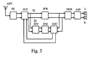
- Figure 3 shows an embodiment of a receiver comprising a mirror suppression circuit according to the invention and providing quadrature signal processing comprising an RF front end FE coupled to antenna means ANT such as known from the cited published patent application WO 01/58029 and comprising (not shown) an RF input stage coupled to the antenna means ANT and followed by a mixer stage for a conversion of an RF signal into an IF signal using a tuning oscillator having a tuning frequency f TO .
- the RF front end FE provides a quadrature IF signal having a frequency disposition as depicted in the diagram of Figure 1B .
- This IF quadrature signal is being supplied to first quadrature signal path S1, which includes error correction circuit ECC followed by a quadrature IF filter stage IFW functioning as first filter circuit and having a resonance frequency at the carrier frequency of said quadrature IF signal, i.e. f IF .
- the selected quadrature IF signal is being supplied to a demodulation circuit DEM to demodulate the same into the baseband modulation signal, e.g. an stereophonic audio signal, which is further processed in an audio signal processor ASP and reproduced with stereo left and right loudspeakers L and R.
- the demodulation circuit DEM may be an FM, PM or AM demodulator, dependent on the RF signal modulation type.
- the first quadrature signal path S1 is being coupled on the one hand from the quadrature output of the IF filter stage IFW to a first quadrature input Idi1, Idq1 of an error detection circuit EDC.
- the first quadrature signal path S1 is coupled prior to said quadrature IF filter stage IFW through second quadrature signal path S2 to second quadrature input Idi2, Idq2 of said error detection circuit EDC.
- the second quadrature signal path S2 includes a cascade connection of an inverter INV and a filter circuit IFM, which preferably is identical to the IF filter stage IFW, said cascade connection being coupled between the quadrature output of the error correction circuit ECC and the second quadrature input Idi2, Idq2 of said error detection circuit EDC.
- the inverter INV and the filter circuit IFM operate together as second filter circuit having a resonance frequency at the negative IF frequency, therewith selecting mirror signals such as mirror signal M in Figure 1B .
- both amplitude and phase errors of the quadrature signal at the output of the error detection circuit EDC and IF signal amplitude variations due to variations in RF fieldstrength, are negatively fed back to the error correction circuit ECC and therewith suppressed.
- the invention is not limited to the embodiments explicitly disclosed. It may well be possible without leaving the scope of the invention, as defined in the claims to dispense with the differential stages 1 and 6 e.g. by correcting for both phase and amplitude mismatch in either the in-phase path I only, or in the phase quadrature path Q only, or to carry out such corrective measure on in-phase and phase quadrature IF oscillator signals VCOI and VCOQ of the local IF tuning oscillator included in the RF front end FE and preceding the first quadrature signal path S1.
- the second filter circuit in the receiver of Figure 3 may well be omitted or may be implemented with a selectivity deviating from the IF filter stage IFW.
Landscapes
- Engineering & Computer Science (AREA)
- Power Engineering (AREA)
- Superheterodyne Receivers (AREA)
- Digital Transmission Methods That Use Modulated Carrier Waves (AREA)
- Bidet-Like Cleaning Device And Other Flush Toilet Accessories (AREA)
- Amplifiers (AREA)
- Circuits Of Receivers In General (AREA)
- Electronic Switches (AREA)
Claims (14)
- Spiegelunterdrückungsschaltung, welche einen ersten Quadratursignalpfad (S1) enthält, der zwischen Anschlüssen eines Quadratursignaleingangs und -ausgangs (Ii, Iq bzw. Oi, Oq) angeschlossen ist und der eine Fehlerkorrekturschaltung (ECC) zur Korrektur von Amplituden- und Phasenfehlern in einem trägermodulierten Quadratursignal einschließt, welches ein Paar Inphasen- und Phasenquadratursignalkomponenten enthält, gekennzeichnet durch einen Quadraturausgang (Oci, Ocq) besagter Fehlerkorrekturschaltung (ECC), der über eine erste Filterschaltung (PFI, IFW) zwecks Selektion besagten Quadratursignals an einen ersten Quadratureingang (Idi1, Idq1) einer Fehlererfassungsschaltung (EDC) angeschlossen ist, wobei besagter erster Quadratursignalpfad (S1) vor besagter erster Filterschaltung (PF1) über einen zweiten Quadratursignalpfad (S2) an einen zweiten Quadratureingang (Idi2, Idq2) besagter Fehlererfassungsschaltung (EDC) angeschlossen ist, wobei besagte Fehlererfassungsschaltung (EDC) Amplituden- und Phasenfehler erfasst und Amplituden- und Phasensteuerungssignale (Ac bzw. Pc) an die Amplituden- und Phasensteuerungseingänge (A bzw. P) besagter Fehlerkorrekturschaltung (ECC) im Hinblick auf eine negative Rückkopplung besagter Amplituden- und Phasenfehler an besagte Fehlerkorrekturschaltung (ECC) liefert, wobei besagtes Amplitudensteuerungssignal (Ac) bei mindestens einem der Produkte Iw *Iref und Qw*Qref variiert und besagtes Phasensteuerungssignal (Pc) bei mindestens einem der Produkte Iw *Qref und Qw*Iref, Iw und Qw bzw. Iref, und Qw variiert, und die Inphasen- und Phasenquadratursignalkomponenten besagten Quadratursignals am ersten Quadratureingang (Idi1, Idq1) der Fehlererfassungsschaltung (EDC) darstellt, beziehungsweise die Inphasen- und Phasenquadratursignalkomponenten eines Quadraturreferenzsignals, das an der negativen Trägerfrequenz besagten Quadratursignals am zweiten Quadratureingang (Idi2, Idq2) der Fehlererfassungsschaltung (EDC) auftritt.
- Spiegelunterdrückungsschaltung gemäß Patentanspruch 1, gekennzeichnet durch besagtes Amplitudensteuerungssignal (Ac), das bei Iw*Iref + Qw*Qref variiert, und besagtes Phasensteuerungssignal (Pc), das bei Iw*Qref - Qw*Iref variiert.
- Spiegelunterdrückungsschaltung gemäß Patentanspruch 1 oder 2, gekennzeichnet durch den zweiten Quadratursignalpfad (S2) einschließlich einer Umkehrvorrichtung (INV), die eine Signalumkehrung beim Erhalt besagten Quadraturreferenzsignals liefert.
- Spiegelunterdrückungsschaltung gemäß einem der Patentansprüche 1 bis 3, dadurch gekennzeichnet, dass besagter zweiter Quadratursignalpfad (S2) nach der Fehlerkorrekturschaltung (ECC) an den ersten Quadratursignalpfad (S1) angeschlossen ist.
- Spiegelunterdrückungsschaltung gemäß einem der Patentansprüche 1 bis 4, gekennzeichnet durch besagten zweiten Quadratursignalpfad (S2) einschließlich einer zweiten Filterschaltung (IFM) zur Selektion besagten Quadraturreferenzsignals.
- Spiegelunterdrückungsschaltung gemäß einem der Patentansprüche 3 bis 5, gekennzeichnet durch besagten zweiten Quadratursignalpfad (S2), welcher besagte Signalumkehrung (INV) enthält, welche zwischen dem ersten Quadratursignalpfad (S 1) und besagter zweiter Filterschaltung (IFM) angeschlossen ist, wobei besagte zweite Filterschaltung (IFM) mit besagter erster Filterschaltung (IFW) identisch ist.
- Empfänger, der eine Quadratursignalverarbeitung liefert, welche eine Hochfrequenz-Eingangsstufe enthält, welcher eine Mischstufe zur Umwandlung eines Hochfrequenzsignals in ein Zwischenfrequenzsignal und eine Zwischenfrequenzstufe zur selektiven Verstärkung besagten Zwischenfrequenzsignals folgt, gekennzeichnet durch eine Spiegelunterdrückungsschaltung gemäß einem der Patentansprüche 1 bis 5, dessen Quadratursignaleingang (Ii, Iq) an einen Quadraturausgang der Mischstufe angeschlossen ist und wobei besagte erste Filterschaltung (IFW) Teil besagter Zwischenfrequenzstufe ist und dessen Eigenfrequenz gleich der Trägerfrequenz besagten Zwischenfrequenzsignals ist.
- Empfänger gemäß Patentanspruch 7, welcher eine Spiegelunterdrückungsschaltung gemäß Patentanspruch 5 enthält, dadurch gekennzeichnet, dass die zweite Filterschaltung (IFM), welche besagtes Quadraturreferenzsignal selektiert, das an der negativen Trägerfrequenz besagten Quadraturzwischenfrequenzsignals auftritt.
- Empfänger gemäß Patentanspruch 8, welcher eine Spiegelunterdrückungsschaltung gemäß Patentanspruch 3 enthält, gekennzeichnet durch besagten zweiten Quadratursignalpfad (S2), welcher besagte Signalumkehrung (INV) enthält, welche zwischen dem ersten Quadratursignalpfad (S 1) und besagter zweiter Filterschaltung (IFM) angeschlossen ist, wobei die zweite Filterschaltung (IFM) mit besagter Zwischenfilterschaltung (IFW) identisch ist.
- Empfänger gemäß Patentanspruch 9, gekennzeichnet durch sowohl eine erste als auch eine zweite Filterschaltung (IFW beziehungsweise IFM), welche Mehrhasenfilter des Resonanzverstärkertyps enthält.
- Empfänger gemäß einem der Patentansprüche 1 bis 10, dadurch gekennzeichnet, dass besagte Fehlerkorrekturschaltung (ECC) eine Amplitudenkorrekturschaltung enthält, welche einen ersten Multiplikator (7) enthält, der in mindestens einem der Paare der Inphasen- und Quadraturpfade des ersten Quadratursignalpfads (S 1) hinsichtlich einer Amplitudenvariation des Signals an besagtem Eingang mit besagtem Amplitudenfehler enthält.
- Empfänger gemäß Patentanspruch 11, gekennzeichnet durch besagte Amplitudenkorrekturschaltung, welche eine Differenzialstufe (6) enthält, welche besagter Erfassungsschaltung (MII, MQQ, A, LPA) folgt, welche besagtes Amplitudensteuerungssignal Ac in ein Differenzialpaar aus erstem und zweiten Amplitudenkontrollsignal umwandelt und dieses an besagten ersten beziehungsweise zweiten Multiplikator (7, 8) liefert, wobei besagter erster und zweiter Multiplikator (7, 8) in besagtem Inphasen- und Quadraturpfad des ersten Quadratursignalpfads (S1) enthalten sind.
- Empfänger gemäß einem der Patentansprüche 1 bis 10, dadurch gekennzeichnet, dass besagte Fehlerkorrekturschaltung (ECC) eine Phasenkorrekturschaltung einschließt, welche einen dritten Multiplikator (2) enthält, dessen Signalausgang an einen der besagten Inphasen- und Quadraturpfade des ersten Quadratursignalpfads (S 1) angeschlossen ist und dessen Signalausgang an ein erstes Additionsgerät (4) angeschlossen ist, welches in dem anderen der besagten Inphasen- und Quadraturpfade eingeschlossen ist, um dorthin einen Teil des Signals zu liefern, welches an besagtem einen Pfad zu besagtem anderen Pfad anliegt, der bei besagtem Phasensteuerungssignal variiert.
- Empfänger gemäß Patentanspruch 13, gekennzeichnet durch besagte Phasenkorrekturschaltung, welche eine Differenzialstufe (1) enthält, welche besagter Erfassungsschaltung (MIQ, MQI, DIF, LPP) folgt, welche besagten Phasenfehler in ein Differenzialpaar aus erstem und zweiten Phasenfehlersignal umwandelt und dieses an Modulationssignaleingänge besagten dritten beziehungsweise vierten Multiplikator (2, 3) liefert, wobei besagter dritter und vierter Multiplikator (2, 3) Eingänge haben, welche an den Phasenquadratur- und Inphasenpfad des ersten Quadratursignalpfads (S 1) angeschlossen sind und dessen Ausgänge an besagtes erstes und ein zweites Additionsgerät (4, 5) angeschlossen sind, welche in besagtem Inphasen- beziehungsweise Phasenquadraturpfad eingeschlossen sind.
Priority Applications (1)
| Application Number | Priority Date | Filing Date | Title |
|---|---|---|---|
| EP03735371A EP1504524B1 (de) | 2002-05-07 | 2003-05-01 | Spiegelunterdrückungsschaltung in einem quadratur-demodulator |
Applications Claiming Priority (4)
| Application Number | Priority Date | Filing Date | Title |
|---|---|---|---|
| EP02076835 | 2002-05-07 | ||
| EP02076835A EP1361655A1 (de) | 2002-05-07 | 2002-05-07 | Spiegelunterdrückungsschaltung in einem quadratur-demodulator |
| PCT/EP2003/004848 WO2003096524A2 (en) | 2002-05-07 | 2003-05-01 | Mirror suppression circuit in a quadrature demodulator |
| EP03735371A EP1504524B1 (de) | 2002-05-07 | 2003-05-01 | Spiegelunterdrückungsschaltung in einem quadratur-demodulator |
Publications (2)
| Publication Number | Publication Date |
|---|---|
| EP1504524A2 EP1504524A2 (de) | 2005-02-09 |
| EP1504524B1 true EP1504524B1 (de) | 2010-04-21 |
Family
ID=29225707
Family Applications (2)
| Application Number | Title | Priority Date | Filing Date |
|---|---|---|---|
| EP02076835A Withdrawn EP1361655A1 (de) | 2002-05-07 | 2002-05-07 | Spiegelunterdrückungsschaltung in einem quadratur-demodulator |
| EP03735371A Expired - Lifetime EP1504524B1 (de) | 2002-05-07 | 2003-05-01 | Spiegelunterdrückungsschaltung in einem quadratur-demodulator |
Family Applications Before (1)
| Application Number | Title | Priority Date | Filing Date |
|---|---|---|---|
| EP02076835A Withdrawn EP1361655A1 (de) | 2002-05-07 | 2002-05-07 | Spiegelunterdrückungsschaltung in einem quadratur-demodulator |
Country Status (7)
| Country | Link |
|---|---|
| US (1) | US7242730B2 (de) |
| EP (2) | EP1361655A1 (de) |
| JP (1) | JP4429161B2 (de) |
| AT (1) | ATE465547T1 (de) |
| AU (1) | AU2003236635A1 (de) |
| DE (1) | DE60332225D1 (de) |
| WO (1) | WO2003096524A2 (de) |
Families Citing this family (14)
| Publication number | Priority date | Publication date | Assignee | Title |
|---|---|---|---|---|
| JP3902184B2 (ja) * | 2004-02-24 | 2007-04-04 | 株式会社アドバンテスト | 直交変調装置、方法、プログラム、記録媒体 |
| JP4376689B2 (ja) * | 2004-04-21 | 2009-12-02 | 富士通株式会社 | 直交変調システム |
| US7382834B2 (en) | 2004-05-06 | 2008-06-03 | Beceem Communications Inc. | Phase rotation estimation |
| US7822399B2 (en) | 2007-05-11 | 2010-10-26 | Telefonaktiebolaget Lm Ericsson (Publ) | Image compensation for wireless receiver |
| US7894555B2 (en) * | 2007-08-02 | 2011-02-22 | Telefonaktiebolaget Lm Ericsson (Publ) | IQ imbalance image suppression |
| US7986930B2 (en) * | 2007-08-02 | 2011-07-26 | Telefonaktiebolaget Lm Ericsson (Publ) | IQ imbalance image suppression in presence of unknown phase shift |
| JP5620395B2 (ja) * | 2008-12-01 | 2014-11-05 | ノーテル・ネットワークス・リミテッド | デジタル・フィルタおよび帯域阻止フィルタリングを使用する周波数可変フィルタ |
| RU2569578C1 (ru) * | 2014-08-01 | 2015-11-27 | Федеральное государственное бюджетное образовательное учреждение высшего профессионального образования "Московский государственнный университет путей сообзщения" МГУПС (МИИТ) | Фазокомпенсационный подавитель зеркального канала в приемнике радиосигналов |
| CN106817136B (zh) * | 2017-02-21 | 2022-09-16 | 和芯星通科技(北京)有限公司 | 一种实现正交信号处理的方法、装置及接收机 |
| US10241844B2 (en) * | 2017-05-11 | 2019-03-26 | Intel Corporation | Techniques for heat spreading in an integrated circuit |
| CN110689874A (zh) * | 2019-09-06 | 2020-01-14 | Oppo广东移动通信有限公司 | 一种载波电路和定向发声设备 |
| CN114944845B (zh) * | 2022-06-16 | 2023-03-10 | 北京大有半导体有限责任公司 | 镜像干扰抑制方法、装置及电子设备、低/零中频接收机 |
| CN115483958B (zh) * | 2022-08-17 | 2023-07-28 | 西安空间无线电技术研究所 | 微波测距信号的低噪声接收高精度相位测量系统及方法 |
| US12463592B2 (en) | 2023-06-23 | 2025-11-04 | Qualcomm Incorporated | Active mixers with enhanced image rejection ratio (IRR) |
Family Cites Families (28)
| Publication number | Priority date | Publication date | Assignee | Title |
|---|---|---|---|---|
| JPS6150354U (de) * | 1984-09-03 | 1986-04-04 | ||
| DE3889326D1 (de) * | 1988-05-27 | 1994-06-01 | Itt Ind Gmbh Deutsche | Korrekturschaltung für ein digitales Quadratur-Signalpaar. |
| US5034965A (en) * | 1988-11-11 | 1991-07-23 | Matsushita Electric Industrial Co., Ltd. | Efficient coding method and its decoding method |
| KR0151379B1 (ko) * | 1989-04-21 | 1999-09-01 | 프레데릭 얀 스미스 | 동조 가능한 공진 증폭기, 주파수 합성회로 및 슈퍼헤테로다인 fm 수신기 |
| GB2238197A (en) * | 1989-11-16 | 1991-05-22 | Motorola Inc | Feed-forward amplifier with amplitude and phase pre-correction |
| SE470455B (sv) * | 1992-08-24 | 1994-04-11 | Ericsson Telefon Ab L M | Anordning för kompensering av fasvridningen i återkopplingsslingan vid en kartesiskt återkopplad effektförstärkare |
| US5551070A (en) * | 1993-01-28 | 1996-08-27 | Telefonaktiebolaget Lm Ericsson | Cartesian multicarrier feedback |
| US6408008B1 (en) * | 1993-04-06 | 2002-06-18 | Creative Integrated Systems, Inc. | Circuit for attenuation of echos caused by line variations and an interfacing system for capacitively coupling a plurality of sources to a two-wire communication line |
| US5461426A (en) * | 1993-08-20 | 1995-10-24 | Samsung Electronics Co., Ltd. | Apparatus for processing modified NTSC television signals, with digital signals buried therewithin |
| US5826180A (en) * | 1994-08-08 | 1998-10-20 | Nice Systems Ltd. | Near homodyne radio frequency receiver |
| JPH10327204A (ja) * | 1997-05-26 | 1998-12-08 | Nec Corp | 等化器を用いた位相同期ループ回路 |
| SE512623C2 (sv) * | 1997-11-03 | 2000-04-10 | Ericsson Telefon Ab L M | Förfarande och anordning i ett telekommunikationsproblem |
| US6130918A (en) * | 1997-12-01 | 2000-10-10 | Nortel Networks Limited | Method and apparatus for reducing the peak-to-average ratio in a multicarrier communication system |
| US7593481B2 (en) * | 1998-08-31 | 2009-09-22 | Kamilo Feher | CDMA, W-CDMA, 3rd generation interoperable modem format selectable (MFS) systems with GMSK modulated systems |
| GB9817675D0 (en) * | 1998-08-13 | 1998-10-07 | Simoco Int Ltd | Error correction in amplifiers |
| GB2345230B (en) * | 1998-12-23 | 2003-10-29 | Nokia Mobile Phones Ltd | Radio receiver and a filter for the radio receiver |
| US6470060B1 (en) * | 1999-03-01 | 2002-10-22 | Micron Technology, Inc. | Method and apparatus for generating a phase dependent control signal |
| US6714776B1 (en) * | 1999-09-28 | 2004-03-30 | Microtune (Texas), L.P. | System and method for an image rejecting single conversion tuner with phase error correction |
| JP2003522456A (ja) * | 2000-02-04 | 2003-07-22 | コーニンクレッカ フィリップス エレクトロニクス エヌ ヴィ | 無線fm受信器 |
| US6778594B1 (en) * | 2000-06-12 | 2004-08-17 | Broadcom Corporation | Receiver architecture employing low intermediate frequency and complex filtering |
| US6671340B1 (en) * | 2000-06-15 | 2003-12-30 | Ibiquity Digital Corporation | Method and apparatus for reduction of interference in FM in-band on-channel digital audio broadcasting receivers |
| EP1168597A1 (de) * | 2000-06-23 | 2002-01-02 | NTT DoCoMo, Inc. | Quadraturempfänger mit Orthogonalitätskorrektur |
| US20020146996A1 (en) * | 2001-03-06 | 2002-10-10 | Bachman Thomas A. | Scanning receiver for use in power amplifier linearization |
| US6819911B2 (en) * | 2001-04-02 | 2004-11-16 | General Dynamics Decision Systems, Inc. | Active interference suppressor utilizing recombinant transmultiplexing |
| US6785341B2 (en) * | 2001-05-11 | 2004-08-31 | Qualcomm Incorporated | Method and apparatus for processing data in a multiple-input multiple-output (MIMO) communication system utilizing channel state information |
| US6735264B2 (en) * | 2001-08-31 | 2004-05-11 | Rainmaker Technologies, Inc. | Compensation for non-linear distortion in a modem receiver |
| EP1300956A1 (de) * | 2001-10-02 | 2003-04-09 | Matsushita Electric Industrial Co., Ltd. | Empfangsvorrichtung |
| US6563885B1 (en) * | 2001-10-24 | 2003-05-13 | Texas Instruments Incorporated | Decimated noise estimation and/or beamforming for wireless communications |
-
2002
- 2002-05-07 EP EP02076835A patent/EP1361655A1/de not_active Withdrawn
-
2003
- 2003-05-01 AU AU2003236635A patent/AU2003236635A1/en not_active Abandoned
- 2003-05-01 JP JP2004504375A patent/JP4429161B2/ja not_active Expired - Fee Related
- 2003-05-01 AT AT03735371T patent/ATE465547T1/de not_active IP Right Cessation
- 2003-05-01 DE DE60332225T patent/DE60332225D1/de not_active Expired - Lifetime
- 2003-05-01 US US10/509,210 patent/US7242730B2/en not_active Expired - Fee Related
- 2003-05-01 EP EP03735371A patent/EP1504524B1/de not_active Expired - Lifetime
- 2003-05-01 WO PCT/EP2003/004848 patent/WO2003096524A2/en not_active Ceased
Also Published As
| Publication number | Publication date |
|---|---|
| US7242730B2 (en) | 2007-07-10 |
| DE60332225D1 (de) | 2010-06-02 |
| ATE465547T1 (de) | 2010-05-15 |
| WO2003096524A3 (en) | 2004-05-13 |
| EP1504524A2 (de) | 2005-02-09 |
| WO2003096524A2 (en) | 2003-11-20 |
| JP4429161B2 (ja) | 2010-03-10 |
| EP1361655A1 (de) | 2003-11-12 |
| AU2003236635A1 (en) | 2003-11-11 |
| US20050226352A1 (en) | 2005-10-13 |
| AU2003236635A8 (en) | 2003-11-11 |
| HK1075752A1 (en) | 2005-12-23 |
| JP2005525037A (ja) | 2005-08-18 |
Similar Documents
| Publication | Publication Date | Title |
|---|---|---|
| EP1504524B1 (de) | Spiegelunterdrückungsschaltung in einem quadratur-demodulator | |
| US7120414B2 (en) | Circuit and method for receiving and mixing radio frequencies in a direct conversion receiver | |
| US5613233A (en) | Apparatus with distortion cancelling feedback signal | |
| US7457606B2 (en) | Mixer circuit for direct conversion transceiver with improved IP2 | |
| US6999746B2 (en) | Image rejection mixer | |
| JP3928898B2 (ja) | 集積イメージ阻止ミキサ | |
| JP3398910B2 (ja) | イメージ除去型受信機 | |
| EP1478097B1 (de) | Direktkonversionsempfänger mit Gleichspannungsoffset-Reduzierung und Sender | |
| JPH0691477B2 (ja) | Rf同調回路 | |
| US20090131006A1 (en) | Apparatus, integrated circuit, and method of compensating iq phase mismatch | |
| GB2296835A (en) | Active filter arrangement | |
| US7536165B2 (en) | Offset correction for down-conversion mixers | |
| US6628343B1 (en) | Television signal reception circuit, automatic phase shift control circuit and equal amplitude addition circuit | |
| EP1199796B1 (de) | Frequenzumsetzer | |
| US20070190959A1 (en) | Apparatus and method for frequency conversion with minimized intermodulation distortion | |
| JP4705041B2 (ja) | フィードバックを有するミキサ | |
| US7227912B2 (en) | Receiver with mirror frequency suppression | |
| EP1652292B1 (de) | Offsetkorrektur für abwärtsumsetzungsmischer | |
| HK1075752B (en) | Mirror suppression circuit in a quadrature demodulator | |
| US4616186A (en) | FM quadrature demodulator with distortion compensation | |
| JP3993555B2 (ja) | 周波数変換機能を有する電子回路装置及びこれを用いた無線通信装置 | |
| US20200382059A1 (en) | Image rejection mixer and communication circuit | |
| JPH1141063A (ja) | 自動移相制御回路 |
Legal Events
| Date | Code | Title | Description |
|---|---|---|---|
| PUAI | Public reference made under article 153(3) epc to a published international application that has entered the european phase |
Free format text: ORIGINAL CODE: 0009012 |
|
| 17P | Request for examination filed |
Effective date: 20041116 |
|
| AK | Designated contracting states |
Kind code of ref document: A2 Designated state(s): AT BE BG CH CY CZ DE DK EE ES FI FR GB GR HU IE IT LI LU MC NL PT RO SE SI SK TR |
|
| AX | Request for extension of the european patent |
Extension state: AL LT LV MK |
|
| DAX | Request for extension of the european patent (deleted) | ||
| REG | Reference to a national code |
Ref country code: HK Ref legal event code: DE Ref document number: 1075752 Country of ref document: HK |
|
| 17Q | First examination report despatched |
Effective date: 20070522 |
|
| GRAP | Despatch of communication of intention to grant a patent |
Free format text: ORIGINAL CODE: EPIDOSNIGR1 |
|
| GRAS | Grant fee paid |
Free format text: ORIGINAL CODE: EPIDOSNIGR3 |
|
| GRAA | (expected) grant |
Free format text: ORIGINAL CODE: 0009210 |
|
| RAP1 | Party data changed (applicant data changed or rights of an application transferred) |
Owner name: SEMICONDUCTOR IDEAS TO THE MARKET (ITOM) BV |
|
| AK | Designated contracting states |
Kind code of ref document: B1 Designated state(s): AT BE BG CH CY CZ DE DK EE ES FI FR GB GR HU IE IT LI LU MC NL PT RO SE SI SK TR |
|
| REG | Reference to a national code |
Ref country code: GB Ref legal event code: FG4D |
|
| REG | Reference to a national code |
Ref country code: CH Ref legal event code: EP |
|
| REG | Reference to a national code |
Ref country code: IE Ref legal event code: FG4D |
|
| REF | Corresponds to: |
Ref document number: 60332225 Country of ref document: DE Date of ref document: 20100602 Kind code of ref document: P |
|
| REG | Reference to a national code |
Ref country code: NL Ref legal event code: VDEP Effective date: 20100421 |
|
| PG25 | Lapsed in a contracting state [announced via postgrant information from national office to epo] |
Ref country code: NL Free format text: LAPSE BECAUSE OF FAILURE TO SUBMIT A TRANSLATION OF THE DESCRIPTION OR TO PAY THE FEE WITHIN THE PRESCRIBED TIME-LIMIT Effective date: 20100421 Ref country code: SE Free format text: LAPSE BECAUSE OF FAILURE TO SUBMIT A TRANSLATION OF THE DESCRIPTION OR TO PAY THE FEE WITHIN THE PRESCRIBED TIME-LIMIT Effective date: 20100421 Ref country code: ES Free format text: LAPSE BECAUSE OF FAILURE TO SUBMIT A TRANSLATION OF THE DESCRIPTION OR TO PAY THE FEE WITHIN THE PRESCRIBED TIME-LIMIT Effective date: 20100801 |
|
| PG25 | Lapsed in a contracting state [announced via postgrant information from national office to epo] |
Ref country code: FI Free format text: LAPSE BECAUSE OF FAILURE TO SUBMIT A TRANSLATION OF THE DESCRIPTION OR TO PAY THE FEE WITHIN THE PRESCRIBED TIME-LIMIT Effective date: 20100421 Ref country code: AT Free format text: LAPSE BECAUSE OF FAILURE TO SUBMIT A TRANSLATION OF THE DESCRIPTION OR TO PAY THE FEE WITHIN THE PRESCRIBED TIME-LIMIT Effective date: 20100421 Ref country code: SI Free format text: LAPSE BECAUSE OF FAILURE TO SUBMIT A TRANSLATION OF THE DESCRIPTION OR TO PAY THE FEE WITHIN THE PRESCRIBED TIME-LIMIT Effective date: 20100421 |
|
| PG25 | Lapsed in a contracting state [announced via postgrant information from national office to epo] |
Ref country code: GR Free format text: LAPSE BECAUSE OF FAILURE TO SUBMIT A TRANSLATION OF THE DESCRIPTION OR TO PAY THE FEE WITHIN THE PRESCRIBED TIME-LIMIT Effective date: 20100722 Ref country code: CY Free format text: LAPSE BECAUSE OF FAILURE TO SUBMIT A TRANSLATION OF THE DESCRIPTION OR TO PAY THE FEE WITHIN THE PRESCRIBED TIME-LIMIT Effective date: 20100421 Ref country code: MC Free format text: LAPSE BECAUSE OF NON-PAYMENT OF DUE FEES Effective date: 20100531 |
|
| REG | Reference to a national code |
Ref country code: CH Ref legal event code: PL |
|
| REG | Reference to a national code |
Ref country code: HK Ref legal event code: GR Ref document number: 1075752 Country of ref document: HK |
|
| PG25 | Lapsed in a contracting state [announced via postgrant information from national office to epo] |
Ref country code: DK Free format text: LAPSE BECAUSE OF FAILURE TO SUBMIT A TRANSLATION OF THE DESCRIPTION OR TO PAY THE FEE WITHIN THE PRESCRIBED TIME-LIMIT Effective date: 20100421 Ref country code: PT Free format text: LAPSE BECAUSE OF FAILURE TO SUBMIT A TRANSLATION OF THE DESCRIPTION OR TO PAY THE FEE WITHIN THE PRESCRIBED TIME-LIMIT Effective date: 20100823 Ref country code: EE Free format text: LAPSE BECAUSE OF FAILURE TO SUBMIT A TRANSLATION OF THE DESCRIPTION OR TO PAY THE FEE WITHIN THE PRESCRIBED TIME-LIMIT Effective date: 20100421 |
|
| PLBE | No opposition filed within time limit |
Free format text: ORIGINAL CODE: 0009261 |
|
| STAA | Information on the status of an ep patent application or granted ep patent |
Free format text: STATUS: NO OPPOSITION FILED WITHIN TIME LIMIT |
|
| PG25 | Lapsed in a contracting state [announced via postgrant information from national office to epo] |
Ref country code: BE Free format text: LAPSE BECAUSE OF FAILURE TO SUBMIT A TRANSLATION OF THE DESCRIPTION OR TO PAY THE FEE WITHIN THE PRESCRIBED TIME-LIMIT Effective date: 20100421 Ref country code: CH Free format text: LAPSE BECAUSE OF NON-PAYMENT OF DUE FEES Effective date: 20100531 Ref country code: CZ Free format text: LAPSE BECAUSE OF FAILURE TO SUBMIT A TRANSLATION OF THE DESCRIPTION OR TO PAY THE FEE WITHIN THE PRESCRIBED TIME-LIMIT Effective date: 20100421 Ref country code: LI Free format text: LAPSE BECAUSE OF NON-PAYMENT OF DUE FEES Effective date: 20100531 Ref country code: RO Free format text: LAPSE BECAUSE OF FAILURE TO SUBMIT A TRANSLATION OF THE DESCRIPTION OR TO PAY THE FEE WITHIN THE PRESCRIBED TIME-LIMIT Effective date: 20100421 Ref country code: SK Free format text: LAPSE BECAUSE OF FAILURE TO SUBMIT A TRANSLATION OF THE DESCRIPTION OR TO PAY THE FEE WITHIN THE PRESCRIBED TIME-LIMIT Effective date: 20100421 |
|
| 26N | No opposition filed |
Effective date: 20110124 |
|
| PG25 | Lapsed in a contracting state [announced via postgrant information from national office to epo] |
Ref country code: IT Free format text: LAPSE BECAUSE OF FAILURE TO SUBMIT A TRANSLATION OF THE DESCRIPTION OR TO PAY THE FEE WITHIN THE PRESCRIBED TIME-LIMIT Effective date: 20100421 |
|
| PG25 | Lapsed in a contracting state [announced via postgrant information from national office to epo] |
Ref country code: IE Free format text: LAPSE BECAUSE OF NON-PAYMENT OF DUE FEES Effective date: 20100501 |
|
| PG25 | Lapsed in a contracting state [announced via postgrant information from national office to epo] |
Ref country code: LU Free format text: LAPSE BECAUSE OF NON-PAYMENT OF DUE FEES Effective date: 20100501 Ref country code: HU Free format text: LAPSE BECAUSE OF FAILURE TO SUBMIT A TRANSLATION OF THE DESCRIPTION OR TO PAY THE FEE WITHIN THE PRESCRIBED TIME-LIMIT Effective date: 20101022 Ref country code: BG Free format text: LAPSE BECAUSE OF FAILURE TO SUBMIT A TRANSLATION OF THE DESCRIPTION OR TO PAY THE FEE WITHIN THE PRESCRIBED TIME-LIMIT Effective date: 20100421 |
|
| PG25 | Lapsed in a contracting state [announced via postgrant information from national office to epo] |
Ref country code: TR Free format text: LAPSE BECAUSE OF FAILURE TO SUBMIT A TRANSLATION OF THE DESCRIPTION OR TO PAY THE FEE WITHIN THE PRESCRIBED TIME-LIMIT Effective date: 20100421 |
|
| PG25 | Lapsed in a contracting state [announced via postgrant information from national office to epo] |
Ref country code: BG Free format text: LAPSE BECAUSE OF FAILURE TO SUBMIT A TRANSLATION OF THE DESCRIPTION OR TO PAY THE FEE WITHIN THE PRESCRIBED TIME-LIMIT Effective date: 20100721 |
|
| REG | Reference to a national code |
Ref country code: DE Ref legal event code: R084 Ref document number: 60332225 Country of ref document: DE Effective date: 20140520 |
|
| REG | Reference to a national code |
Ref country code: FR Ref legal event code: PLFP Year of fee payment: 14 |
|
| REG | Reference to a national code |
Ref country code: FR Ref legal event code: PLFP Year of fee payment: 15 |
|
| REG | Reference to a national code |
Ref country code: FR Ref legal event code: PLFP Year of fee payment: 16 |
|
| PGFP | Annual fee paid to national office [announced via postgrant information from national office to epo] |
Ref country code: FR Payment date: 20190524 Year of fee payment: 17 |
|
| GBPC | Gb: european patent ceased through non-payment of renewal fee |
Effective date: 20200501 |
|
| PG25 | Lapsed in a contracting state [announced via postgrant information from national office to epo] |
Ref country code: FR Free format text: LAPSE BECAUSE OF NON-PAYMENT OF DUE FEES Effective date: 20200531 Ref country code: GB Free format text: LAPSE BECAUSE OF NON-PAYMENT OF DUE FEES Effective date: 20200501 |
|
| PGFP | Annual fee paid to national office [announced via postgrant information from national office to epo] |
Ref country code: DE Payment date: 20220527 Year of fee payment: 20 |
|
| REG | Reference to a national code |
Ref country code: DE Ref legal event code: R071 Ref document number: 60332225 Country of ref document: DE |